ASML sets density record with latest chipmaking tools — High-NA EUV equipment prints first patterns
ASML reaches another milestone.

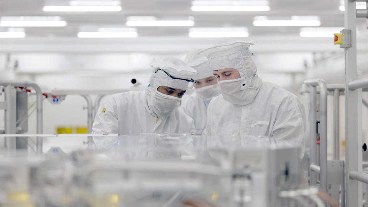
ASML has announced that its first extreme ultraviolet (EUV) lithography tool with projection optics featuring a 0.55 numerical aperture (High-NA) has printed its first patterns. The announcement is a major milestone for both ASML and for High-NA EUV lithography technology in general.
"Our High-NA EUV system in Veldhoven printed the first-ever 10 nanometer dense lines," a statement by ASML reads. "Imaging was done after optics, sensors and stages completed coarse calibration. Next up: bringing the system to full performance. And achieving the same results in the field."
There are currently two High-NA EUV litho systems in the world: one is being built by ASML in Veldhoven, Netherlands — where ASML is headquartered and where the company has a joint High-NA lab with Imec, a leading semiconductor research institute in Belgium; another is being assembled at Intel's D1X fab near Hillsboro, Oregon.
Article continues belowASML seems to be the first company to announce successful patterning using a High-NA EUV lithography system, which is a major milestone for the entire semiconductor industry. ASML will only use its Twinscan EXE:5000 for its own development and for refining its own technology.
By contrast, Intel will use its Twinscan EXE:5000 to learn how to use High-NA EUV lithography for mass producing chips. Intel will adopt this tool for R&D purposes with its Intel 18A (1.8nm-class) process technology, and plans to deploy the next-generation Twinscan EXE:5200 scanners to make chips on its 14A (1.4nm-class) production node.
ASML's Twinscan EXE:5200, which is equipped with a 0.55 NA lens, is designed to print chips with an 8nm resolution — a significant improvement over the current 13nm resolution of EUV tools. This technology allows for printing transistors that are 1.7 times smaller and achieve 2.9 times higher transistor densities with a single exposure, versus Low-NA tools.
Although Low-NA systems can match this resolution, they have to use a costly double-patterning technique. Achieving 8nm is critical for manufacturing sub-3nm process chips, which are set to arrive in 2025–2026. The introduction of High-NA EUV technology is set to eliminate the need for EUV double patterning — thereby streamlining production processes, potentially enhancing yields, and cutting costs. However, High-NA tools cost up to $400 million each and introduce numerous challenges, which have complicated the transition to leading-edge process technologies (set to happen in the second half of the decade).
Get Tom's Hardware's best news and in-depth reviews, straight to your inbox.

Anton Shilov is a contributing writer at Tom’s Hardware. Over the past couple of decades, he has covered everything from CPUs and GPUs to supercomputers and from modern process technologies and latest fab tools to high-tech industry trends.
-
elforeign Will the cost for the High NA tools remain the same over their lifetime or will they come down in price? Can't imagine very many of these going out to customers given the capital required and the inability for the Chinese to buy these.Reply
Aside from Intel, TSMC and R&D at IMEC and ASML, how many others would realistically be looking at using these? Samsung, any of the other DRAM makers or Japanese/European fabs? -
JarredWaltonGPU Reply
Like any technology, early adopters will pay a lot more — to cover the R&D behind the tech, among other things. I don't know how much prices will drop over the lifetime of the Twinscan EX:5000 as an example, but presumably at some point in 5~10 years they'll be more readily available for what will then be trailing edge nodes.elforeign said:Will the cost for the High NA tools remain the same over their lifetime or will they come down in price? Can't imagine very many of these going out to customers given the capital required and the inability for the Chinese to buy these.
Aside from Intel, TSMC and R&D at IMEC and ASML, how many others would realistically be looking at using these? Samsung, any of the other DRAM makers or Japanese/European fabs?