Taiwan's TSMC is exploring the possibility of building an advanced packaging facility in Japan, reports Reuters. The company is about to begin chip production in the island nation, so building an advanced packaging facility is a natural move from TSMC. And if the company proceeds with the plan, it will significantly bolster Japan's semiconductor industry revival efforts.
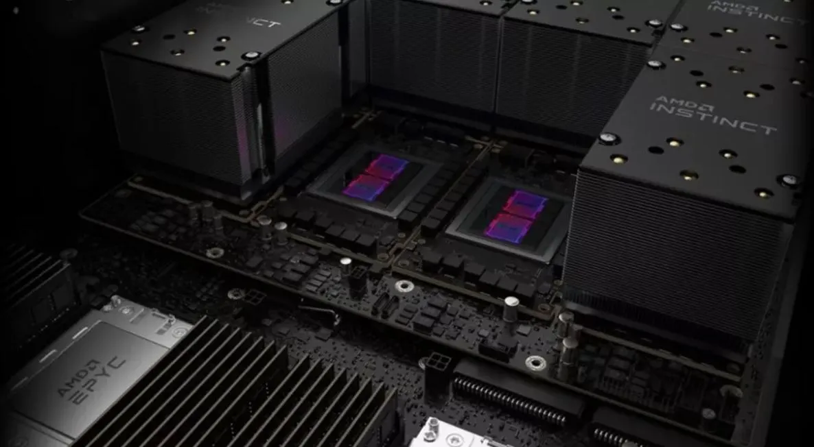
TSMC is considering the introduction of its chip-on-wafer-on-substrate-series (CoWoS) packaging technology to Japan, the report says. This advanced technology is used to build high-performance processors, such as Apple's M2 Ultra for desktop workstations, AMD's Instinct MI-300 processor for AI and HPC, as well as Nvidia's H100 GPU for artificial intelligence and high-performance computing. At present, TSMC's entire CoWoS capacity is based in Taiwan, but it looks like that could change, with additional CoWoS capacity in Japan as well.
The discussions are in their initial stages, with no firm decisions made regarding investment scale or timelines, the report says. TSMC declined to comment to Reuters on its plans for Japan, but building additional CoWoS capacity would be in line with TSMC's general strategy.
Article continues below
TSMC's footprint in Japan is already growing. One fab has been built and equipped and another semiconductor fabrication facility in Kyushu has been announced. The collaboration with Japanese corporations such as Sony and Toyota is a part of TSMC's expansion strategy, and the company's total investments in the Japan venture are expected to exceed $20 billion.
In addition to its potential expansion in Japan, TSMC is also increasing its advanced packaging capacity in Taiwan. The company recently revealed plans for additional capacity in Chiayi, southern Taiwan, to meet the surging market demand. Construction of a new CoWoS plant in Chiayi is set to commence in early May.
The global demand for advanced semiconductor packaging has seen a significant uptick, driven largely by the rapid growth of AI processors, primarily Nvidia's H100. In response, TSMC has announced plans to double its CoWoS output by the end of the year and anticipates further expansion in 2025.
In general, TSMC's potential move to build advanced packaging capacity in Japan, along with its ongoing expansion in Taiwan and collaborations in Japan, highlights the company's proactive approach to meeting increasing global demands for advanced chip production and packaging.

