Inside Western Digital: How Tomorrow's Storage Gets Made
Hold The Onions
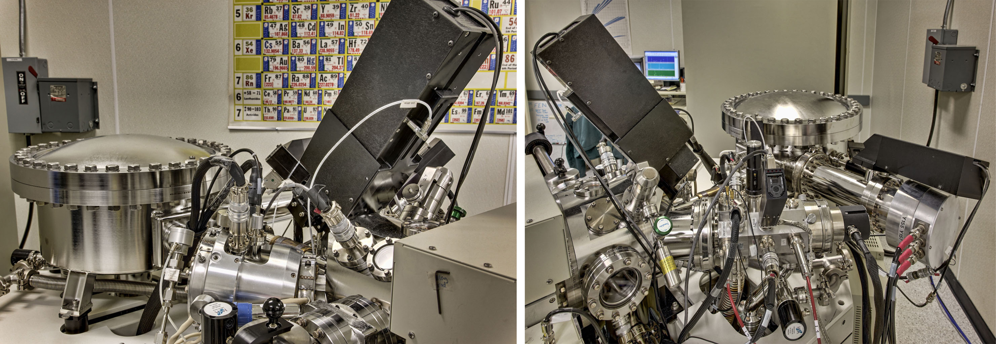
The last time I touched an “auger,” it was a drill used for digging post holes in the ground. This tool is an “Auger nanoprobe.” It’s even more surface sensitive than ESCA, but it can’t dig holes, even tiny ones. The device performs Time-of-Flight Secondary Ion Mass Spectrometry (ToF-SIMS), giving WD the ability to detect single molecular layers on a surface. In ToF-SIMS, “a beam of primary atomic ions is directed onto a surface, which produces an array of secondary ions characteristic of the surface species.” Essentially, this allows for molecule-specific identification of trace contaminants within the disk drive, especially at the vulnerable head/disk interface. As with ESCA and TEM, materials to be identified must be in an ultra-high vacuum environment.
“The Auger takes a primary ion beam from a gold gun source, shoots it at the sample, and looks at the secondary ions coming off of the sample,” explained WD. “You can get a lot of data fairly quickly from an instrument like this. All analytical instruments have good points and bad points, and you try to play them off of each other to get a complete answer. The good point of this is you have a mass spectrum of your samples, and that can be a very precise way to identify contaminants, even in very small amounts, and what their source is. But because it’s so very sensitive, it can have parts per billion level sensitivity for some elements. You’re looking at such a very fine, fine cut of the surface, so interpretation can be difficult. You have to separate what you’re interested in and what’s extraneous contamination. Interpretation is usually one of the more difficult parts of this technique.”
“If you breathed heavy on a sample,” the Auger’s technician added, “I could probably tell.” Given the sandwich I’d had only minutes before, I suspected atomic analysis wouldn’t be necessary for this. Still, it was the closest thing to a joke I would hear from a technical employee for the entire day.
Platter Scrap
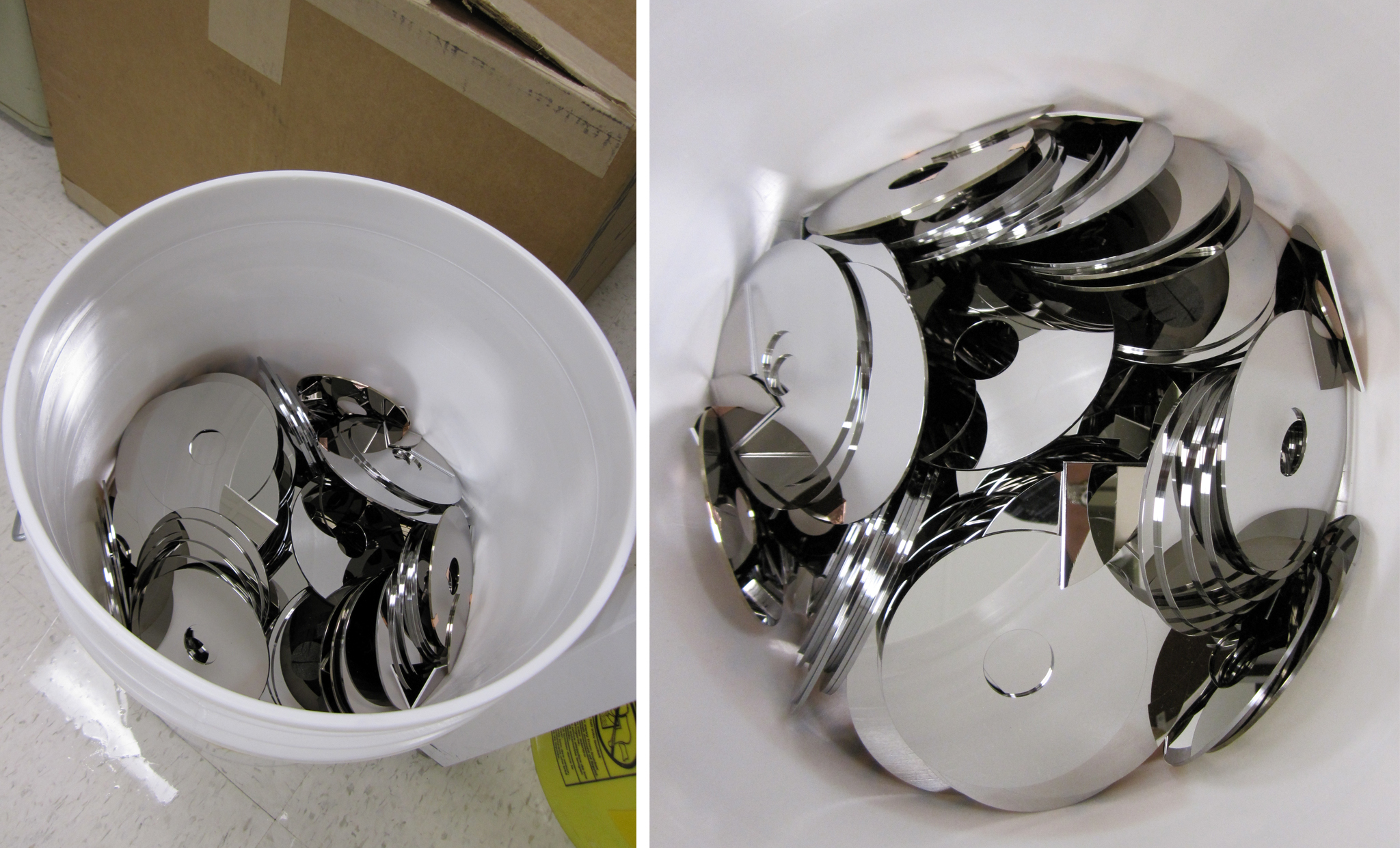
As we left the analysis area and concluded our tour of San Jose 2, I happened to glance down at a white bucket in the hallway. You can see its contents—dozens of broken and discarded media platters. I should have grabbed a few as souvenirs. The bucket spoke to me, saying, “you have to break a few hundred thousand eggs to make a mass storage omelet.” Or something like that. In any case, the clear message that emerged from my Media Operations tour was that there is a vast amount of trial and error, analysis and reanalysis, production and refinement, that goes into every little step in disk design. I’m not exactly sure what I had thought the process entailed before this day. It might only take one engineer to screw in a lightbulb, but apparently it takes hundreds of them spread across an immense acreage of ultra-modern machinery and facilities to keep designing better light bulbs. We go to Best Buy or Newegg and pay our $100 or $200 for another terabyte or so to hold our files, never giving a thought to the immense effort and expense that went into making all of that capacity so affordable.
The scary thing was that I wasn’t even half-way into my tour.
Matters Come To A Head
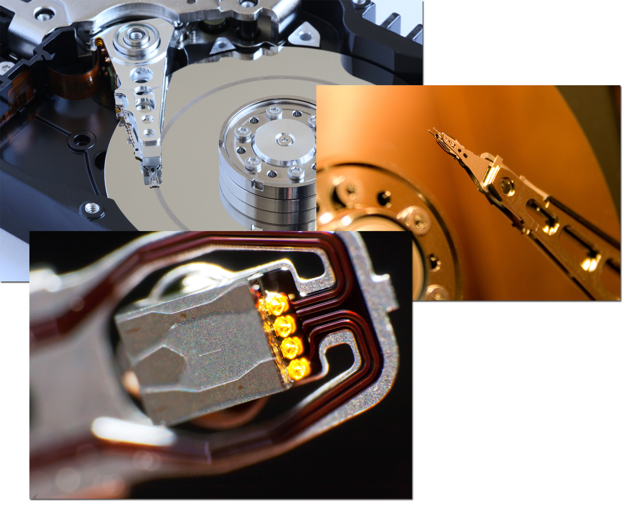
Those of us familiar with LPs might naturally associate the head of a hard drive with the needle of a record player. I suppose I went into the WD Magnetic Head Facility in Fremont expecting something vaguely simple, like a needle, some sort of magnetic device that conducted pulses to and from the media and rest of the drive. I had no idea that the magnetic read/write head is every bit as complex and critical as the media itself. Once again, I drastically underestimated the resources and processes needed to make this tiny, conceptually simple object. Or, as my lead engineer host said when I showed my ignorance that building a read head involved sputtering, “Wow, I guess this is going to require a much more basic explanation than I’d thought.” Nice.
These images, including the great shot of a head crash, were borrowed from Wikimedia Commons. I’ll return them when we’re done.
Get Tom's Hardware's best news and in-depth reviews, straight to your inbox.
Yellow World
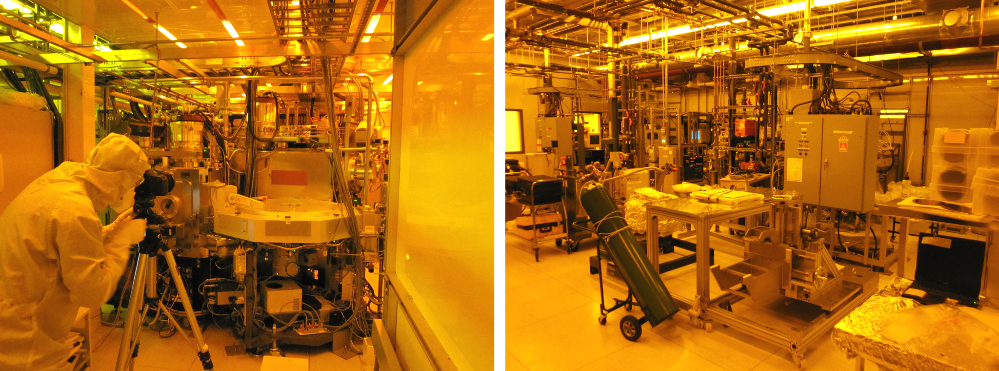
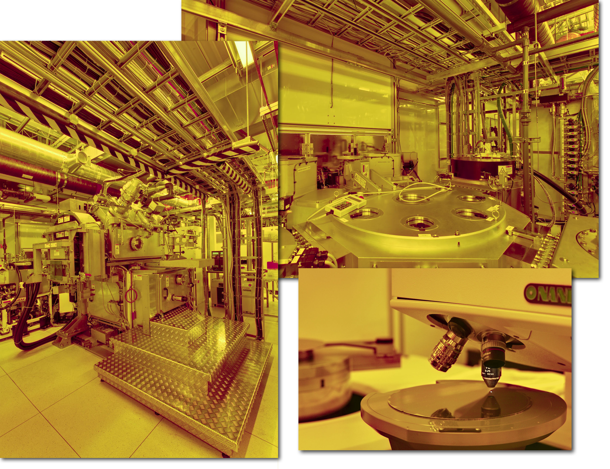
In the following images, you’ll immediately notice that everything is yellow. We could have color corrected this to make the images clearer, but this is how things actually look in a manufacturing area that produces semiconductor wafer-based microsystems. Part of the manufacturing process involves photolithography, which requires the exposure of photoresist to certain light wavelengths. This is much like photography, wherein if you expose undeveloped film to regular white light, it will destroy the film. The wafer’s photoresist doesn’t react to yellow light, so wide swaths of this facility exist in this dimmed, surreal state. Specifically, the fluorescent lighting seen throughout this area is filtered to eliminate blue and ultraviolet wavelengths, instead focusing on light in the roughly 550 to 650nm range.
Tip Of The PVD Iceberg
Here we see the Physical Vapor Deposition (PVD) tool use to deposit the Tunneling Magneto-Resistive (TMR) stack. The TMR stack consists of several layers of complex materials, each of which has a thickness measured in angstroms. The thinnest of them is less than 10 angstroms, so incredible precision and control over the process is essential. According to WD, the TMR stack is the most critical component of the reader portion of the read-write head.
It’s difficult to convey how imposing these machines are. Standing next to it, I’d say the PVD tool has a footprint large enough to fill my living room. However, the loading and unloading interface with the machine is done via the outside hallway through a little door, sort of like the exposed tip of an iceberg. Many of the tools in this building have such loading gateways, designed to minimize and automate human interaction with the machines and thus reduce the chance of variables and accidents in the process. Monitoring and control terminals usually sit alongside the loading gate. On the right, you can see Heather using one of these to check her email (kidding).
Seeding Conductivity
This Physical Vapor Deposition tool is used to deposit very thin layers called seedlayers. Seedlayers are metallic and magnetic “starting” layers deposited on top of non-conductive substrate layers. A seedlayer can provide electrical conductivity to enable the subsequent electroplating process.
My guide informed me that “metrology is widely used and required throughout the head process flow.” This is engineering-speak for “we measure everything to make sure it’s right.” Upon leaving the PVD area, this gizmo caught my eye because it looked like a microscope—something vaguely familiar! It’s not a microscope, of course. It’s a tool for measuring a wafer’s thickness conformance, which is obviously a key concern as you pile layer after layer onto it.
Isn’t There A 5-Second Rule?
In addition to PVD, Western Digital also uses electroplating to process some of the thicker metallic layers in both the read and write head process blocks. What you see here are the front and back sides of a typical electroplating station. Once the technician places the wafer, the tool handles all subsequent handling until its return—again, trying to keep humans out of the process as much as possible.
There’s a little story behind these photos. The technician you see here was very assiduous about doing her job promptly, and she clearly didn’t want to waste time posing for pictures. Apparently, there is a two-second limit for her to be able to load the wafer into the electroplating machine from the time she opens the loading gate. A delay beyond two seconds will result in an alarm going off. Unfortunately, given the dim lighting and three exposures needed for our HDR photography, we had no choice but to pin her down for more than two seconds. While I never heard an alarm go off, I have a bad feeling that we fouled up her loading procedure. If this wafer ends up in one of your hard drive heads, I’m really sorry, OK?
One Shower You Don’t Want
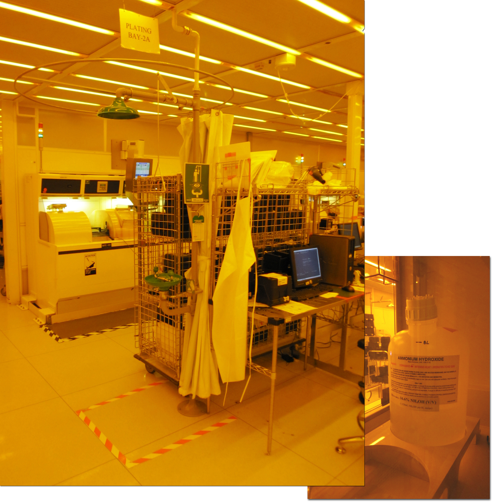
These showers may be co-ed, but they’re definitely no fun. Emergency showers show up throughout the wafer fab cleanroom. Wherever there are wet chemical processes, such as electroplating, wet etching, chemical-mechanical planarization, and so forth, emergency showers must be within range. Despite the fact that cleanroom suits may hold contaminants in, they don’t keep liquids out. A splash of ammonium hydroxide (or much worse) to the eyes can do serious damage. Electroplating tools, for example, use a lot of acid. While the employee is getting doused in the shower, co-workers will call for an Emergency Response Team. The odd thing is that while I see drainage for the eye wash bowl, and that shower curtain pulls in a circle around the overhead shower head, I don’t seen any drainage on the floor. Let’s hope those computer cords on the floor nearby are waterproof.
Ion Beam Deposition
Ion beams can be used as yet another method of depositing a very fine layer of material on a surface. A gas is subjected to very high electric fields, leading to ionization. The IBD tool uses very high voltage to focus and accelerate the beam of ions toward a substrate and then, optionally, decelerate it to better control the deposition. In WD’s case, this IBD tool is used to process the junction portion of the reader block. This is the critical point where the reader’s electrical and magnetic connectors meet with the TMR stack. Thickness, junction angle, and the precise material composition are controlled extremely tightly at this step.
Got You Tagged
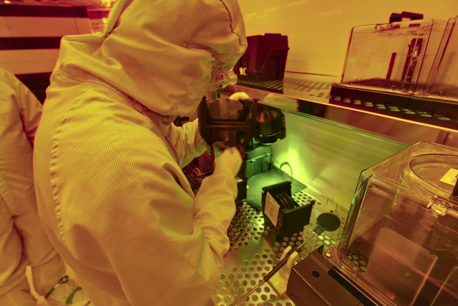
Incredibly, a single six-inch wafer yields about 50,000 “sliders.” Not only does the wafer get its own unique ID number, so does each slider. The slider ID indicates both the wafer ID as well as its own row and column position within the wafer. For quality control purposes, each slider is required to be 100% traceable. Here, you can see a wafer fab operator inspecting a wafer identification number. Perhaps I’d been in the yellow world for so many hours at this point that the green light used to help the operator see the ID numbers called to me like a blue bug zapper to a moth. I just hovered around it for a while, enjoying the fact that it wasn’t yellow. You can see a video of the operator at work here.
-
zelog I'm guessing the metal plate on the floor in picture 29 is slightly elevated to let the water drain.Reply -
johnbilicki There are a lot of DOA complaints on Newegg and even with 40% of that place is required to make sure the drive works before it leaves the building it still has to go through shipping...UPS shows up eight hours after FedEx and the drive it dead because during shipping your package was the substitute baby for 'kick the baby'.Reply -
milosz It's amazing that all this precision work and exotic manufacturing technology can be had for $150Reply -
anamaniac Awesome. =DReply
I've switched to Samsung drives though. ^_^
And at the pic on page 26, she's checking her farmville. (At my job we hired an insanely expensive technician to fix some really expensive equipment, which he did with his laptop... and he has checking his farmville... at a few hundred dollars per hour on the company dime of course.)
Interesting that there appeared to be no drainage for the emergency shower. They just jerry rig that thing up at the last moment and hope no one has to use it?
Also, that walkthrough video is quite depressing. Yellow rooms as far as the eye can see, without a smile in sight.
Thank you very much for this wonderful article. As much as I'd like to, I doubt I could ever work there, because my handa aren't stable enough just to take a damned picture, nevermind handle extremely precise equipment. =)
But I wonder, how many drive failures have they had because an employee dropped a contact into the drive?
Also, great to see that little sneak preview on WD NAND based storage.
Now, how about Intel and 32nm? -
kikireeki And a new HDD is born and it is DOA! "sarcasm"Reply
I just hope that WDD has done it right this time! -
jhanschu I'm under the assumption that most of the pictures were taken in a "clean room" environment. As such, the floor grating would be elevated (as previously mentioned) for the laminar air flow and there may possibly be a drain below. Also if I noticed correctly, the ceiling "tiles" were actually HEPA filters.Reply -
g00ey I'm not buying that every step visualized on these photos are being applied to each and every platter that is manufactured on this facility. For example I don't think they examine the layers of every platter in the TEM. I believe the photos don't only show the manufacturing line but also some of the research facilities for next generation products.Reply
I think the manufacturing process is very much like an assembly line process where the production flow is rather fluent which is not the impression I get at a first glance when looking through these photos. They obviously achieve som degree of economies of scale. It would be interesting too see some figures such as how long it takes to produce a platter, head, and so on and how many units/components per hour that is being produced etc.
Then look at for example picture 28 (or 25-32); I don't understand how these large electoplated platters turn into read/write heads of a harddrive. I don't see the part where these wafers are punched into small needles (sliders/heads) and how this is done. -
neiroatopelcc I find it marvelous to see all this expensive hightech and amongst those things find old crt monitors and I think in one picture about #20 I even spotted an old hp dx2000 in the right side of an image (in front of an older 13" or so crt. Really nice to see expensive mashinery associated with expensive downtime being operated using windows antique and old hardware. Seems you don't always NEED a quadcore to be effective.Reply
Great article btw. Not sure I share the authors humor, but I suppose it beats kevins.
