LCD Juggernaut: Tom's Hardware Looks Into Samsung's Seoul
Enter The Tiger*
After our photo tour inside Western Digital proved so popular with readers, we asked around to other vendors, looking for similar opportunities. So when Samsung invited Tom’s Hardware to send a journalist on a small press and analyst tour of its LCD manufacturing facilities in Tangjeong, South Korea, we jumped at the chance. Who in their right mind wouldn’t be excited to go? With so much change happening in displays now—240 Hz refreshing, AMOLED breakthroughs, the rise of 3D, and displays big enough to practically fill a wall—imagine being able to take a first-ever look inside where many of these technologies are created!
* The tiger is South Korea’s national animal.
The Hungry Giant
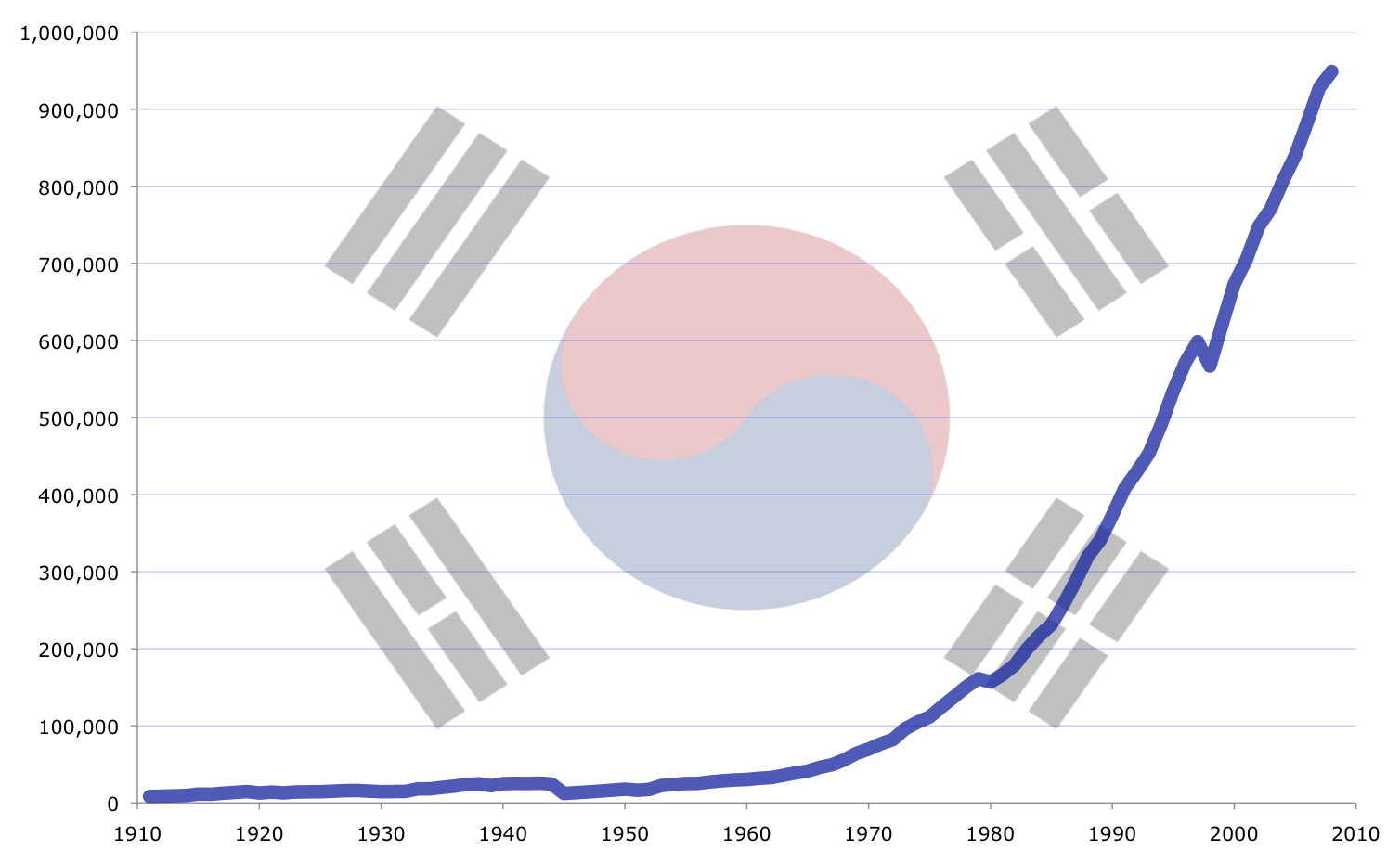
I love to travel, and I’d never been to the Korean peninsula before. So in any trip of this nature, it’s difficult to completely separate the technical experiences from the cultural and corporate ones. As an observer, they tend to blend together. You have to start this trek with knowing that the Korean War of 1950 to 1953 decimated both sides, leaving South Korea to flounder economically. According to my tour guide and Samsung assistant PR manager for LCDs, Jenny Ahn, after the war, South Korea had the lowest gross domestic product (GPD) per capita in the world. The land was shattered almost beyond recognition.
This was only 50-some years ago, within the memories of the country’s current industrial and political rulers. They remember war, hunger, and extreme poverty. While the subject was never discussed much in our group, the sense I got during my four days of travel within and around Seoul is that this is a country united by incredible determination never to return to those days or anything remotely like them. The people are skilled, motivated, and hungry for more. Much more. Quickly. And to get it, they’re ready to create and deliver the electronics gadgetry you’ve been dreaming of.
The New Company Store
As I pointed out in my recent Samsung photo story on Tom’s Guide, Samsung currently generates 13% of South Korea’s GDP. The company is practically a country within a country. Many of the workers at Samsung’s factories (as well as those at other industrial companies) live in massive dormitory complexes near the major fab facilities, some of them large enough to be cities in their own right. And even these complexes look feeble compared to the next generation of accommodations. Compare the 20-story buildings shown here with the skyscrapers recently finished in Tangjeong’s TraPalace complex. See here.
Samsung owns those dorm-cities, and employees pay only $30 per month to live in them. Samsung erected the buildings with its own construction company. Most if not all of the workers are covered by Samsung's own insurance company. You get the idea. This is a massive, vertically-integrated company the likes of which haven’t existed in the West for many decades.
An Apparently Content Army
As we bussed along the South Korean freeways, passing these complexes every so often, I found myself at first repulsed by the mountains of faceless, Spartan concrete.
Get Tom's Hardware's best news and in-depth reviews, straight to your inbox.
Then I had to forget that I come from America, with its “American Dream” of homeownership and affluence.
Viewed through the filter of efficiency, the South Korean approach is a brilliant system. The alternative would be a three-hour commute from Seoul, leaving employees reduced to only seeing their families on weekends (as many commuters in America do now) and coping with haphazard attendance. Shuttling people to and from work is done quickly and easily, and we were told they work in eight-hour shifts.
Compared to 60 years ago, these conditions are affluent, complete with schools, medical centers, and sports facilities. Indeed, as we mulled among the crowds of youthful fab laborers, they chatted happily and were dressed in tasteful, modern fashions. Many apparently drive their own cars, as the expansive parking lot was brimming with white, gray, and black vehicles. Interestingly, South Koreans seem not to buy cars painted in colors. I observed this while overlooking the Tangeong fab’s parking lot and confirmed it on Google Maps, as you can see in the center frame shown here. This perhaps unconscious display of uniformity reinforced my impressions about the culture and its cohesive mission.
From Ramshackle To Unshackled
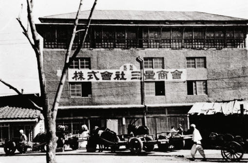
Strange but true: Samsung started in 1938 as a trading company specializing in dried fish and produce. Not until the late 1960s, when South Korea’s government decided to get serious about building a global-scale electronics industry, did Samsung enter the display market with its first product: a black and white TV.
Between then and now, you already know some of the history. Samsung grew and grew, thanks in part to the South Korean government keeping out foreign competition during the company’s formative years. Unfair? Maybe. Effective? Obviously. The company built its first LCD screen in 1995. Ten years later, it was the #1 LCD supplier in the world.
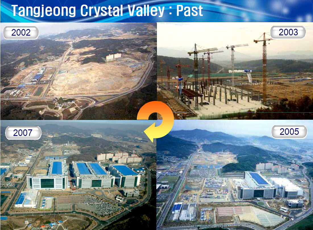
Tangjeong Past
In California, we have the Silicon Valley. In flattering imitation, Samsung has its Crystal Valley located in Tanjeong, roughly 50 miles south of Seoul. If the world had a center of LCD manufacturing, this would be it. Yet, as you can see, just eight years ago, there was nothing here but cleared land and a couple of initial dormitory buildings.
By 2007, four LCD fab lines were up and running. Each of these lines produces a specific generation of “mother glass,” the sheets from which smaller display panels are cut. Samsung notes these as “L” fab lines, which generally correspond to the same generation number. The most current line is L8.
Tangjeong Today
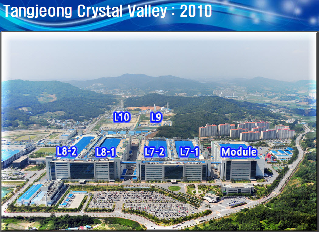
This is the Crystal Valley now, more or less as I saw it in person. Interestingly, Samsung notes that it now plans to skip the L9 and L10 lines/generations and leap clear to L11, which will measure 3.32 x 3.0 meters and yield six 60 inch or greater panels. Samsung didn’t care to discuss the subject beyond that point.
I’ll let Samsung’s Jenny Ahn describe the current facilities in her own words:
“The Tangjeong complex includes the world's first seventh-generation production lines, lines 7-1 and 7-2. The S-LCD 7-1 line, a joint venture with Sony, is mainly manufacturing 40" and 46" panels for LCD TVs. The 7-2 line, an exclusive production line for Samsung, makes use of the same size glass substrate for TV panels (1870 x 2200 mm). This fall, an eighth-generation S-LCD line will commence operations, adding 50 000 mother glass substrates (each measuring a record 2200 X 2500 mm) to the joint venture’s overall monthly production capacity. The eighth-generation fabrication line will mainly produce LCD panels for 52" diagonal or larger LCD TVs.”
Size Matters
| L1 | G2 | 370X470 |
| L2 | G3 | 550X650 |
| L3 | G3.5 | 600X720 |
| L4 | G4 | 730X920 |
| L5 | G5 | 1100x1250 |
| L6 | G5 | 1100x1300 |
| L7 (L7-1$L7-2) | G7 | 1870x2200 |
| L8 (L8-1-1&L8-1-2&L8-2-1) | G8 | 2160x2400 |
Just as chip manufacturers race for superior speed, LCD manufacturers race for superior size. The Samsung Corning Precision Materials (SCP) facilities, located right across the way from the L8-2 fab, is one of the top glass substrate manufacturers in the world, and the weight of supplying ever larger mother glass sheets at high yield levels falls on this group’s shoulders.
Why is this so important? Because the world wants bigger and bigger panels. As you can see in this iSuppli data, the days of sub-20" TVs and sub-17" monitors are about over. Market growth going forward clearly swings toward the larger sizes, and if the object of the cost game is to cut as many panels as possible from one pane of mother glass, then that better be one big mother in order to keep per-panel costs low.
Don’t Breathe
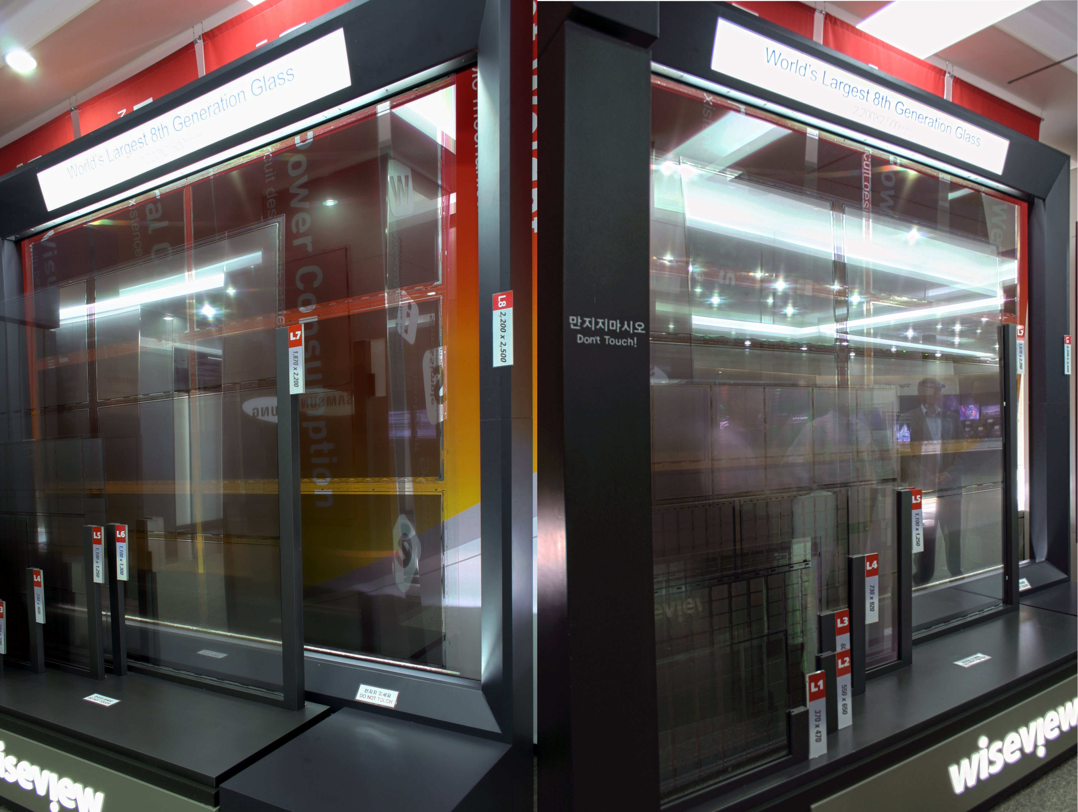
Skipping ahead slightly, I want to show you what these mother glass sheets have looked like over time. As a rule, Samsung says that the longest dimension of one mother glass generation should be the shortest dimension of the next. For example, an L7 pane measures 1870 x 2200 mm, or 74 x 86.6 inches. Moving to L8, that long edge now becomes the short edge, as L8 measures 2200 x 2500 mm, or 86.6 x 98.4 inches.
Samsung allegedly never allows people to touch its mother glass samples, but Jenny was allowed to grant us a rare exception. I pinched the L8 sheet, which is only 0.7 mm thick, between my thumb and forefinger and gave the pane a slight wiggle. The sensation was similar to handling a sheet of paper laminated in plastic. The glass is so unbelievably thin that it just flexes and wiggles, easily warping and bouncing back when you let go. I instinctively withdrew my hand quickly, afraid that just a bit more pressure or movement would shatter the substance. After all, glass is supposed to be rigid. I’d never seen anything like this before.
Through The Gate
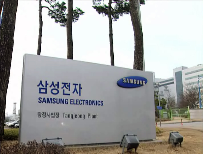
In a country where most of the trees around buildings seem to be about four inches in diameter and still propped up with sticks or boards because nothing has had time to take root yet, aesthetics sometimes have to wait. This plain sign is all that greets visitors to the Tangjeong facility as they pull in.
Honestly, I didn’t even notice it at first. I was too busy staring open-mouthed at the manufacturing facilities. In the back of my head, the geek in me wanted to whisper, “That’s no fab. It’s a space station.” I knew that the first three L7 lines crank out 130 000, 150 000, and 70 000 panels per month while the two L8 lines each contribute 100 000 panels monthly. Nearly all of this volume goes to TV screens. I knew those were big numbers, but I didn’t really grasp what sort of infrastructure was needed to achieve those numbers....
The L8th Wonder Of The World
These images do no justice to the immensity of the Tangjeong buildings. I’ve stood before the Great Pyramid of Giza and didn’t feel even half as dwarfed as I did staring up at the L7 and L8 structures. The Great Pyramid measures about 756 feet per side at its base. I don’t know what the fab’s dimensions are, but you can get some idea from the size of those tiny people in the left picture.
Some incredible factoids I did learn: The Tangjeong complex employs about 20 000 people. Thirty percent are in R&D, 60% are fab workers. The entire complex occupies about 4.8 million square meters, of which only 1.5 million have been used so far. And the L7 and L8 line pairs each cost almost $6 billion USD. This is staggering when you consider that the price tag for a new 300 mm CPU wafer fab is $2.5 to $3.5 billion.
-
p1n3apqlexpr3ss Wow... south korea from nothing to one of the most technologically advanced countries in the world some could argue in just over 50 years, with plants like these and also with the fastest broadband connections...Reply
Nice article as usual as well, pity bout the actual manufacturing floor and filming stuff though :( -
one-shot Wow.....Reply
It's amazing what goes into a factory of this enormous scale.
Did anyone notice the garage doors in the side of the Fabs in the larger pics? It looked like garage doors in the sides several stories up. Good thing this isn't a Foxconn factory. -
rohitbaran Picture 6 shows how fast Koreans can develop a region. Magnificent facility. I admire their dedication as much as I can perceive from this virtual tour.Reply -
rohitbaran So, Sony working with Samsung (7th picture)! Well, maybe it would be useless to compare LCDs then!Reply -
amnotanoobie rohitbaranSo, Sony working with Samsung (7th picture)! Well, maybe it would be useless to compare LCDs then!Reply
It's not unusual for them to outsource some of their production to the largest producer of LCD's. Probably though, some of their higher-end or newer models may still be made by Sony itself. -
rohitbaran ReplyI recall passing one normally illuminated area in which test patterns were examined by lines of technical staff, with the control systems running Windows XP.
Ha ha. Proves something about XPs popularity, an OS that refuses to die despite its creator's sincere efforts. -
rohitbaran BTW, the title of the article should have been "LCD Juggernaut: Tom's Hardware Looks Into Samsung's S(e)oul"Reply
