The History Of Intel CPUs: Updated!
Bonnell: Airmont
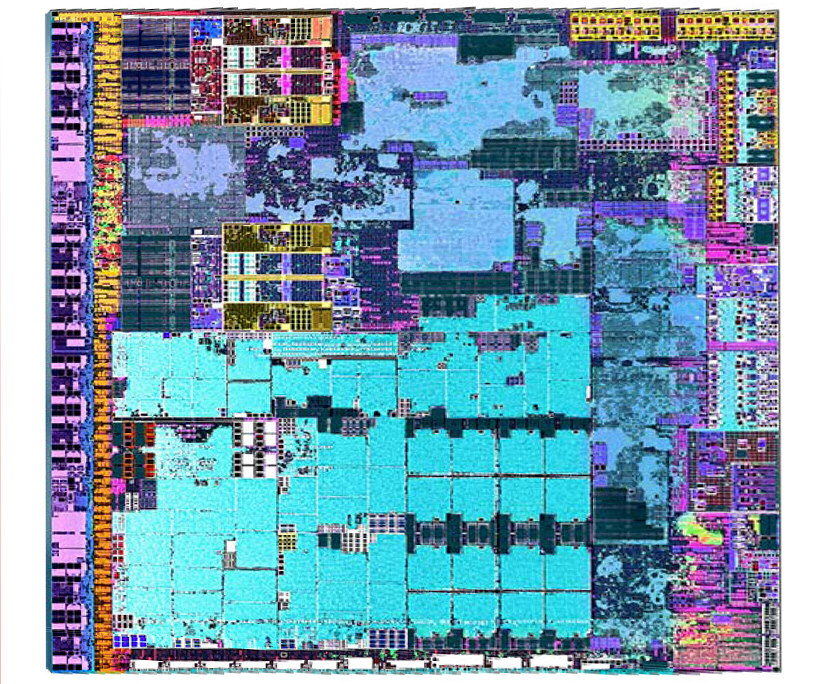
With its 14nm fab up and running, Intel did not hesitate to push out a new Atom chip built from these transistors. This CPU die was essentially a shrink of Silvermont, and Intel named it "Airmont." It did not improve IPC, but thanks to the die shrink it still managed to somewhat outperform its predecessor. After all, the move to 14nm transistors reduced heat dissipation, allowing the CPU to maintain its Turbo Boost frequency for longer periods of time.
Airmont's iGPU was significantly improved over Silvermont. The die itself contains 24 EUs, but products based on Airmont use between 12 to 16. None of the models based on Airmont currently all 24 EUs, and we are unlikely to see one in the future. These extra eight EUs exist to improve yields of Airmont, as a larger portion of the chip can be defective and still be salvageable. The graphics architecture was also updated to Intel's eight-gen Broadwell, improving the EUs' performance.
Airmont products were sold under the "Cherry Trail" and "Braswell" code names. The fastest Airmont-based Atom CPU is the N3700, which contains four CPU cores clocked at 1.6 GHz with a Turbo Boost frequency of 2.4 GHz. It also has a dual-channel DDR3L memory controller and 16 EUs clocked at up to 700 MHz.
Skylake
In 2015, not long after Broadwell first showed up on desktop systems, Intel replaced Broadwell with its Skylake architecture. Although Skylake-based CPUs were Intel's fastest to date, the platform changes accompanying Skylake were arguably more important.
Skylake was the first consumer-oriented CPU to use DDR4 memory, which is more energy-efficient than DDR3 and capable of enabling greater throughput. The Skylake platform also contained a number of improvements, such as a new DMI interface, an upgraded PCIe controller, and support for a much wider array of connectivity devices.
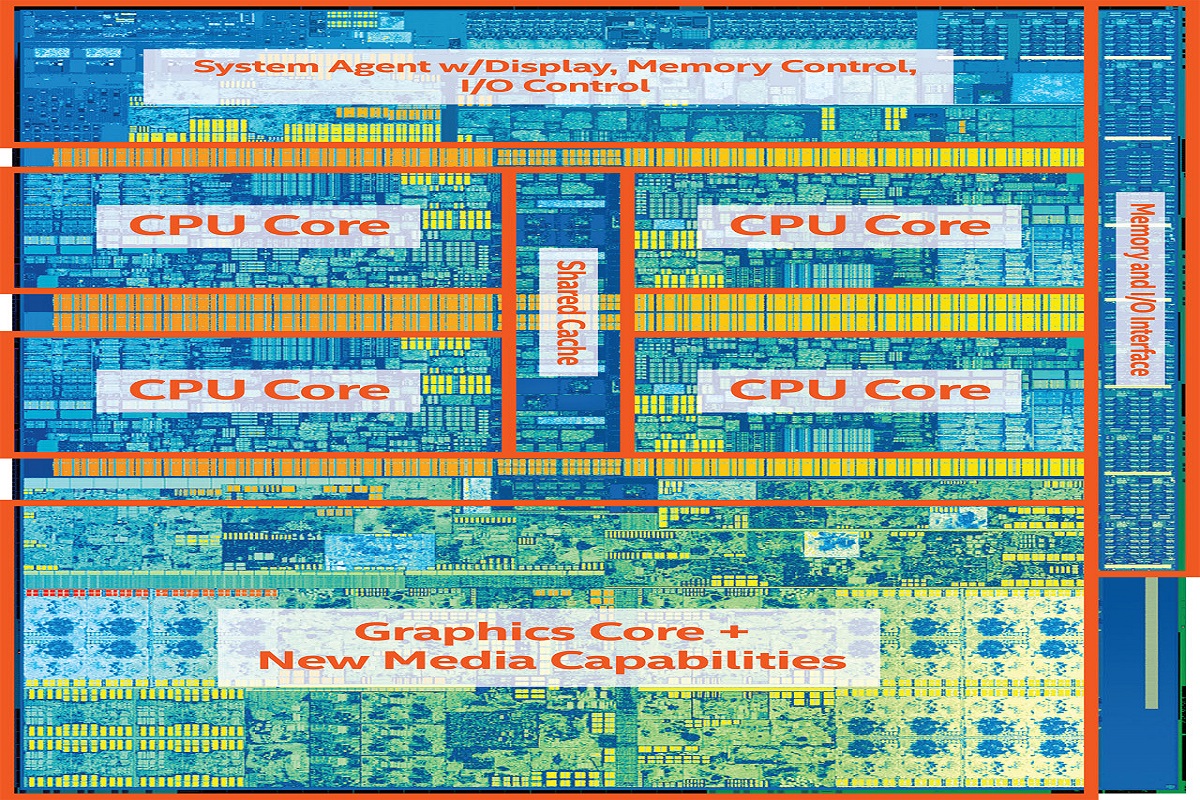
Naturally, Skylake included a better on-die GPU as well. The highest-end model was known as Iris Pro Graphics 580, and it was deployed to certain Skylake-R CPUs. The Iris Pro Graphics 580 engine featured 72 EUs and came paired with 128MB of L4 eDRAM. Most other Skylake-based chips included HD Graphics with 24 EUs, based on a design similar to Broadwell's.
Kaby Lake
Starting with Skylake and Kaby Lake, Intel ended its tick-tock development cadence in favor of a tick-tock-tock schedule. It was also referred to as the process-architecture-optimize cadence. This extended the amount of time Intel spent on a single fabrication process before it developed a new one. It also extended the amount of time between major architectural changes.
Get Tom's Hardware's best news and in-depth reviews, straight to your inbox.
Kaby Lake, therefore, was essentially an optimized variation of Intel’s Skylake architecture. Although still 14nm, Intel utilized a process it called 14nm+ that had various tweaks to improve energy efficiency and performance. The architecture itself hardly changed at all, but it did facilitate DDR4-2400 memory support.
Kaby Lake also employed an HD Graphics 630 engine featuring improved codecs for encoding and decoding, extending support for 4K video playback.
Coffee Lake
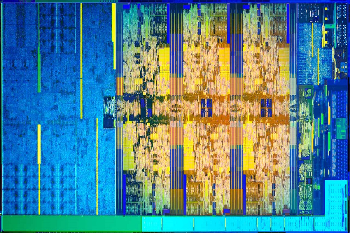
With Coffee Lake, Intel increased the number of cores in its Core i3, i5, and i7 processors by two. This marked the largest increase in core count for Intel since the introduction of the Core 2 Quad in 2006.
Core i5s now have six cores without Hyper-Threading. Coffee Lake-based Core i7s also have six cores, but with Hyper-Threading. The underlying architecture does not change from Kaby Lake. However, with more cores to share the work, performance increases markedly in threaded applications.
Coffee Lake-based Core i3 processors lack Hyper-Threading, but thanks to the increase from two to four CPU cores, the Core i3 processor family has never wielded more power. In essence, Coffee Lake Core i3 CPUs are every bit as powerful as Kaby Lake Core i5s, and potentially faster than Skylake Core i5s.
Whiskey Lake and Amber Lake
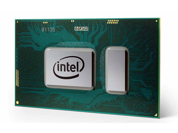
Intel's delayed 10nm process has slowed progress on the smaller Cannon Lake processors, so the company developed the 14nm++ Whiskey Lake and 14nm+ Amber Lake processors for laptops, to fill the gap between generations.
The new 15-watt U-Series Whiskey Lake models slot into the same Eighth Generation Core “Kaby Lake-R” product stack as previous-generation mobile chips, and have the same numbers of cores and threads as the chips they’ll be replacing. And the 5-watt Amber Lake models replace the seventh-gen Y-series chips found primarily in fanless laptops and convertibles. One of the primary new features for Whiskey Lake is the addition of the first hardware-based fixes for Meltdown and L1TF to appear on consumer-focused CPUs.
The Whiskey Lake and Amber Lake processors all feature the same underlying Kaby Lake microarchitecture as previous-generation CPUs, with a few optimizations. Primarily, single-core boost frequencies get a big bump over previous parts (up to 4.6GHz with the Core i7-8565U). But of course, exactly how long your CPU will stay at that top speed depends largely on the device’s cooling abilities.
MORE: Best CPUs
MORE: Intel & AMD Processor Hierarchy
MORE: All CPU Content
-
abryant Archived comments are found here: http://www.tomshardware.com/forum/id-3322311/history-intel-cpus.htmlReply -
mitch074 Strange that Itanium is missing, the Celeron 300A/333 is gone, the original Pentium bug disappeared, no mention is made that the 487 was actually a fully active 486DX, and that AMD led the desktop for "a short time" while it led from the moment Netburst came out (2000) to the moment Core replaced it (2006). On another note, a 64-bit CPU doesn't run 64-bit software faster : it is required to have one to run some. But since AMD came up with x86-64, I guess some approximation is allowed...Reply -
Tom Griffin Remember the ABIT BP6a motherboard; I was running dual Celery (Celeron) 300mhz processors overclocked to 533mhz. What a flashback.Reply -
AndrewJacksonZA 1) Where can we see what was updated please?Reply
2) Where are the Phi CPUs please?
3) Where can we view this as a one-pager please? -
ta152h There are quite a few mistakes here.Reply
For one, the 8086 was not available in higher clock speeds than the 8088.
The 8086 could NOT run 8080 code. Source code compatible does not mean that. It means it was very easy to recompile the code so it would work with the newer processor, not that the compiled code would work.
The 286 section is oddly very limited. It was an enormous improvement over the 8086, as it added more memory, much more performance, and also virtual memory and hardware assisted multi-tasking.
The 80386 was not significantly faster than the 286 running 16-bit code, despite what the author says. Clock for clock, they were very close, although 386 based systems tended to get SRAM caches, whereas the 16 and 20 Mhz 286s rarely did.
The 386SX not only cut down the data bus to 16 bits, it also cut down the address bus to 24-bits.
The remarks on the i860 are bizarre. " ... it was nearly impossible to correctly list every instruction from beginning to end when compiling the program. " This is wrong, it was just very difficult to order the instructions very efficiently. Of course it had no problem listing them correctly, or the program wouldn't run. Intel tried it again with Itanium, and depended on the compilers to order instructions very efficiently, and also had difficulties.
The author oddly left out the most significant part of the 486; it was the first pipelined x86 CPU, and that was a large part of the performance improvement.
The Pentium's FPU was not 10x faster than the 486, but it was the biggest improvement. Unless you're comparing a very low clocked 486 to a high clocked Pentium. Clock per clock, it was not nearly 10x faster.
Also MMX instructions were not related to the FPU, but were actually integer based.
The first Pentiums actually ran at 66 MHz, but ran really hot, and they had yield problems, so sold 60 MHz Pentiums along with them, at a significant discount. Most people bought the 60 MHz because they were so much cheaper initially, but 66 MHz was out there.
The Pentium MMX only reached 233 MHz as sold by Intel, not 300 MHz.
The Pentium III (Katmai) was a Pentium II with SSE instructions added, nothing more. The nonsense about fewer pipelines and IPC improvements (outside of SSE code) is fabricated with regards to Katmai.
The Celeron originally had no cache, but there was another version (not a Coppermine based) that had 128K cache on the processor. In some ways, it was faster than the Pentium III it was based on, because the cache was faster.
Coppermine's cache was wider, and generally superior, but Celeron's were very competitive with Katmai based products, and were the favorites of overclockers. -
mitch074 Reply21307316 said:The Celeron originally had no cache, but there was another version (not a Coppermine based) that had 128K cache on the processor. In some ways, it was faster than the Pentium III it was based on, because the cache was faster..
The Celeron 300A/333 you're referring to is the Mendocino core, wasn't based on Pentium III - it didn't have support for SSE. It can be seen as a precursor for Pentium III inasmuch as it had 128 Kb of level 2 non-inclusive low-latency cache - and it was the first Intel P6-family CPU to have that.
It was soon replaced with the Coppermine core, which was indeed based on the Pentium III core (SSE) as it was a smaller die (smaller engraving) thus much cheaper to produce. -
milkod2001 Still on Haswell 4770k. Don't see any reasons to upgrade apart from m.2 SSDs maybe but have regular SATA SSD and there might be no difference in actual performance. Right?Reply
