The History Of Intel CPUs: Updated!
Bonnell: Silverthorne And Diamondville
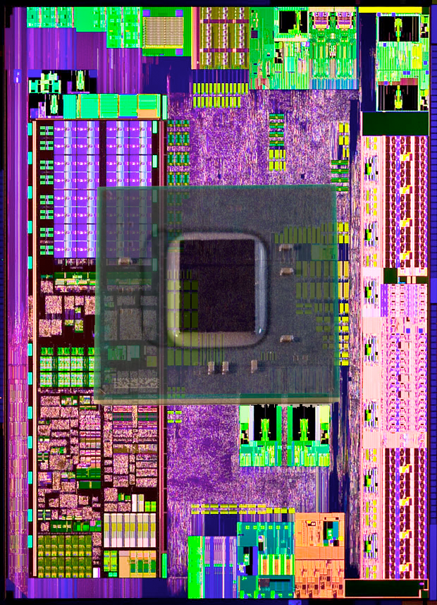
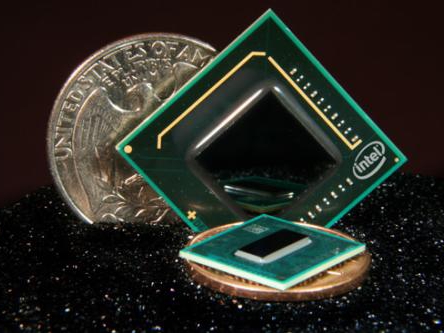
The Core 2 architecture hit a wide range of devices, but Intel needed to produce something less expensive for the ultra-low-budget and portable markets. This led to the creation of Intel's Atom, which used a 26mm2 die, less than one-fourth the size of the first Core 2 dies.
Intel didn't design Atom's Bonnell architecture completely from scratch, but instead went back to the Pentium's P5 foundation. That was largely because P5 was Intel's last in-order execution design. OoO execution, though highly beneficial to performance, also consumes quite a bit of power and takes up a large amount of die space. For Intel to meet its goals, OoO simply wasn't practical at the time.
The first Atom die, code named "Silverthorne," had a TDP of 3W. This enabled it to go places that Core 2 could not. Silverthorne's IPC was lackluster, but it was able to run at up to 2.13 GHz. It also contained 512KB of L2 cache. The decent frequency and L2 cache did little to make up for the low IPC, but Silverthorne still enabled an entry-level experience at a relatively low price.
Silverthorne was succeeded by Diamondville, which reduced the frequency to 1.67 GHz but enabled 64-bit support, which improved performance in 64-bit apps.
Nehalem: The First Core i7
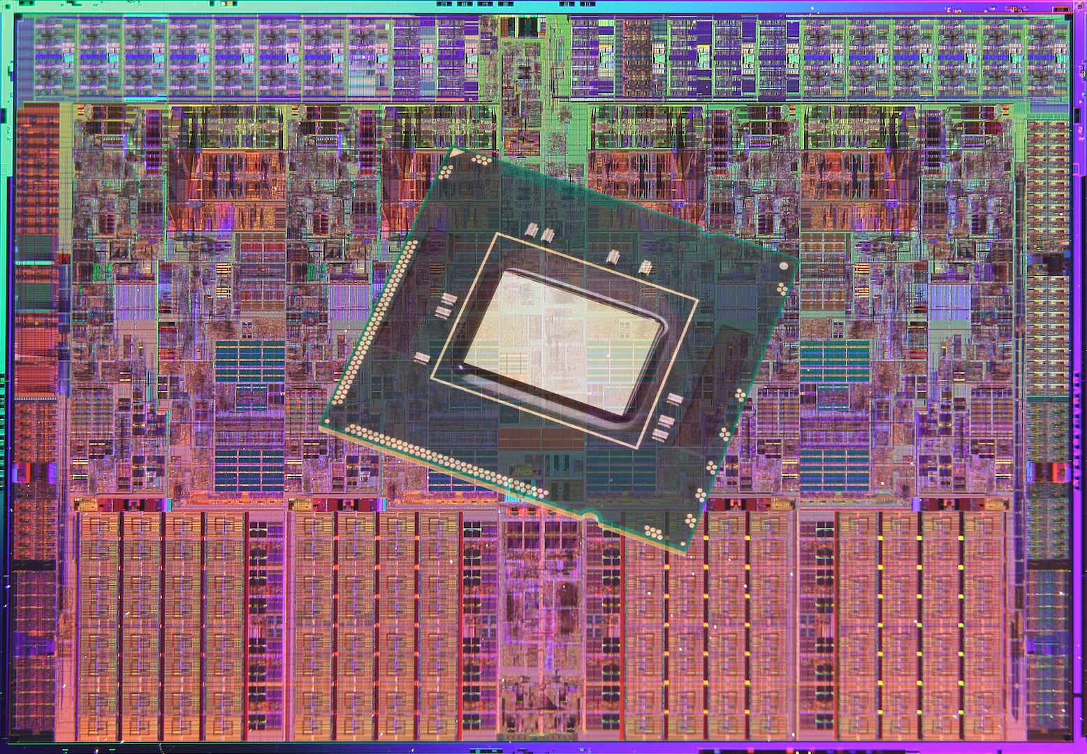
With the processor market in a highly competitive state, Intel couldn't afford to sit still for long. So, it reworked the Core architecture to create Nehalem, which adds numerous enhancements. The cache controller was redesigned, and the L2 cache dropped to 256KB per core. This did not hurt performance though, as Intel instead added between 4-12MB of L3 cache shared between all of the cores. CPUs based on Nehalem included between one and four cores, and the family was built using 45nm technology.
Intel significantly reworked connections between the CPU and rest of the system as well. The ancient FSB that had been in use since the 1980s was finally put to rest, and it was replaced by Intel's QuickPath Interconnect (QPI) on high-end systems and by DMI everywhere else. This allowed Intel to move its memory controller (which was updated to support DDR3) and PCIe controller into the CPU. These changes significantly increased bandwidth while latency plummeted.
Once again, Intel extended the processor pipeline, this time to 20-24 stages. Clock rates did not increase, however, and Nehalem ran at comparable frequencies to Core. Nehalem also was Intel's first processor to implement Turbo Boost. Although the fastest Nehalem processor's base clock topped out at 3.33 GHz, it could operate at 3.6 GHz for short periods thanks to this new technology.
Get Tom's Hardware's best news and in-depth reviews, straight to your inbox.
The last major advantage that Nehalem had over the Core architecture was that it marked the return of Hyper-Threading technology. Thanks to this and numerous other enhancements, Nehalem was able to perform up to twice as fast as Core 2 processors in heavily-threaded workloads. Intel sold Nehalem CPUs under the Celeron, Pentium, Core i3, Core i5, Core i7, and Xeon brands.
Bonnell: Pineview And Cedarview
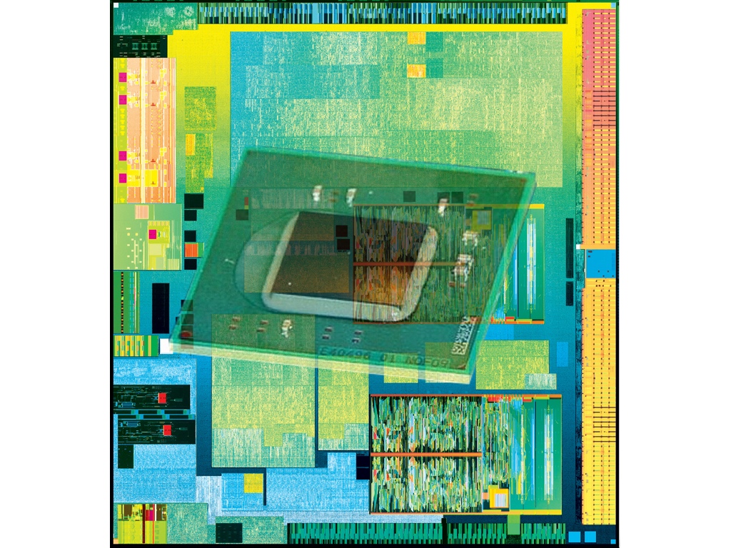
In 2009, Intel released two new Atom-branded dies based on the Bonnell architecture. The first was known as "Pineview," which continued to use a 45nm fabrication process. It featured better performance than Diamondville by integrating a number of components traditionally found inside of the motherboard chipset, including graphics and the memory controller. This had the effect of reducing power consumption and lowering heat dissipation. Dual-core models were also available using two Pineview cores on an MCM.
Westmere: Graphics In The CPU
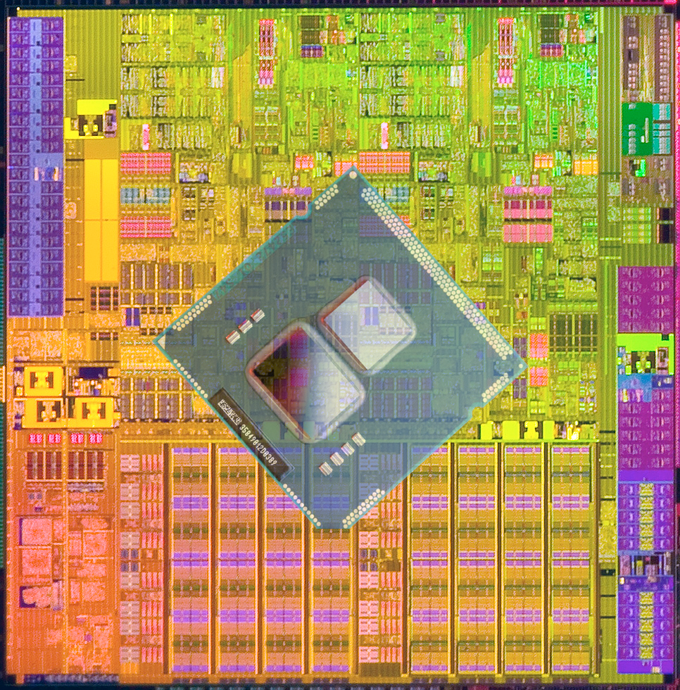
Intel created a 32nm die shrink of Nehalem that was code-named "Westmere." Its underlying architecture changed little, but Intel took advantage of the reduced die size to place additional components inside of the CPU. Instead of just four execution cores, Westmere contained up to 10. It could also have as much as 30MB of shared L3 cache.
The HD Graphics implementation in mainstream Westmere-based Core i3, i5, and i7 processors was similar to Intel's GMA 4500, except it had two additional EUs. Clock rates stayed about the same, ranging between 166 MHz in low-power mobile systems and 900 MHz on higher-end desktop SKUs. Although the 32nm CPU die and 45nm GMCH weren't fully integrated into a single piece of silicon, both components were placed onto the CPU package. This had the effect of reducing latency between the memory controller inside of the GMCH and the CPU. API support didn't significantly change between the GMA and HD Graphics implementations, though overall performance increased by over 50 percent.
Related: Evolution of Intel Graphics: i740 To Iris Pro
Sandy Bridge
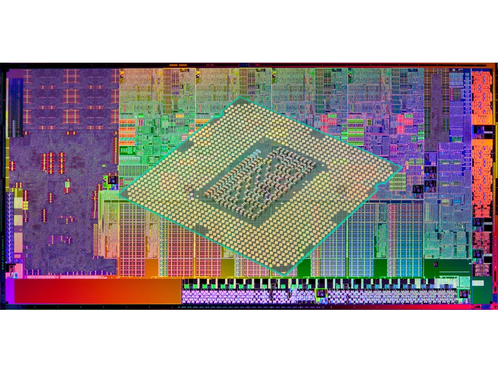
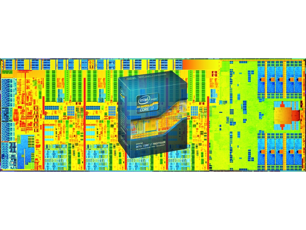
With Sandy Bridge, Intel made its most significant leap in performance, the most in seven years. The execution pipeline was shortened into 14-19 stages. Sandy Bridge implemented a micro-op cache capable of holding up to 1500 decoded micro-ops that enabled instructions to bypass five stages if the micro-op required was already cached. If not, the instruction would have to run the full 19 stages.
The processor also featured several other improvements, including support for higher-performance DDR3. More components were integrated into the CPU as well. Instead of two separate dies on the CPU package (as on Westmere), everything moved into one die. The various subsystems were connected internally by a ring bus that enabled extremely high-bandwidth transactions.
Intel again updated its integrated graphics engine. Instead of a single HD Graphics implementation pushed into all CPU models, the company created three different versions. The top-end variant was the HD Graphics 3000 with 12 EUs that was could be clocked up to 1.35 GHz. It also contained extras like Intel's Quick Sync transcoding engine. The mid-range HD Graphics 2000 variant possessed the same features, except it dropped down to six EUs. The lowest-end HD Graphics model also had six EUs, but with the value-added features.
Bonnell: Cedarview
In 2011, Intel created another new Atom die based on the same Bonnell architecture used inside of Pineview. Again, there were minor core enhancements to improve IPC, but in reality little changed between the two. Cedarview's key advantage was a move to 32nm transistors that enabled frequencies up to 2.13 GHz at lower power. It was also able to support higher-clocked RAM thanks to an improved DDR3 memory controller.
Ivy Bridge
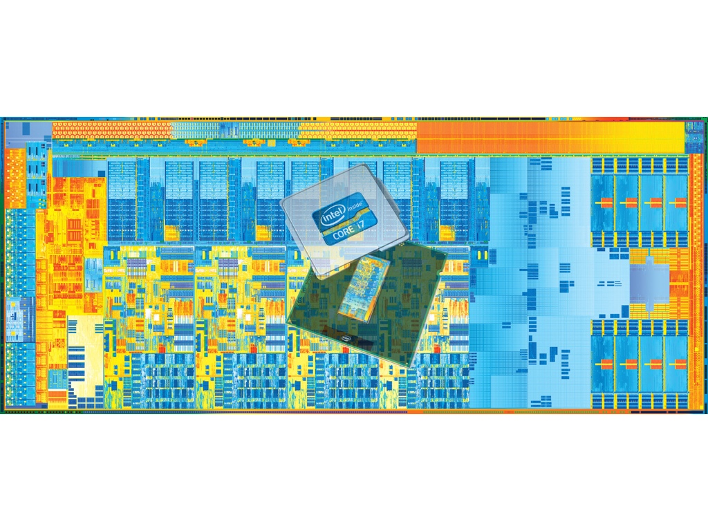
Intel followed Sandy Bridge with its Ivy Bridge processors, a "Tick+" in the company's "Tick-Tock" product design cadence. Ivy Bridge's IPC was only slightly better than Sandy Bridge's, but it brought with it other key advantages that outshined its predecessor.
Ivy Bridge's greatest advantage was its energy efficiency. The architecture was crafted with 22nm three-dimensional FinFET transistors that sharply reduced the CPU's power consumption. Whereas mainstream Sandy Bridge-based Core i7 processors typically came with a 95W TDP, the equivalent Ivy Bridge-based chips were rated at 77W. This was particularly important in mobile systems, and it allowed Intel to release a quad-core mobile Ivy Bridge CPU with a low 35W TDP. Prior to this, all of Intel's quad-core mobile CPUs came with at least a 45W TDP.
Intel took advantage of the reduced die size to also enlarge the iGPU. Ivy Bridge's highest-end graphics engine, HD Graphics 4000, packed in 16 EUs. The graphics architecture was also significantly reworked to improve the performance of each EU. With these changes, HD Graphics 4000 typically performed 200 percent better than its predecessor.
Haswell
Like a metronome, Intel pushed out its Haswell architecture just one year after Ivy Bridge. Haswell was once again more of an evolutionary step than a revolutionary one. The AMD processors competing against Sandy and Ivy Bridge weren't fast enough to do battle at the high end, so Intel wasn't pressured to increase performance too much. Haswell was approximately just 10 percent faster than Ivy Bridge overall.
Similar to Ivy Bridge, Haswell's most attractive features were its energy efficiency and iGPU. Haswell integrated the voltage regulation hardware into the processor, which enabled the CPU to keep a better handle on power consumption. The voltage regulator caused the CPU to produce more heat, but the Haswell platform as a whole became more efficient.
To combat AMD's APUs, Intel placed as many as 40 EUs inside of its top-end Haswell iGPU. The company also sought to increase the available bandwidth its fastest graphics engine had access to by equipping it with a 128MB L4 eDRAM cache, which drastically improved performance.
Bonnell: Silvermont
In 2014, Intel significantly reworked the Bonnell architecture to create Silvermont. One of the most significant changes was a switch to an OoO design. Another was the elimination of Hyper-Threading.
When the Bonnell architecture debuted, many felt that OoO occupied too much die space and was too power-hungry for an Atom CPU. By 2014, however, transistors had shrunk to such a small size and enjoyed reduced power consumption significantly enough that Intel could enable an OoO design on Atom. Intel also reworked the pipeline in Silvermont to minimize the impact of a cache miss. These changes, combined with a number of other improvements, resulted in a 50 percent increase in IPC compared to Cedarview.
To further boost Silvermont's performance, Intel created SKUs containing up to four CPU cores. It also switched to an iGPU based on the same graphics architecture in its Ivy Bridge processors. There were only four EUs in Silvermont's iGPU, but it nonetheless was capable of providing 1080p video playback, and it could run older games that weren't especially taxing. All aspects of the chipset were integrated into the Silvermont CPU as well, but this was more to reduce the system power consumption than anything.
The Silvermont die was used in Bay Trail-based products. The platform's TDP ranges between 2 and 6.5W, and the clock rate ranges between 1.04 and 2.64 GHz.
Broadwell
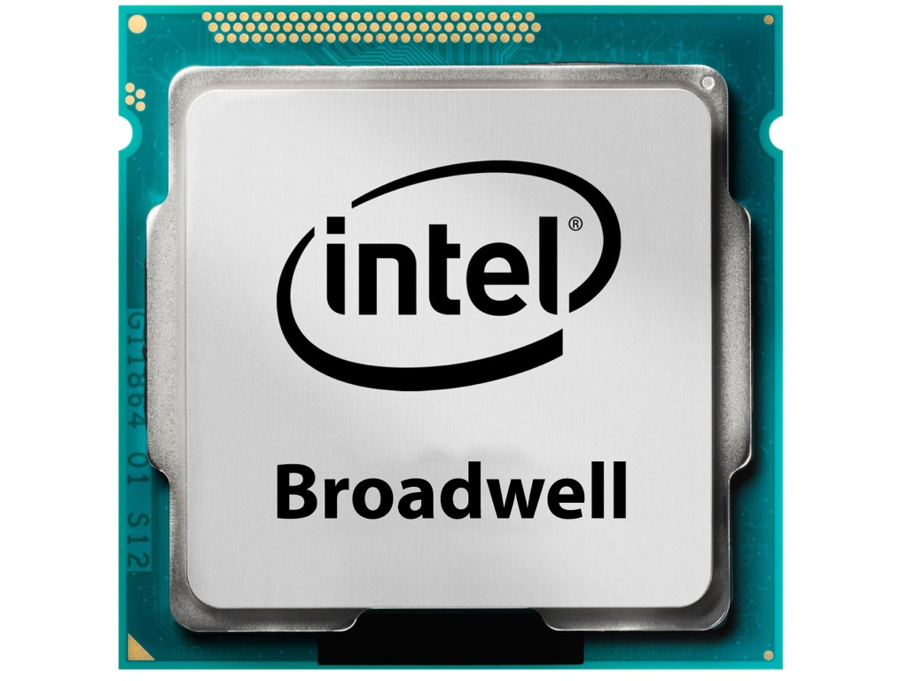
Intel's next processor architecture was known as Broadwell. Designed for mobile systems, it was released in late 2014 and used 14nm transistors. The first Broadwell-based product was called the Core M, and it was a dual-core Hyper-Threaded processor that operated with a 3-6W TDP.
Other mobile Broadwell processors dribbled out over time, but on the desktop side of the market, Broadwell never really showed up. A few desktop-oriented models were released in mid-2015. However, their reception was tepid. The highest-end SKU, however, contains the fastest integrated GPU Intel has ever added to a socketed CPU. It contains six subslices with eight EUs each, adding up to a total of 48. The GPU also has access to a 128MB L4 eDRAM cache, which helps to resolve the bandwidth challenges on-die graphics engines typically face. In gaming tests, it outperformed AMD's fastest APU and proved to be more than capable of providing playable frame rates in modern games.
-
abryant Archived comments are found here: http://www.tomshardware.com/forum/id-3322311/history-intel-cpus.htmlReply -
mitch074 Strange that Itanium is missing, the Celeron 300A/333 is gone, the original Pentium bug disappeared, no mention is made that the 487 was actually a fully active 486DX, and that AMD led the desktop for "a short time" while it led from the moment Netburst came out (2000) to the moment Core replaced it (2006). On another note, a 64-bit CPU doesn't run 64-bit software faster : it is required to have one to run some. But since AMD came up with x86-64, I guess some approximation is allowed...Reply -
Tom Griffin Remember the ABIT BP6a motherboard; I was running dual Celery (Celeron) 300mhz processors overclocked to 533mhz. What a flashback.Reply -
AndrewJacksonZA 1) Where can we see what was updated please?Reply
2) Where are the Phi CPUs please?
3) Where can we view this as a one-pager please? -
ta152h There are quite a few mistakes here.Reply
For one, the 8086 was not available in higher clock speeds than the 8088.
The 8086 could NOT run 8080 code. Source code compatible does not mean that. It means it was very easy to recompile the code so it would work with the newer processor, not that the compiled code would work.
The 286 section is oddly very limited. It was an enormous improvement over the 8086, as it added more memory, much more performance, and also virtual memory and hardware assisted multi-tasking.
The 80386 was not significantly faster than the 286 running 16-bit code, despite what the author says. Clock for clock, they were very close, although 386 based systems tended to get SRAM caches, whereas the 16 and 20 Mhz 286s rarely did.
The 386SX not only cut down the data bus to 16 bits, it also cut down the address bus to 24-bits.
The remarks on the i860 are bizarre. " ... it was nearly impossible to correctly list every instruction from beginning to end when compiling the program. " This is wrong, it was just very difficult to order the instructions very efficiently. Of course it had no problem listing them correctly, or the program wouldn't run. Intel tried it again with Itanium, and depended on the compilers to order instructions very efficiently, and also had difficulties.
The author oddly left out the most significant part of the 486; it was the first pipelined x86 CPU, and that was a large part of the performance improvement.
The Pentium's FPU was not 10x faster than the 486, but it was the biggest improvement. Unless you're comparing a very low clocked 486 to a high clocked Pentium. Clock per clock, it was not nearly 10x faster.
Also MMX instructions were not related to the FPU, but were actually integer based.
The first Pentiums actually ran at 66 MHz, but ran really hot, and they had yield problems, so sold 60 MHz Pentiums along with them, at a significant discount. Most people bought the 60 MHz because they were so much cheaper initially, but 66 MHz was out there.
The Pentium MMX only reached 233 MHz as sold by Intel, not 300 MHz.
The Pentium III (Katmai) was a Pentium II with SSE instructions added, nothing more. The nonsense about fewer pipelines and IPC improvements (outside of SSE code) is fabricated with regards to Katmai.
The Celeron originally had no cache, but there was another version (not a Coppermine based) that had 128K cache on the processor. In some ways, it was faster than the Pentium III it was based on, because the cache was faster.
Coppermine's cache was wider, and generally superior, but Celeron's were very competitive with Katmai based products, and were the favorites of overclockers. -
mitch074 Reply21307316 said:The Celeron originally had no cache, but there was another version (not a Coppermine based) that had 128K cache on the processor. In some ways, it was faster than the Pentium III it was based on, because the cache was faster..
The Celeron 300A/333 you're referring to is the Mendocino core, wasn't based on Pentium III - it didn't have support for SSE. It can be seen as a precursor for Pentium III inasmuch as it had 128 Kb of level 2 non-inclusive low-latency cache - and it was the first Intel P6-family CPU to have that.
It was soon replaced with the Coppermine core, which was indeed based on the Pentium III core (SSE) as it was a smaller die (smaller engraving) thus much cheaper to produce. -
milkod2001 Still on Haswell 4770k. Don't see any reasons to upgrade apart from m.2 SSDs maybe but have regular SATA SSD and there might be no difference in actual performance. Right?Reply
