The History Of Intel CPUs: Updated!
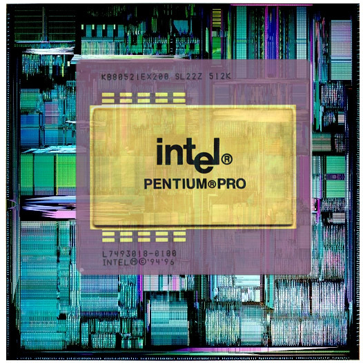
P6: The Pentium Pro
Intel planned to quickly follow the Pentium up with the Pentium Pro based on its P6 architecture, but ran into technical difficulties. The Pentium Pro was considerably faster than the Pentium in 32-bit operations thanks to its Out-of-Order (OoO) design. It featured a significantly redesigned internal architecture that decoded instructions into micro-ops, which were then executed on general-purpose execution units. It also used a significantly extended 14-stage pipeline owing to the additional decoding hardware.
As the first Pentium Pro processors were targeted at the server market, Intel extended the address bus again to 36-bit and added its PAE technology that allowed it to support up to 64GB of RAM. This was far more than average users needed, but being able to support greater amounts of RAM was key to Intel's server customers.
The processor's cache system was reworked as well. The L1 cache was limited to two segmented 8KB caches, one for instructions and one for data. To make up for the 16KB deficit compared to the Pentium MMX, Intel placed between 256KB and 1MB of L2 cache on a separate chip attached to the CPU package. It connected to the CPU using a back-side-bus (BSB).
Intel initially planned to push the Pentium Pro out to consumers as well, but ultimately limited it as a server product. The Pentium Pro featured several revolutionary features, but it struggled against the Pentium and Pentium MMX in terms of performance. Both of the older Pentium parts were significantly faster at 16-bit operations, and 16-bit software was still heavily used back then. The processor also lacked support for the MMX instruction set, which resulted in the Pentium MMX outperforming the Pentium Pro in MMX-optimized software.
The Pentium Pro may have stood a chance in the consumer market, but it was also fairly expensive to produce due to the separate chip containing L2 cache. The fastest Pentium Pro processor ran at 200 MHz, and it was crafted with transistors ranging between 500 and 350nm.
P6: Pentium II
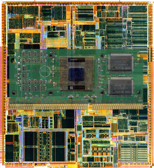
Intel didn't give up on the P6 architecture, but instead waited until 1997 when it released the Pentium II. The Pentium II managed to overcome nearly all of the negative aspects of the Pentium Pro. Its underlying architecture was similar to the Pentium Pro, and it continued to use a 14-stage pipeline with several enhancements to the core to improve IPC. The L1 grew to 16KB data + 16KB instruction caches.
Intel also moved to more affordable cache chips attached to a larger silicon package to reduce production costs. This was an effective way of making the Pentium II less expensive, but these memory modules were unable to operate at the CPU's full speed. Instead, the L2 cache ran at half-frequency, and on these early processors that was sufficient to increase performance.
Get Tom's Hardware's best news and in-depth reviews, straight to your inbox.
Intel also added support for the MMX instruction set. The CPU cores used inside of the Pentium II, code-named "Klamath" and "Deschutes," were also sold as Xeon and Pentium II Overdrive products for servers. The highest-performance models contained 512KB of L2 cache and ran at 450 MHz.
P6: Pentium III And The Race To 1 GHz
Intel planned to follow up the Pentium II with a processor based on its Netburst architecture, but it wasn't quite ready. Instead, Intel pushed the P6 architecture out again as the Pentium III.
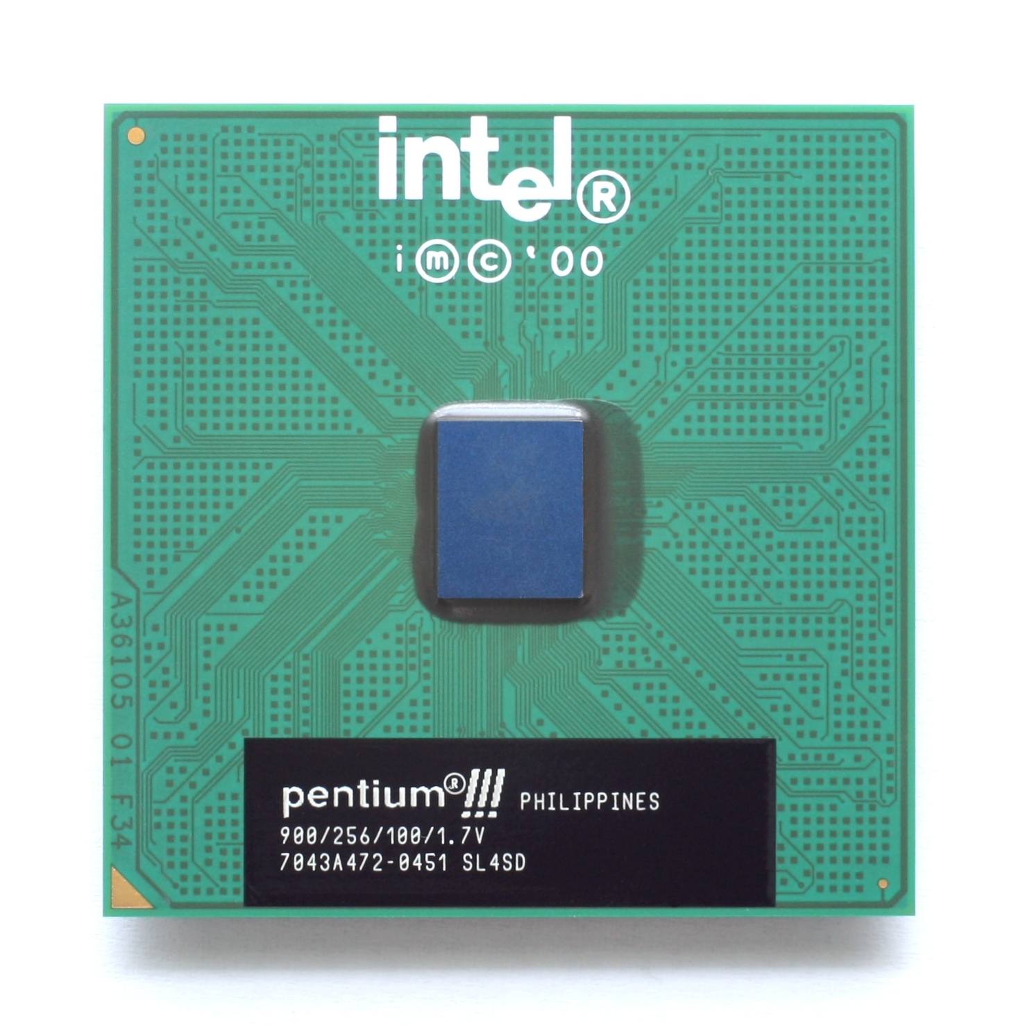
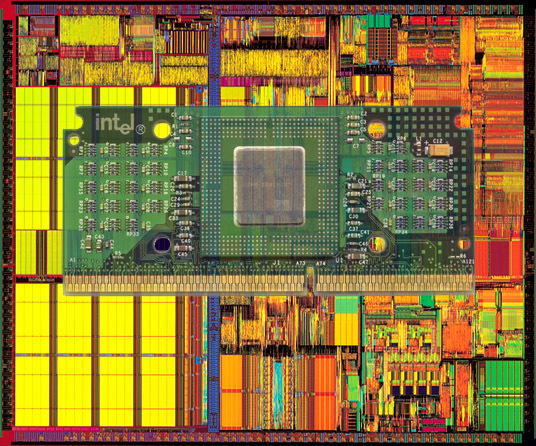
The first of these processors, code-named "Katmai," was rather similar to the Pentium II in that it used a slotted cartridge containing lower-quality L2 cache at half of the CPU's speed. The underlying architecture incorporated other significant changes, as several parts of the 14-stage pipeline were fused together, shortening it to 10 stages. Thanks to the updated pipeline and an increase in clock speed, the first of the Pentium III processors typically outperformed their Pentium II counterparts by a small margin.
Katmai was produced using 250nm transistors. However, following the move to a 180nm fabrication process, Intel was able to boost the Pentium III's performance significantly. This updated implementation, code-named "Coppermine," moved the L2 cache into the CPU and reduced its capacity by half (down to 256KB). But because it was able to run at the processor's frequency, performance still shot up.
Coppermine was Intel's competitor to AMD's Athlon in the race to break 1 GHz, which it succeeded in doing. Intel attempted to produce a 1.13 GHz model, but it was ultimately recalled after investigation from Dr. Tom Pabst of Tom's Hardware discovered that it was unstable. This left the 1 GHz model the fastest Coppermine-based Pentium III.
The last of Pentium III cores was named "Tualatin." It moved to a 130nm process that facilitated clock rates as high as 1.4GHz. It also increased the L2 cache back to 512KB, which helped improve performance somewhat.
P5 And P6: Celeron And Xeon
Around the release of the Pentium II, Intel also introduced its Celeron and Xeon product lines. These products used the same core as the Pentium II or Pentium III, but with varying amounts of cache. The first Celeron-branded processors based on the Pentium II had no L2 cache at all, which resulted in horrible performance. Later models based on the Pentium III had half of the L2 cache disabled compared to their Pentium III counterparts. This resulted in Celeron processors that used the Coppermine core containing just 128KB of L2 cache; later models based on Tualatin increased this to 256KB.
These half-cache derivatives became known as the Coppermine-128 and the Tualatin-256. Intel sold them at clock speeds comparable to the Pentium III, which allowed them to perform well and made them highly competitive against AMD's Duron processors. Microsoft used one of the Coppermine-128 Celeron processors clocked at 733 MHz as the CPU inside of its Xbox gaming console.
The first Xeon processors were similar, but they contained more L2 cache. The Pentium II-based Xeon processors contained at least 512KB, the same as Pentium II CPUs, whereas higher-end models could have up to 2MB.
MORE: Best CPUs
MORE: Best CPU Cooling
MORE: Intel & AMD Processor Hierarchy
MORE: All CPU Content
Netburst: Introduction
Before discussing Intel's Netburst architecture and the Pentium 4, it is important to examine the idea behind its deep pipeline, which describes the process whereby instructions move through a core. Pipeline stages often perform multiple tasks, but sometimes they're devoted to single functions. By either adding new hardware or splitting one stage into multiple stages, the execution pipeline can be extended. The processor pipeline can also be shrunk by removing hardware or by combining the components in multiple stages down into a single stage.
The length or depth of the pipeline has a direct impact on latency, IPC, clock speed and the architecture's throughput requirements. Longer pipelines typically require higher amounts of bandwidth, but if the pipeline is kept adequately fed with data, then each stage in the pipeline stays busy. Processors that have longer pipelines typically are able to run at higher clock rates as well.
The trade-off is significantly higher latency inside of the processor, as data flowing through it must stop at each stage for a certain number of clock cycles. Processors using a long pipeline tend to have lower IPC as well, which is why they rely on significantly higher frequencies to increase performance. Over the years, processors implementing both philosophies have proven successful. Neither approach is necessarily flawed.
Netburst: Pentium 4 Willamette And Northwood
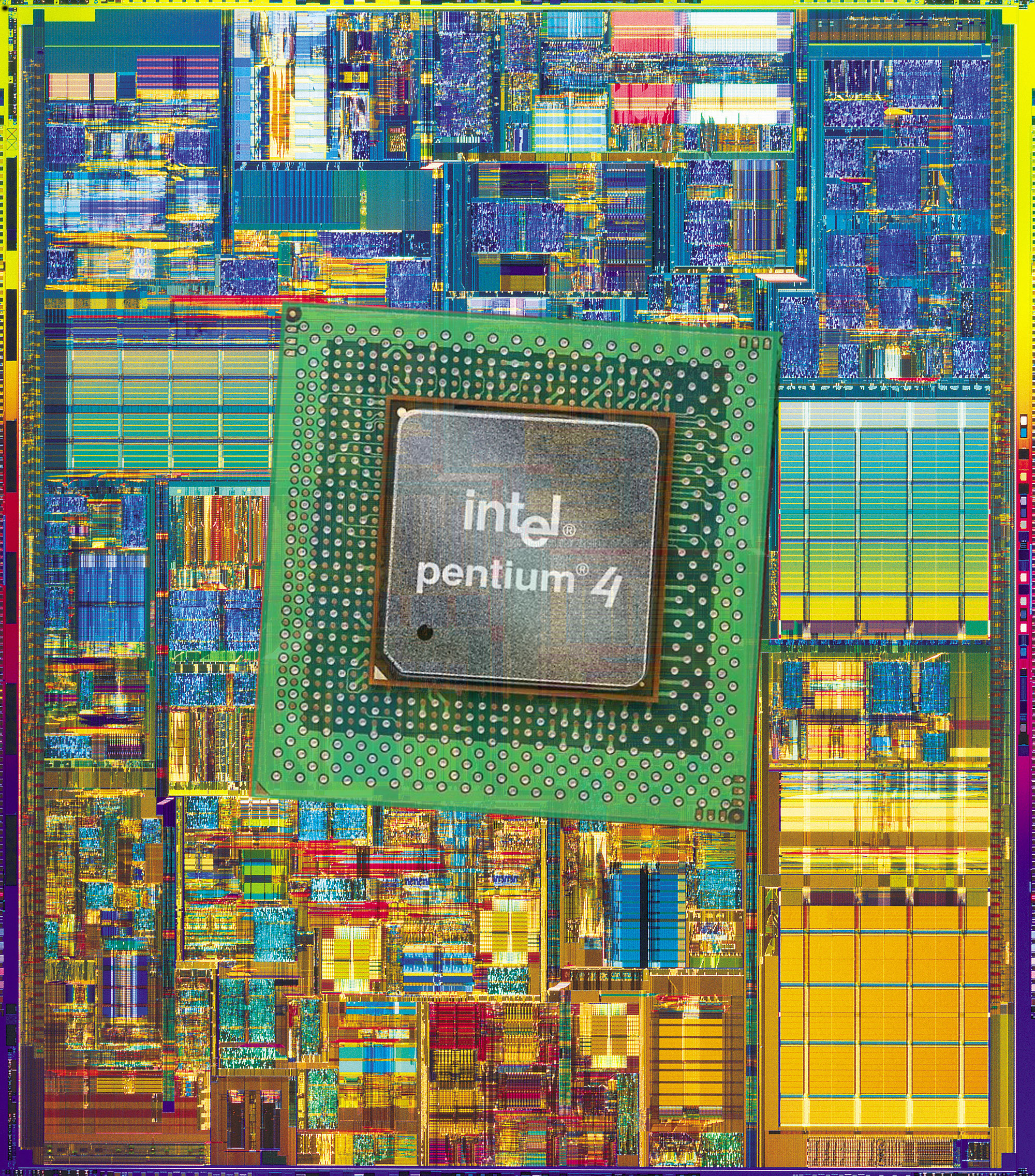
In 2000, Intel's Netburst architecture was finally ready, and it was pushed into production as the Pentium 4. The combination would carry Intel's top-end CPUs for the next six years. The first implementation was named "Willamette," which carried Netburst and the Pentium 4 through the first two years of its life. This was a troubled time for Intel, however, and the chip struggled to outperform the Pentium III. Netburst enabled significantly higher frequencies, and Willamette managed to hit 2 GHz, but the Pentium III at 1.4 GHz was still faster in some tasks. AMD's Athlon processors enjoyed a healthy performance lead during this period.
The problem with Willamette was that Intel stretched the pipeline out to 20 stages and planned to hit even higher clock rates beyond 2 GHz, but due to power consumption and heat issues, it was unable to reach those goals. The situation improved with Intel's 130nm design known as "Northwood," which scaled up to 3.2 GHz and doubled the L2 cache from 256KB to 512KB. Netburst's power consumption and heat issues persisted. However, Northwood nevertheless performed significantly better and was highly competitive against AMD.
On high-end models, Intel also introduced its Hyper-Threading technology to improve resource utilization in environments that emphasized multitasking. Hyper-Threading wasn't as beneficial on Northwood as it is on present-day Core i7 processors, but it did push performance up by a few percentage points.
Willamette and Northwood were released inside of Celeron- and Xeon-branded CPUs as well. As with the previous generation of Celeron- and Xeon-based products, Intel raised or lowered the L2 cache size in order to distinguish their performance.
P6: Pentium-M
As Netburst was designed as a high-performance architecture that was fairly power hungry, it didn't translate well to mobile systems. Instead, in 2003 Intel created its first architecture designed exclusively for notebooks. The Pentium-M was based on the P6 architecture, but with a longer 12-14 stage pipeline. This was also Intel's first variable-length pipeline, which meant that instructions could be executed after moving through just 12 stages if the information required for the instruction was already loaded into cache. If not, it had to go through two additional stages to load the data.
The first of these processors was crafted with 130nm transistors and contained a 1MB L2 cache. It managed to hit 1.8 GHz while consuming just 24.5W of power. A later revision known as "Dothan" was released in 2004 and transitioned to 90nm transistors. This enabled Intel to increase the L2 cache to 2MB and, combined with a number of core enhancements, provide a decent IPC throughput improvement. The CPU also scaled up to 2.27 GHz with a slight increase of power to 27W.
The Pentium-M architecture would eventually be used inside of the Stealey A100 mobile CPUs before being replaced by Intel's line of Atom processors.
Netburst: Prescott
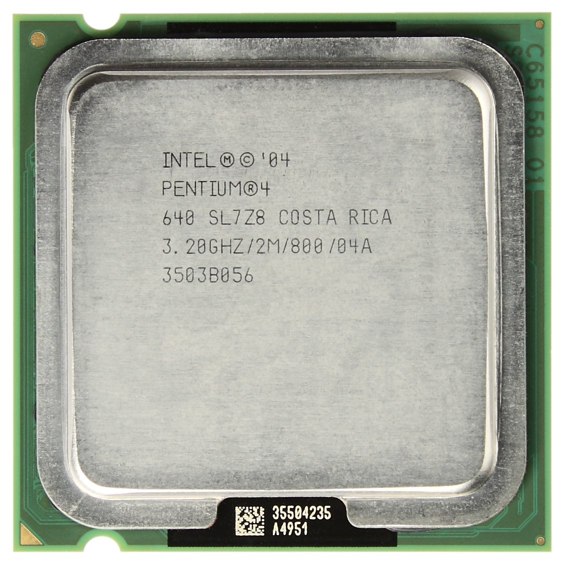
Northwood carried the Netburst architecture from 2002 until 2004, after which Intel launched Prescott with numerous enhancements. It used a 90nm fabrication process that enabled Intel to increase the L2 cache to 1MB. Intel also introduced the new LGA 775 interface that featured support for DDR2 memory and a faster quad-pumped FSB than the first Northwood-based CPUs. These changes resulted in Prescott having significantly more bandwidth than Northwood, which was vital to increasing Netburst's performance. Prescott was also Intel's first 64-bit x86 processor, allowing it to access more RAM and operate on 64 bits at a time.
Prescott was supposed to be the crown jewel in Intel's family of Netburst-based processors, but instead it was a fiasco. Intel again extended its execution pipeline, this time to 31 stages. The company hoped to increase clock rates enough to offset the longer pipe, but it was only able to hit 3.8 GHz. Prescott simply ran too hot and consumed too much power. Intel expected the move to 90nm to alleviate this issue, but the increased transistor density made cooling more difficult. As it was not able to hit higher frequencies, Prescott's evolutionary changes hurt overall performance.
Even with all of the enhancements and extra cache, Prescott was, at best, on par with Northwood at any given clock rate. Around the same time, AMD's K8 processors were also moving to smaller transistors that enabled them to hit higher frequencies. For this brief time period, AMD dominated the desktop CPU market.
Netburst: Pentium D
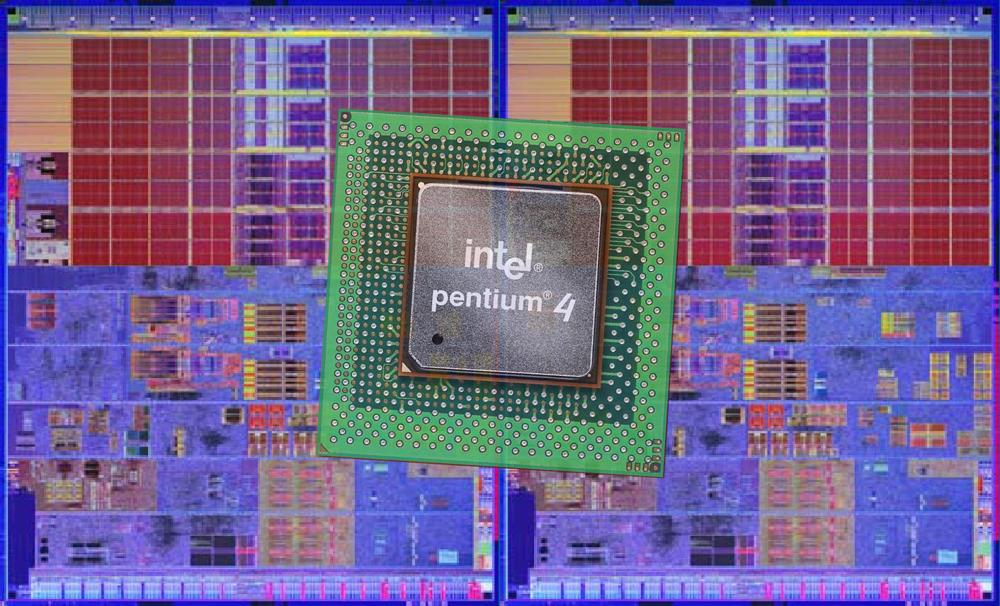
In 2005, the race was on to produce the first consumer-oriented dual-core processor. AMD had already announced its dual-core Athlon 64, but it wasn't available yet. Intel rushed to beat AMD by using a multi-core module (MCM) that contained two Prescott dies. The company christened its dual-core processor the Pentium D, and the first model was code-named "Smithfield."
The Pentium D launched to criticism, however, as it faced the same issues that plagued Prescott. The heat and power of two Netburst-based dies limited clock rates to 3.2 GHz at most. And because the architecture was bandwidth-limited, Smithfield's IPC suffered as throughput was split between two cores. The implementation wasn't particularly elegant either; AMD's dual-core CPU constructed from one die was considered superior.
Smithfield was followed by Presler, which moved to 65nm transistor technology. It contained two Ceder Mill dies on an MCM. This helped reduce the processor's heat and power consumption, and let Intel raise its clock rate to 3.8 GHz.
There are two key steppings of Presler. The first one had a higher 125W TDP, whereas the later model dropped down to 95W. Thanks to the smaller die size, Intel was able to double the L2 cache as well, so each die had 2MB. A few enthusiast models also featured Hyper-Threading, allowing the CPU to address four threads simultaneously.
All Pentium D processors supported 64-bit software and could take advantage of more than 4GB of RAM.
Core: Core 2 Duo
Intel eventually gave up on its Netburst architecture and instead put its support behind the P6 and Pentium-M design. The company realized that P6 was still viable, and capable of being both efficient and providing excellent performance. It reworked the architecture into its Core design. Like the Pentium-M, it used a 12 to 14 stage pipeline that was significantly shorter than Prescott's 31-stage implementation.
Core proved to be highly scalable, and Intel was able to push it into service on mobile systems with TDPs as low as 5W and high-end servers with 130W ceilings. Intel mostly sold it as "Core 2 Duo" or "Core 2 Quad" products, but Core was also used inside of Core Solo-, Celeron-, Pentium- and Xeon-branded CPUs. The dies used were built using two CPU cores, and quad-core designs used two dual-core dies on an MCM. Single-core versions, meanwhile, had one core disabled. L2 cache size ranged from 512KB up to 12MB.
With the improvements made to the Core architecture, Intel could again compete against AMD. The PC market entered a golden age filled with extremely competitive high-performance processors that are still viable to this day.
-
abryant Archived comments are found here: http://www.tomshardware.com/forum/id-3322311/history-intel-cpus.htmlReply -
mitch074 Strange that Itanium is missing, the Celeron 300A/333 is gone, the original Pentium bug disappeared, no mention is made that the 487 was actually a fully active 486DX, and that AMD led the desktop for "a short time" while it led from the moment Netburst came out (2000) to the moment Core replaced it (2006). On another note, a 64-bit CPU doesn't run 64-bit software faster : it is required to have one to run some. But since AMD came up with x86-64, I guess some approximation is allowed...Reply -
Tom Griffin Remember the ABIT BP6a motherboard; I was running dual Celery (Celeron) 300mhz processors overclocked to 533mhz. What a flashback.Reply -
AndrewJacksonZA 1) Where can we see what was updated please?Reply
2) Where are the Phi CPUs please?
3) Where can we view this as a one-pager please? -
ta152h There are quite a few mistakes here.Reply
For one, the 8086 was not available in higher clock speeds than the 8088.
The 8086 could NOT run 8080 code. Source code compatible does not mean that. It means it was very easy to recompile the code so it would work with the newer processor, not that the compiled code would work.
The 286 section is oddly very limited. It was an enormous improvement over the 8086, as it added more memory, much more performance, and also virtual memory and hardware assisted multi-tasking.
The 80386 was not significantly faster than the 286 running 16-bit code, despite what the author says. Clock for clock, they were very close, although 386 based systems tended to get SRAM caches, whereas the 16 and 20 Mhz 286s rarely did.
The 386SX not only cut down the data bus to 16 bits, it also cut down the address bus to 24-bits.
The remarks on the i860 are bizarre. " ... it was nearly impossible to correctly list every instruction from beginning to end when compiling the program. " This is wrong, it was just very difficult to order the instructions very efficiently. Of course it had no problem listing them correctly, or the program wouldn't run. Intel tried it again with Itanium, and depended on the compilers to order instructions very efficiently, and also had difficulties.
The author oddly left out the most significant part of the 486; it was the first pipelined x86 CPU, and that was a large part of the performance improvement.
The Pentium's FPU was not 10x faster than the 486, but it was the biggest improvement. Unless you're comparing a very low clocked 486 to a high clocked Pentium. Clock per clock, it was not nearly 10x faster.
Also MMX instructions were not related to the FPU, but were actually integer based.
The first Pentiums actually ran at 66 MHz, but ran really hot, and they had yield problems, so sold 60 MHz Pentiums along with them, at a significant discount. Most people bought the 60 MHz because they were so much cheaper initially, but 66 MHz was out there.
The Pentium MMX only reached 233 MHz as sold by Intel, not 300 MHz.
The Pentium III (Katmai) was a Pentium II with SSE instructions added, nothing more. The nonsense about fewer pipelines and IPC improvements (outside of SSE code) is fabricated with regards to Katmai.
The Celeron originally had no cache, but there was another version (not a Coppermine based) that had 128K cache on the processor. In some ways, it was faster than the Pentium III it was based on, because the cache was faster.
Coppermine's cache was wider, and generally superior, but Celeron's were very competitive with Katmai based products, and were the favorites of overclockers. -
mitch074 Reply21307316 said:The Celeron originally had no cache, but there was another version (not a Coppermine based) that had 128K cache on the processor. In some ways, it was faster than the Pentium III it was based on, because the cache was faster..
The Celeron 300A/333 you're referring to is the Mendocino core, wasn't based on Pentium III - it didn't have support for SSE. It can be seen as a precursor for Pentium III inasmuch as it had 128 Kb of level 2 non-inclusive low-latency cache - and it was the first Intel P6-family CPU to have that.
It was soon replaced with the Coppermine core, which was indeed based on the Pentium III core (SSE) as it was a smaller die (smaller engraving) thus much cheaper to produce. -
milkod2001 Still on Haswell 4770k. Don't see any reasons to upgrade apart from m.2 SSDs maybe but have regular SATA SSD and there might be no difference in actual performance. Right?Reply
