The Core i7-4770K Review: Haswell Is Faster; Desktop Enthusiasts Yawn
Intel's Haswell architecture is finally available in the flagship Core i7-4770K processor. Designed to drop into an LGA 1150 interface, does this new quad-core CPU warrant a complete platform replacement, or is your older Sandy Bridge-E system better?
Haswell Turns Into Intel's Fourth-Gen Core Architecture
Editor’s Note: Eager to show off what it's doing with Intel’s Haswell architecture, system builder CyberPower PC is offering the Tom’s Hardware audience an opportunity to win a new system based on Intel’s Core i7-4770K processor. Read through our review, and then check out the last page for more information on the system, plus a link to enter our giveaway!
Do you know what it’s like to be at the top of your game, the nearest competitor several strides behind? Well, maybe not. But Intel sure does. When it comes to desktop CPUs, the company’s top-end parts continue to stave off AMD's best efforts. That applies to raw performance and efficiency.
We love fast, and we love efficient. But we also like to see healthy competition driving innovation. And again, on the desktop, there’s not enough of that to push Intel. Ivy Bridge-based CPUs are generally a small step up from the generation prior. And although the Sandy Bridge architecture included a number of notable improvements, unprecedented integration gave away Intel’s growing focus on mobility. Even as we got our hands on great features like Quick Sync, Intel was chiseling away at its enthusiast equity by limiting overclocking to K-series SKUs.
Article continues belowExpect more of the same from Haswell. You're going to see notable per-clock performance improvements, faster graphics, and additional features able to accelerate specific workloads. But you’re also going to witness a clumsy handling of overclocking (again), some strange decisions on the graphics side (again), and incremental gains that’ll have some of us upgrading our desktops, but more folks looking for Haswell-powered mobile platforms.
That's entirely by design, by the way. An emphasis on power is front and center with Haswell. And as a result, this architecture is going to span the broadest range of devices Intel has ever touched with one design. But I’ll argue that enthusiasts on the desktop take a back seat to make it all possible.
Meet Haswell, Now Known As Intel’s Fourth-Gen Core Architecture
Intel is rolling out the details of its Haswell-based processors in a staggered launch. The company plans to ship multiple variations of the architecture across a number of different interfaces, from very low-power segments to very performance-sensitive ones. However, the only arrangement emerging today is the quad-core SoC. Technically, Intel is talking desktop and mobile, though we’re deliberately focusing on the Core i7-4770K desktop CPU. I published a preview of Core i7-4770K’s performance almost three months ago, and that story has some information about Intel’s plans as well.
Get Tom's Hardware's best news and in-depth reviews, straight to your inbox.
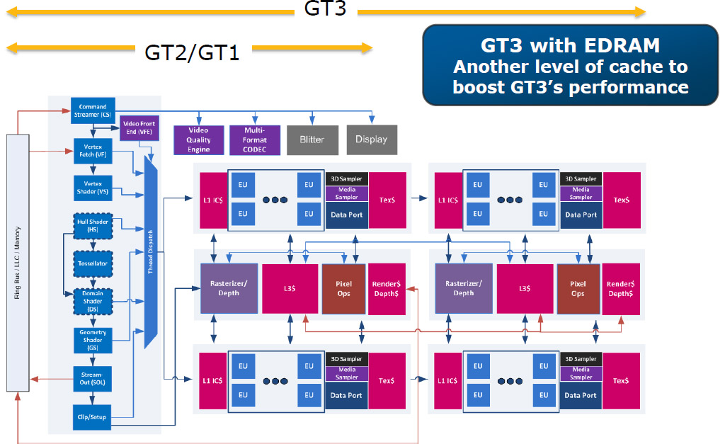
Haswell-based quad-core processors will ship in two configurations to cover the mobile and desktop markets. Only one is ready today, though. That chip features the HD Graphics 4600 engine, also known as GT2. The second, with Iris Pro Graphics 5200 (or GT3e) is coming later. Intel's engineers claim that Iris Pro scales incredibly well given a lofty power ceiling and enough cooling. However, CPUs endowed with the higher-end graphics engine are BGA-only, meaning they’re soldered down. So, enthusiasts buying LGA 1150-equipped motherboards will only find Core i7 and Core i5 CPUs with four cores and HD Graphics 4600 (technically, there’s also a 35 W Core i5 with fewer cores, but it’s still under wraps).
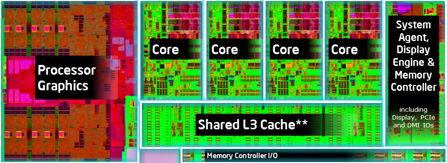
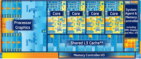
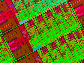
This implementation of Haswell is composed of 1.6 billion transistors, up from a comparable Ivy Bridge configuration’s 1.4 billion. Optimized expressly for Intel’s 22 nm node, the die measures 177 square millimeters, just slightly larger than quad-core Ivy Bridge at 160 mm².
Put Ivy Bridge and Haswell right next to each other and you might have a difficult time telling them apart. After all, there’s “only” a 200 million-transistor delta separating the two. That 14% growth in transistor count largely comes from a 25% increase in graphics resources compared to last generation.
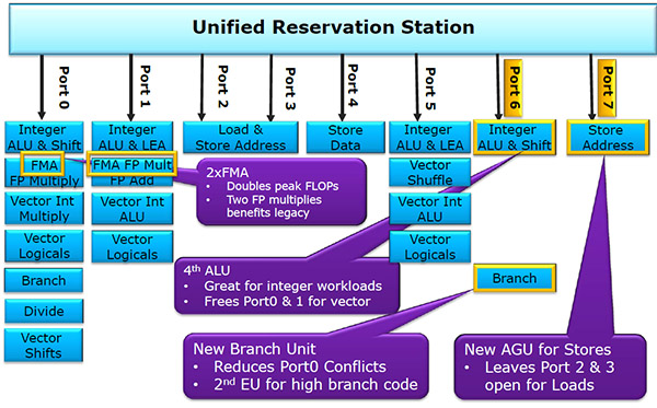
That’s not to say the processor cores go untouched. Intel says it put specific emphasis on speeding up both today’s legacy code as well as applications we’ll see in the future. To that end, larger buffers enlarge the out-of-order window, which means instructions that would have previously waited for execution can be located and processed sooner. Haswell’s window is 192 instructions. Sandy Bridge was 168. Nehalem was 128. The Haswell branch predictor is improved, too. This is something Intel manages to do every generation—and for good reason, since it simultaneously enables better performance and prevents the wasted work of a branch getting predicted incorrectly. Previously, Intel’s architecture was able to execute six operations per clock cycle. However, Haswell gets two additional ports (one integer ALU and one store), enabling up to eight operations per cycle. And workloads with large data sets should see a benefit from a larger L2 TLB.
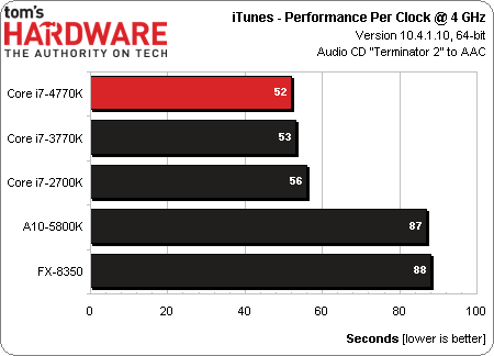
All of those changes add up to significant improvement in Haswell’s IPC compared to Ivy Bridge. That’s where we expect most of the speed-up in general-purpose apps to come from this generation, since the top-end Core i7-4770K runs at the same 3.5 GHz as -3770K.
Sure enough, when we set five different processors (employing four different architectures) to the same constant 4 GHz, we see, first, how much more work Intel gets done compared to AMD and, second, a steady progression forward in Intel’s performance.
In addition to the two execution ports Intel adds to Haswell, ports one and two now feature 256-bit Fused Multiply-Add units, doubling the number of peak theoretical floating-point operations per cycle. Integer math gets a big boost as well from AVX2 instruction support.
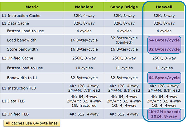
Of course, multiplying the architecture’s compute potential means little if you can’t get data into the core fast enough. So, Intel also made a number of changes to its caches. Haswell’s L1 and L2 caches are the same size as they were in Ivy Bridge (there’s a 32 KB L1 data, 32 KB L1 instruction, and 256 KB L2 cache per core). Bandwidth to the caches is up to doubled, though, and we’ll see in our synthetic testing that the L1D is indeed quite a bit faster. Intel claims that it can do one read every cycle from the L2 (versus one read every other cycle in Ivy Bridge), but we aren’t able to replicate those figures in our own testing.
| Header Cell - Column 0 | Cores / Threads | Base Freq. | Max. Turbo | L3 | HD Graphics | Graphics Max Freq. | TDP | Price |
|---|---|---|---|---|---|---|---|---|
| Fourth-Gen Core i7 Family | ||||||||
| 4770T | 4/8 | 2.5 GHz | 3.7 GHz | 8 MB | 4600 | 1,200 MHz | 45 W | $303 |
| 4770S | 4/8 | 3.1 GHz | 3.9 GHz | 8 MB | 4600 | 1,200 MHz | 65 W | $303 |
| 4770 | 4/8 | 3.4 GHz | 3.9 GHz | 8 MB | 4600 | 1,200 MHz | 84 W | $303 |
| 4770K | 4/8 | 3.5 GHz | 3.9 GHz | 8 MB | 4600 | 1,250 MHz | 84 W | $339 |
| 4770R | 4/8 | 3.2 GHz | 3.9 GHz | 6 MB | Iris Pro 5200 | 1,300 MHz | 65 W | N/A |
| 4765T | 4/8 | 2.0 GHz | 3.0 GHz | 8 MB | 4600 | 1,200 MHz | 35 W | $303 |
| Fourth-Gen Core i5 Family | ||||||||
| 4670T | 4/4 | 2.3 GHz | 3.3 GHz | 6 MB | 4600 | 1,200 MHz | 45 W | $213 |
| 4670S | 4/4 | 3.1 GHz | 3.8 GHz | 6 MB | 4600 | 1,200 MHz | 65 W | $213 |
| 4670K | 4/4 | 3.4 GHz | 3.8 GHz | 6 MB | 4600 | 1,200 MHz | 84 W | $242 |
| 4670 | 4/4 | 3.4 GHz | 3.8 GHz | 6 MB | 4600 | 1,200 MHz | 84 W | $213 |
| 4570 | 4/4 | 3.2 GHz | 3.6 GHz | 6 MB | 4600 | 1,150 MHz | 84 W | $192 |
| 4570S | 4/4 | 2.9 GHz | 3.6 GHz | 6 MB | 4600 | 1,150 MHz | 65 W | $192 |
The Core i7-4770K gives us an 8 MB shared L3 cache, similar to Core i7s before it. Although the Sandy and Ivy Bridge designs employed a single clock domain that kept the cores and L3 running at the same speed, Haswell decouples them. Our cache bandwidth benchmark reveals a slight hit to L3 throughput, though improvements elsewhere in the System Agent keep the results fairly even.
Haswell offers the same 16 lanes of PCI Express 3.0 connectivity as Ivy Bridge, and validated memory data rates up to 1,600 MT/s. The desktop line-up’s thermal targets are quite a bit different as a result of Intel’s fully-integrated voltage regulator, but an upper bound of 84 W isn’t extreme by any stretch and a floor of 35 W is pretty familiar.
All of Intel’s upgradable processors now drop into an LGA 1150 interface, meaning any decision to adopt Haswell is also going to require a motherboard purchase, at least. So, before you drop several hundred dollars on a brand new platform, let’s figure out if Core i7-4770K is worth the investment.
Current page: Haswell Turns Into Intel's Fourth-Gen Core Architecture
Next Page HD Graphics 4600: 3D And Quick Sync-
Danny N Biggest question is if its worth upgrading my cpu i5 750 4.0ghz to Haswell or my gfx card ati 5870 to nvidia 7xx, my main pc use is for Maya, After FX and some fps gaming. Any input would be appriciated cause I'm leaning towards a cpu upgrade atm.Reply -
refillable @Danny NReply
You shouldn't ask here. Perhaps you should get an i7-4770k and a 7970(?) I heard that kepler cards does not perform that good in Maya and Aftereffects (In OpenCL). -
envy14tpe Seriously. What did people expect? Of course it's better but nothing out of the ordinary for Intel.Reply -
enewmen For me it's not about the 10% gain over SB. It's more like a huge gain over a C2Q, floating point performance over SB (should matter later), and lower watts. I hope THG can expand the Power Consumption and Media Encoding later - check the Watts idle more and fast quick-sync media encoding quality loss. My 2 cents..Reply
EDIT:
other sites have reported much lower watts idle, so a lot doesn't make sense or the 4770k has a very slow throttle.
http://hexus.net/tech/reviews/cpu/56005-intel-core-i7-4770k-22nm-haswell/?page=15
http://www.techspot.com/review/679-intel-haswell-core-i7-4770k/page13.html
