At The Last Second: AMD's Trump Card - The Athlon XP 2600+
And Now, More Speed: Copper Interconnects At Nine Levels
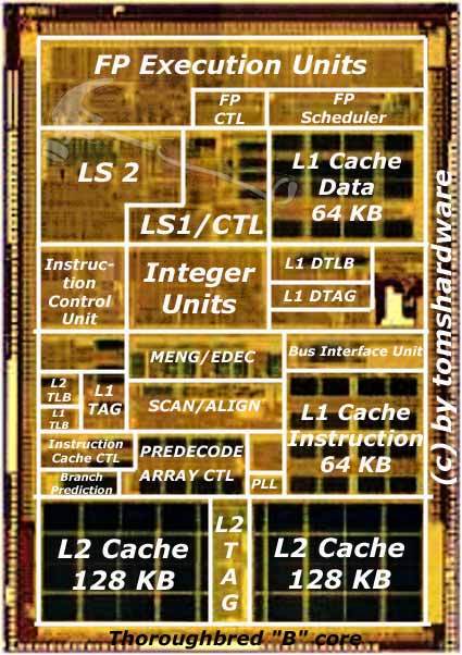
Architecture of the new Thoroughbred "B" core.
A modern CPU, such as the AMD Athlon XP or the Intel Pentium 4, consists of a transistor layer (silicon) and multiple layers of interconnects. Ever since the launch of the first Athlon with the Thunderbird core with its six layers of interconnects, AMD has been increasing the number of layers. The Palomino core followed with seven layers of interconnects, which were required for the SSE logic as well as for the optimization of the cache lines.
The next step came with the Thoroughbred "A," which added another layer. By shortening the circuit paths and distances by 0.05 micron to 0.13 micron, as well as re-organizing all of the components, additional new circuits were necessary. The current record-holder is the Thoroughbred "B" with a total of nine interconnect layers made of copper.
The increased number of circuit paths results in better conductivity for the connections within the processor, which, in turn, automatically decreases the amount of thermal loss. Also, AMD has added further condensers in order to significantly decrease the interference of transistors at high clock speeds in this combination of interconnect layers and capacities.
View of the interconnect layers in a modern processor. Pictured here is the P4 Northwood.
To sum up: the resistances between the transistors are increased (crosstalk). To differentiate between the two Thoroughbred types, AMD's new CPU with nine layers was given the designation "B." In the future, AMD plans to use the SOI technique (nearly pure copper interconnects) for the first time with its Barton core. CPUs produced with SOI technology are supposed to process signals faster and with less power consumption. This enables a 35% increase in clock speed with the same power consumption.
Get Tom's Hardware's best news and in-depth reviews, straight to your inbox.
Current page: And Now, More Speed: Copper Interconnects At Nine Levels
Prev Page Power With The Athlon XP 3400+ And 2666 MHz Next Page Heat Dissipation And Clock Increase
