GeForce GTS 250: Nvidia's G92 Strikes Again
The GeForce GTS 250 In Detail
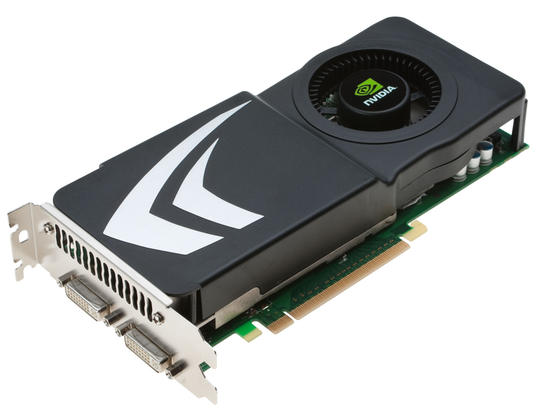
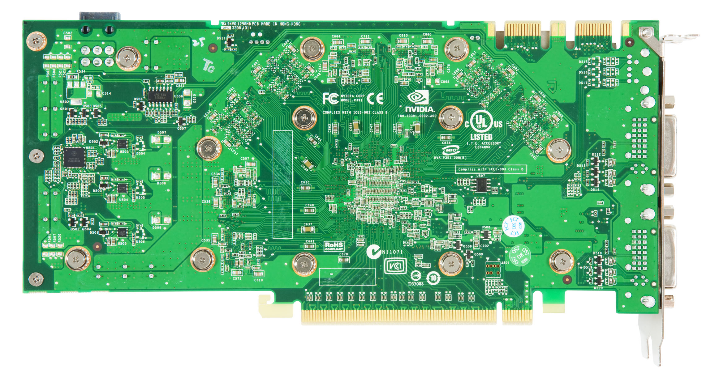
BFG Shows Off Its GeForce GTS 250
As mentioned, the GTS 250 is a GeForce 9800+ by another name. Thus, its specifications should be easy to remember for anyone already familiar with Nvidia’s lineup.
Manufactured on TSMC’s 55 nm process, the card’s G92 GPU sports 754 million transistors and occupies 230 square millimeters of die space—less than half the size of the GT200. It features 128 unified shader processors, 64 texture units, and 16 ROPs.
Whereas most GeForce GTX 9800+ cards came with 512 MB of GDDR3 memory, reference GeForce GTS 250s will instead include 1 GB of GDDR3, according to sources at BFG and Zotac. Both the older and new G92-based boards employ a 256-bit memory bus, though.
A reference GTS 250 employs a 738 MHz core clock, 1,836 MHz shader clock, and 1.1 GHz (2.2 GHz effective) memory clock. But BFG sent us a sample of its GeForce GTS 250 OC Edition with a faster 750 MHz core and 1.12 GHz memory clock, while the shader clock remained unchanged.
| Header Cell - Column 0 | GeForce GTX 260 Core 216 | GeForce GTS 250 | GeForce GTX 9800+ | Radeon HD 4870 | Radeon HD 4850 | Radeon HD 4830 |
|---|---|---|---|---|---|---|
| Manufacturing Process | 55 nm TSMC | 55 nm TSMC | 55 nm TSMC | 55 nm TSMC | 55 nm TSMC | 55 nm TSMC |
| SPs | 216 | 128 | 128 | 800 | 800 | 640 |
| Core Clock | 576 MHz | 738 MHz | 738 MHz | 750 MHz | 625 MHz | 575 MHz |
| Shader Clock | 1,242 MHz | 1,836 MHz | 1,836 MHz | 750 MHz | 625 MHz | 575 MHz |
| Memory Clock | 999 MHz GDDR3 | 1,100 MHz GDDR3 | 1,100 MHz GDDR3 | 900 MHz GDDR5 | 993 MHz GDDR3 | 900 MHz GDDR3 |
| Frame Buffer | 896 MB | 1 GB | 512 MB | 512 MB | 512 MB | 512 MB |
| Memory Bus Width | 448-bit | 256-bit | 256-bit | 256-bit | 256-bit | 256-bit |
| ROPs | 28 | 16 | 16 | 16 | 16 | 16 |
| Price | $229 | est. $149 | $144 | $164 | $139 | $89 |
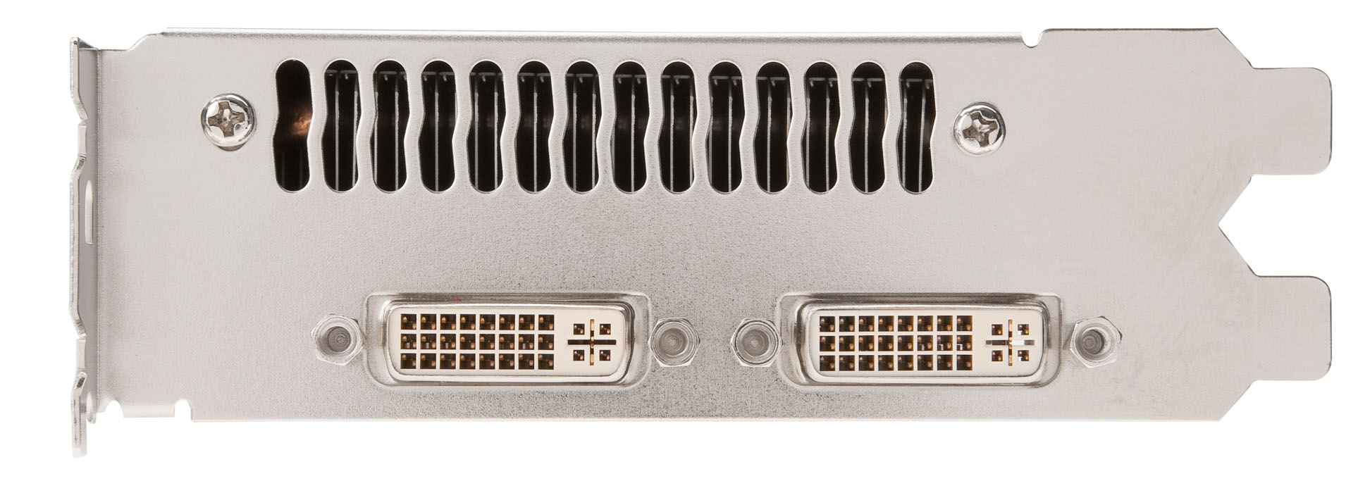
BFG’s card sports two dual-link DVI outputs. And while it supports HDMI output, enabling that feature requires an adapter and audio cable sold separately. It also supports two- and 3-way SLI out of the box; the requisite cables would be included with your SLI-capable motherboard.
Is This A Big Deal?
Get Tom's Hardware's best news and in-depth reviews, straight to your inbox.
At this point, we can’t think of a graphics architecture that has been so re-used. But is that necessarily a bad thing, or a problem, for that matter?
Technologically, it isn’t an issue at all. None of Nvidia’s cards support DirectX 10.1, so it’s not like sticking to an older design has an adverse effect on what the GeForce GTS 250 can do versus its GT200-based big brothers. In fact, so long as performance goes up or sideways as price goes down, we don’t see an issue with the reintroduction of proven technology. Moreover, with software support for CUDA, PhysX, and 3D Vision enabled all the way down to GeForce 8-series GPUs (and PureVideo HD supported by everything down to 9-series GPUs), we see no reason to avoid the GTS 250 simply because it’s a rehash of the GeForce GTX 9800+.
The question changes when you look at it from a marketing angle, though. Officially, Nvidia is updating nomenclature to reflect the way its high-end cards (the GTX 260, 280, 285, and 295) are referenced. The GeForce GTS 250 is thus understood to be a more mainstream entry into that same lineup.
If you’re more cynical, it wouldn’t be a stretch to say that launching the GTS 250 makes it appear (to the less-informed) Nvidia has been up to something in the mid-range market other than selling former flagships at reduced prices.
Indeed, while a new name for the same tech does open a door for confusion amongst mainstream customers, it’s worth noting that the GeForce GTX 9800+ is being end-of-life’d and should cease to be a redundancy in the company’s lineup soon enough.
Current page: The GeForce GTS 250 In Detail
Prev Page The State Of Graphics Next Page Test Setup, Benchmarks, And Notes-
thepinkpanther when the GTX4xx series i guess nvidia will launch the g92 refresh yet again, this time as an entry level graphics card.Reply -
xx12amanxx Hmm no mention of the slower model's Nvidia is going to push instead of these cherry picked Oced model's.I heard these Oced model's were just for reviewers and that most of these cards will actually be slower model's with even less performance.Reply -
johnbilicki "so long as performance goes up or sideways as price goes down, we don’t see an issue with the reintroduction of proven technology"Reply
...which (in the context it has been applied) is the same as saying we don't mind nVidia renaming an 8800GT to a 9800GT and then a 9800GT to a whatever 2xx series...and so on and so forth. My point is simple: nVidia is pulling an extremely sleazy marketing scheme on consumers by renaming existing models. If you goof admit it and get on with life; that's why I appreciated the fact that when the first generation of Phenoms were botched AMD gracefully renamed unaffected quads with a 50 (IE 9650 instead of 9600). Trying to remember all the different names of the exact same model is like dealing with someone who IM's you from five different screen names, eventually you just end up blocking them out. -
cangelini xx12amanxxHmm no mention of the slower model's Nvidia is going to push instead of these cherry picked Oced model's.I heard these Oced model's were just for reviewers and that most of these cards will actually be slower model's with even less performance.Reply
Cherry picked? It's a retail product. -
curnel_D Chris, it's a decent article, but why in the world would you use 512mb models in everyting aside from the 250 and 260. If you would have shown the 1gb 4870, along with a 1gb 9800+, it would have showed a clearer picture of how the 250 is identical to the 9800+/9800/8800GT.Reply
Meh.
And there are MASSIVE rumours saying that Nvidia is hand-picking the review models sent to reviewers, even confirmed by HardOCP. Addressing that in this article would have been great. -
If I'm not mistaken didn't the 9 series and the HD4XXX series launch at about the same time effectively putting them into the same class? So why does everyone love to compare the 2XX series to the 4XXX cards and on top of that usually giving the ram advantage to nvidia i.e. comparing 1GB cards to 512MB cards?Reply
-
sohei i think Nvidia want's to marry this card with us ...love with force is not possible ...we need a new "woman" from nvidia not other clothes ...Nvidia has enough experience with clothes ...they should enter in fashion business like MicrosoftReply -
vaskodogama huh, anyway, I don't like the naming of GT200 cards anyway! AMD's got better price, and naming scheme!Reply
thepinkpantherwhen the GTX4xx series i guess nvidia will launch the g92 refresh yet again, this time as an entry level graphics card.I Agree!


