Why you can trust Tom's Hardware
Intel Adaptive Boost Technology (ABT)
Below is the full list of both the Rocket Lake and Comet Lake Refresh SKUs, and their accompanying boost frequencies. Here's a guide to the different boost technologies that come with the Rocket Lake processors:
- Turbo Boost 2.0: Increased frequency if chip operates below power, current, and temperature specifications.
- Turbo Boost Max 3.0: Fastest cores are identified during binning, then the Windows scheduler targets the fastest two active cores (favored cores) with lightly-threaded applications. Chip must be below power, current, and temperature specifications.
- Single-Core Thermal Velocity Boost: Fastest active favored core can boost higher than Turbo Boost Max 3.0 if below a pre-defined temperature threshold (70C) and all other factors adhere to TB 3.0 conditions.
- All-Core Thermal Velocity Boost: Increases all-core frequency when all cores are active and the chip is under 70C.
- Adaptive Boost Technology: Allows dynamic adjustment of all-core turbo frequencies when four or more cores are active. This feature doesn't have a guaranteed boost threshold — it will vary based on chip quality, your cooler, and power delivery.
Think of Intel's Adaptive Boost Technology (ABT) much like a dynamic auto-overclocking feature that applies to all-core boosts, but remains within warranty. In a nutshell, ABT allows Core i9 processors to opportunistically boost to higher all-core frequencies based upon available thermal headroom and electrical conditions. ABT is the company's fourth boost tech, but it only offers the new feature on its pricey Core i9 K and KF processors.
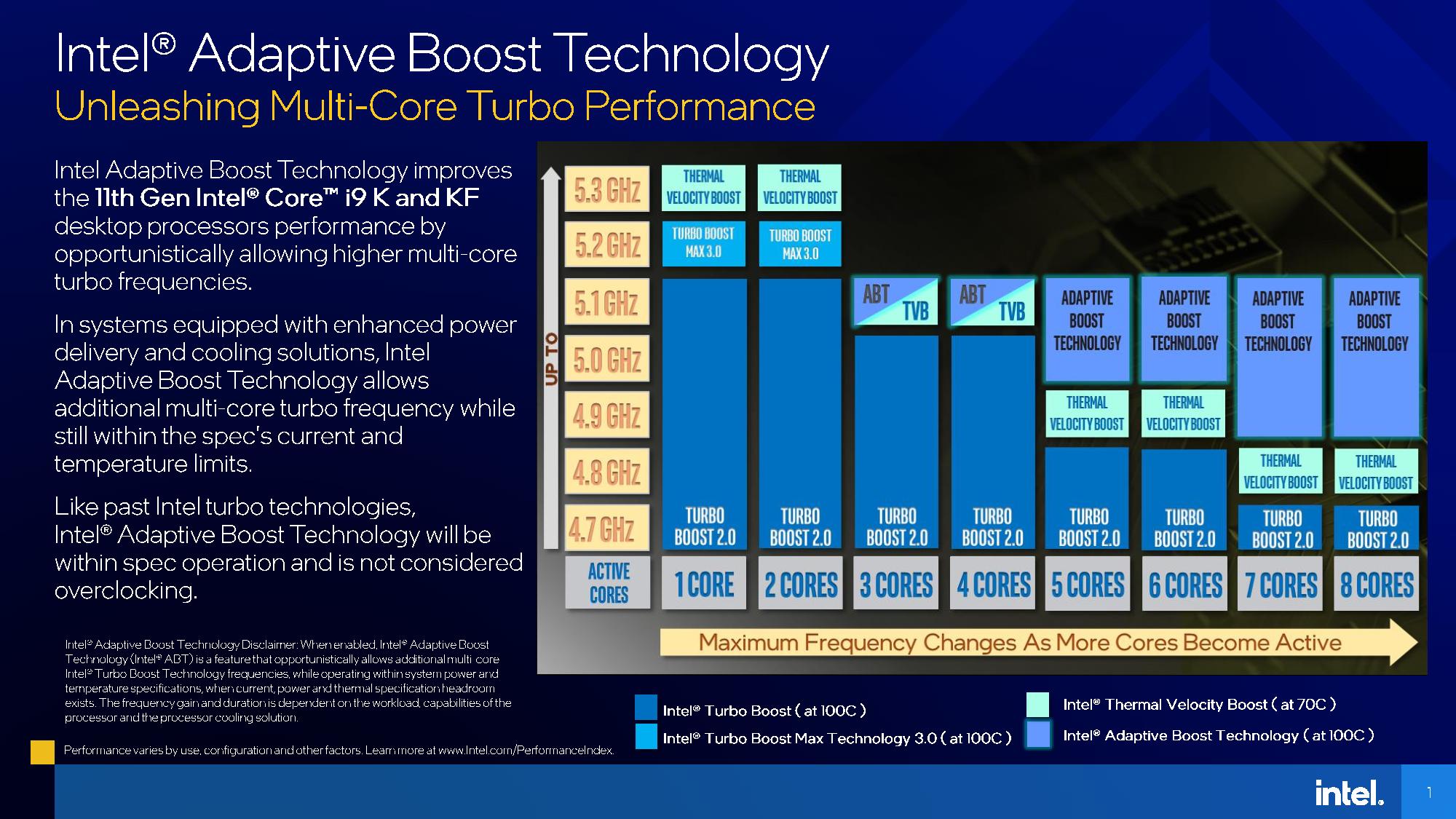
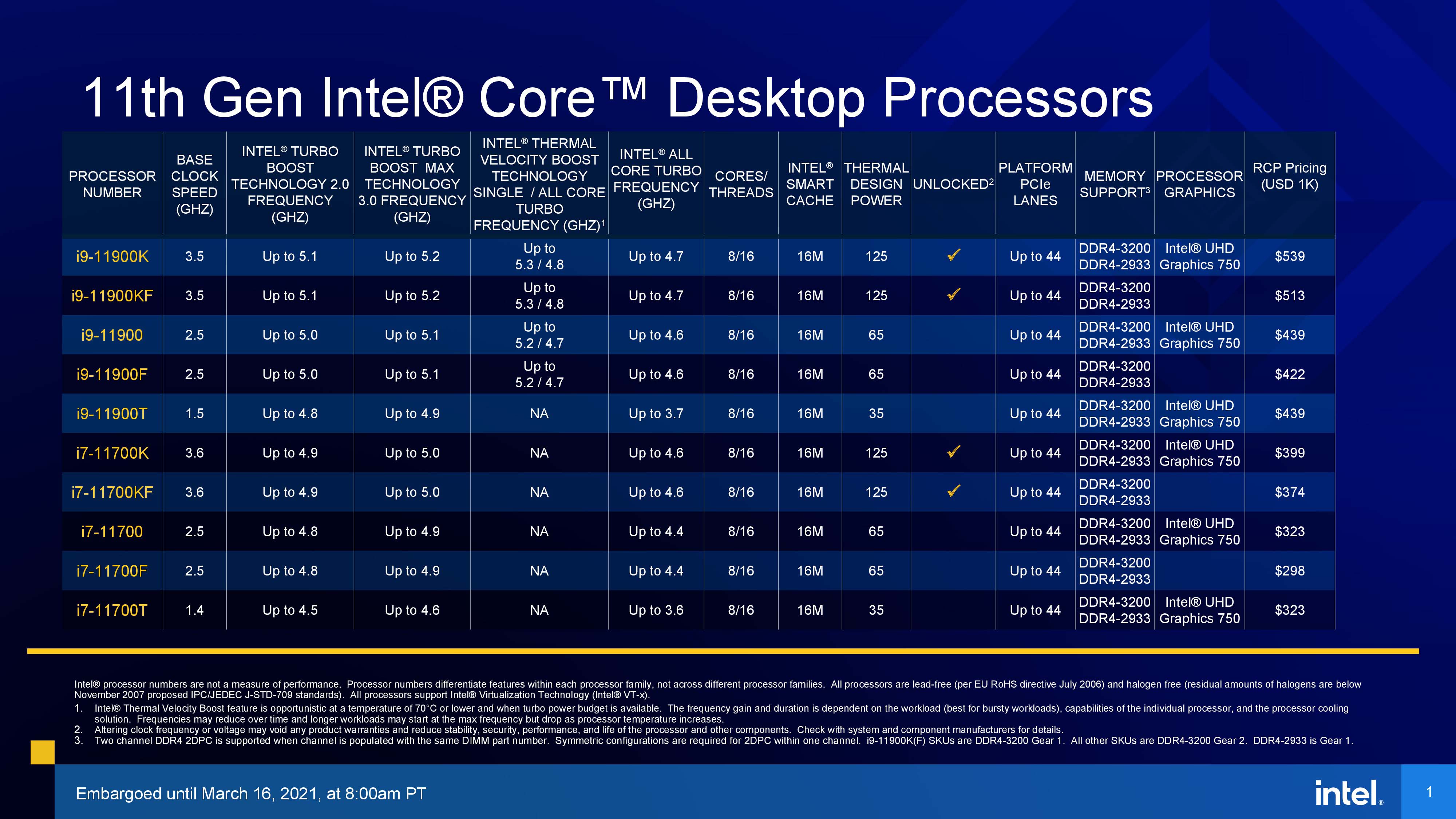
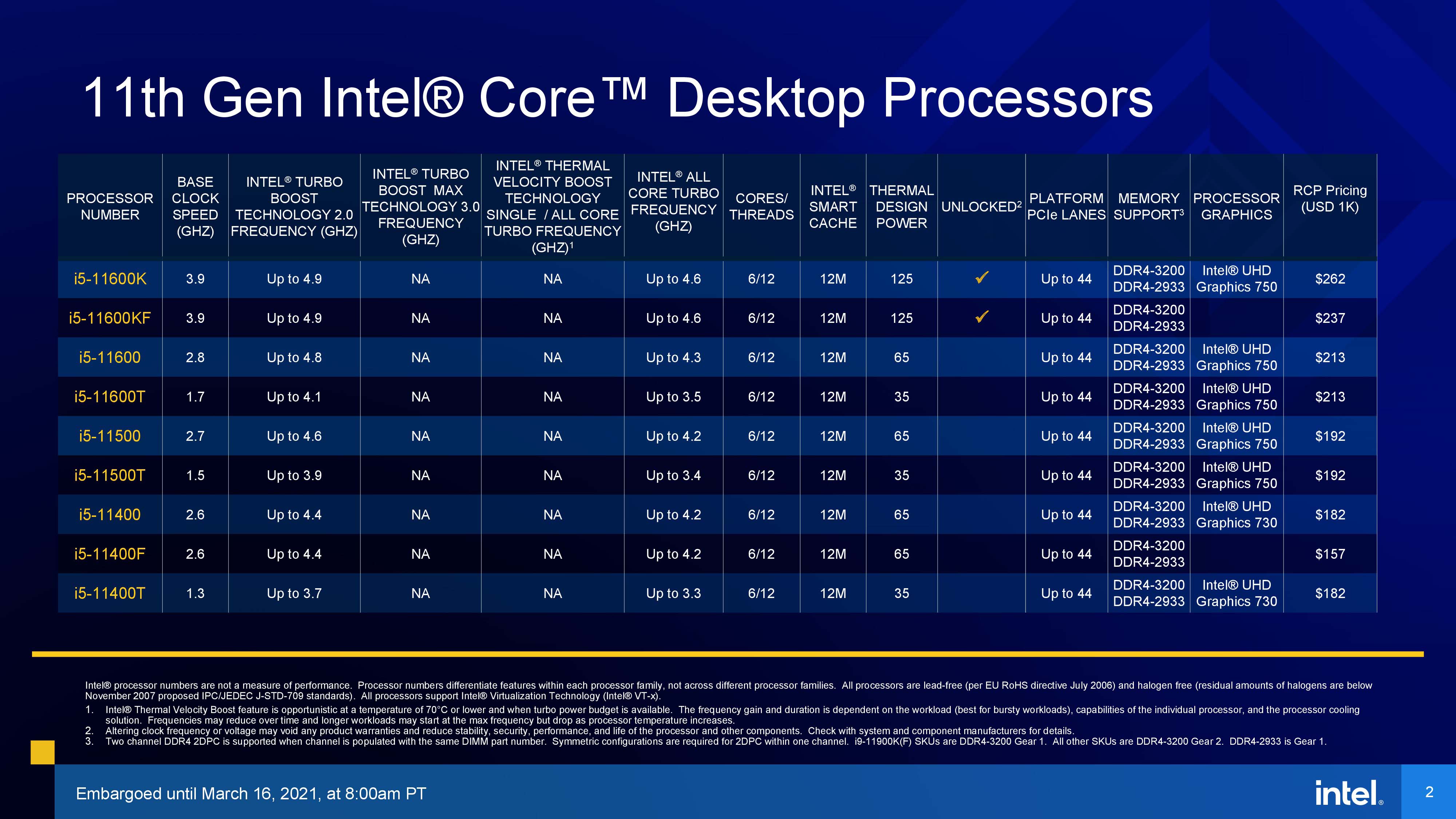
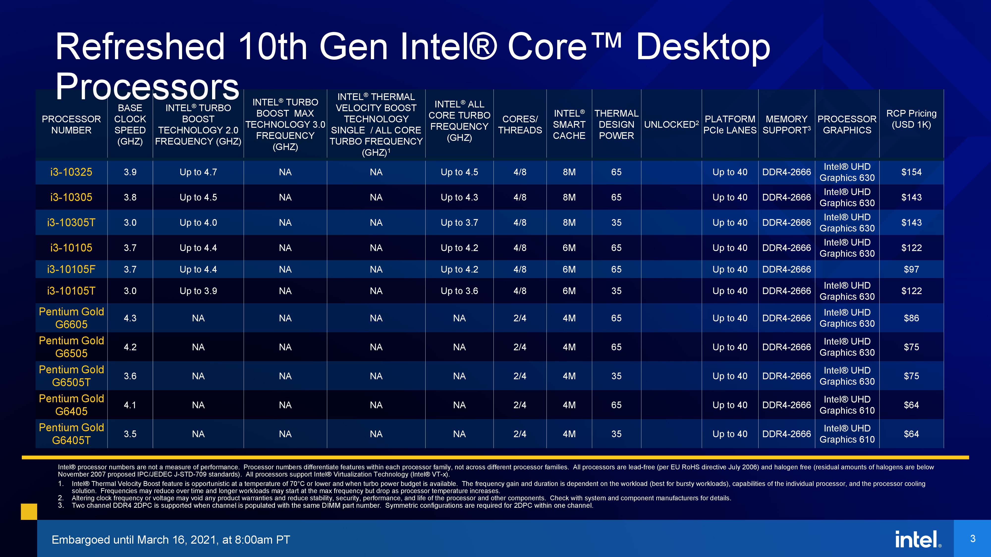
Even though Intel has defined a 5.1 GHz peak for ABT if three or more cores are active, it doesn't come with a guaranteed frequency — peak frequencies will vary based upon the quality of your chip, cooler, and motherboard power delivery. Still, because the chip stays within Intel's spec of a 100C temperature limit and the ICCmax rating, it is a supported feature that doesn't fall into the same classification as overclocking, so it's fully within warranty (it is disabled by default in the motherboard BIOS, however).
In contrast, Intel's other boost technologies boost to pre-defined limits based on the number of active cores, and you're guaranteed that the chip can hit those frequencies if it is below a certain temperature and the motherboard can supply enough power. We have plenty of testing below with Intel's ABT both enabled and disabled.
The Never-Ending 14nm Process Meets New Cypress Cove Microarchitecture
Intel's Skylake architecture debuted on the 14nm process back in 2015, and until today, all of Intel's post-Broadwell mainstream desktop chips have been a derivative of Skylake. These incessant iterations came as a byproduct of Intel's delayed 10nm process and the earlier decision to tightly couple its microarchitectures to specific process nodes, which allowed the company to tune its designs to the capabilities of the silicon. However, this left Intel's architectural advances locked behind the delayed 10nm node.
| Microarchitecture | Year | Process | Max Turbo Clock |
| Broadwell | 2014 | 14nm | 3.8 GHz |
| Skylake | 2015 | 14nm | 4.2 GHz |
| Kaby Lake | 2016 | 14nm+ | 4.5 GHz |
| Coffee Lake | 2017 | 14nm++ | 5.0 GHz |
| Cannon Lake (Kaby Shrink) | 2018 | 10nm | 3.2 GHz |
| Coffee Lake Refresh | 2018 | 14nm++? | 5.0 GHz |
| Comet Lake | 2020 | 14nm++? | 5.3 GHz |
| Sunny Cove (Ice Lake mobile) | 2019 | 10nm (+) | 4.1 GHz |
| Rocket Lake | 2021 | 14nm++? | 5.3 GHz |
| Alder Lake | TBD (2021) | 10nm Enhanced SuperFin | ? |
At its Architecture Day 2018, Intel announced that it would decouple its architectures from specific process nodes, making them portable between nodes so the company could select the best process for each application, and also have a buffer to better absorb any future process node delays. Sunny Cove, which debuted with the 10nm Ice Lake mobile processors, would be the first 'portable' architecture.
Intel cites 10nm's clock speeds, which were initially woefully inadequate at 4.1 GHz, as the primary reason it chose to backport Sunny Cove to create the Cypress Cove architecture present in the Rocket Lake chips. Intel also injected the Xe graphics from 10nm Tiger Lake into the Rocket Lake design to create the UHD Graphics 750 engine (more on that shortly), thus merging two of its newer architectures for the desktop PC.
Get Tom's Hardware's best news and in-depth reviews, straight to your inbox.
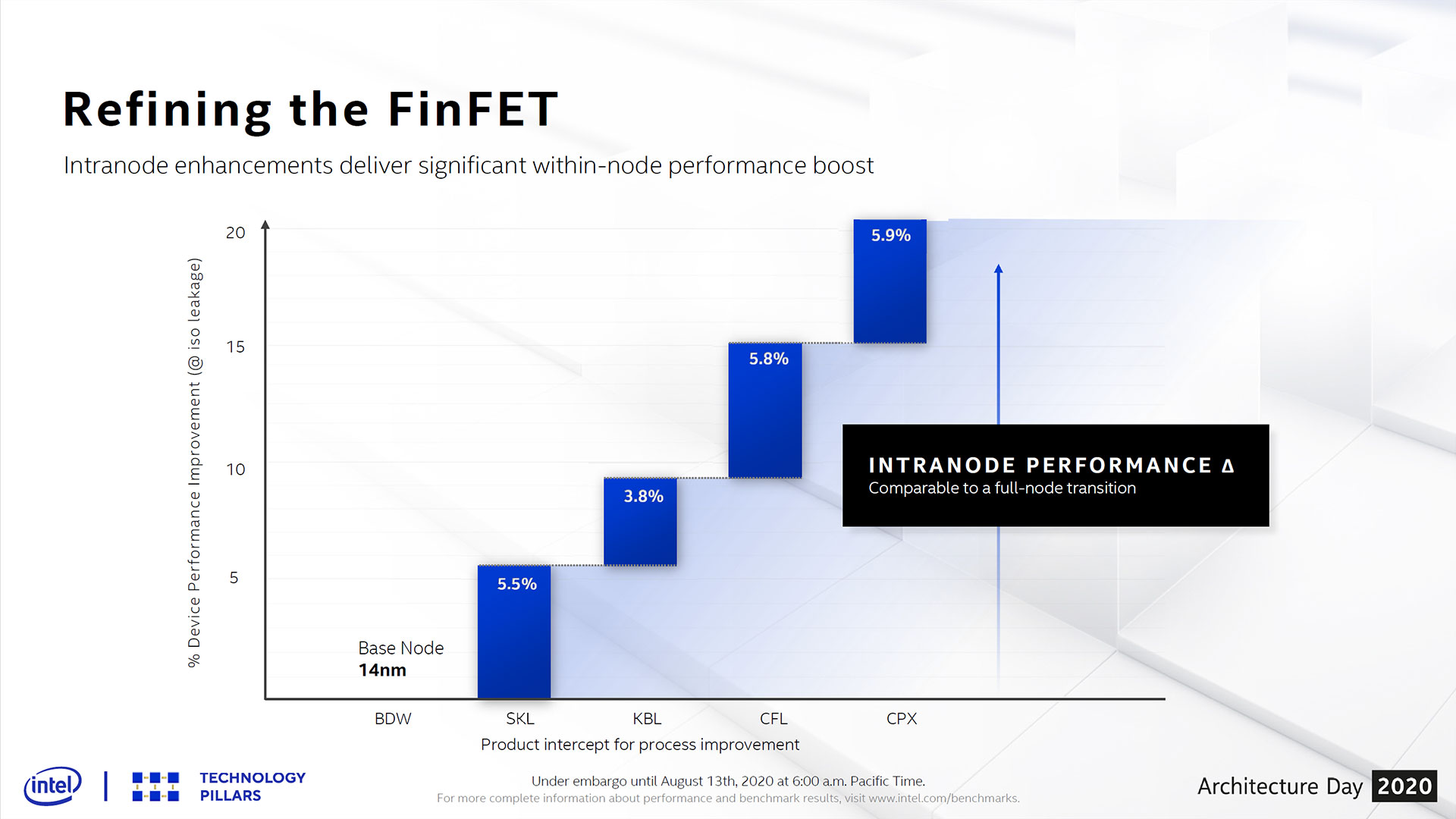
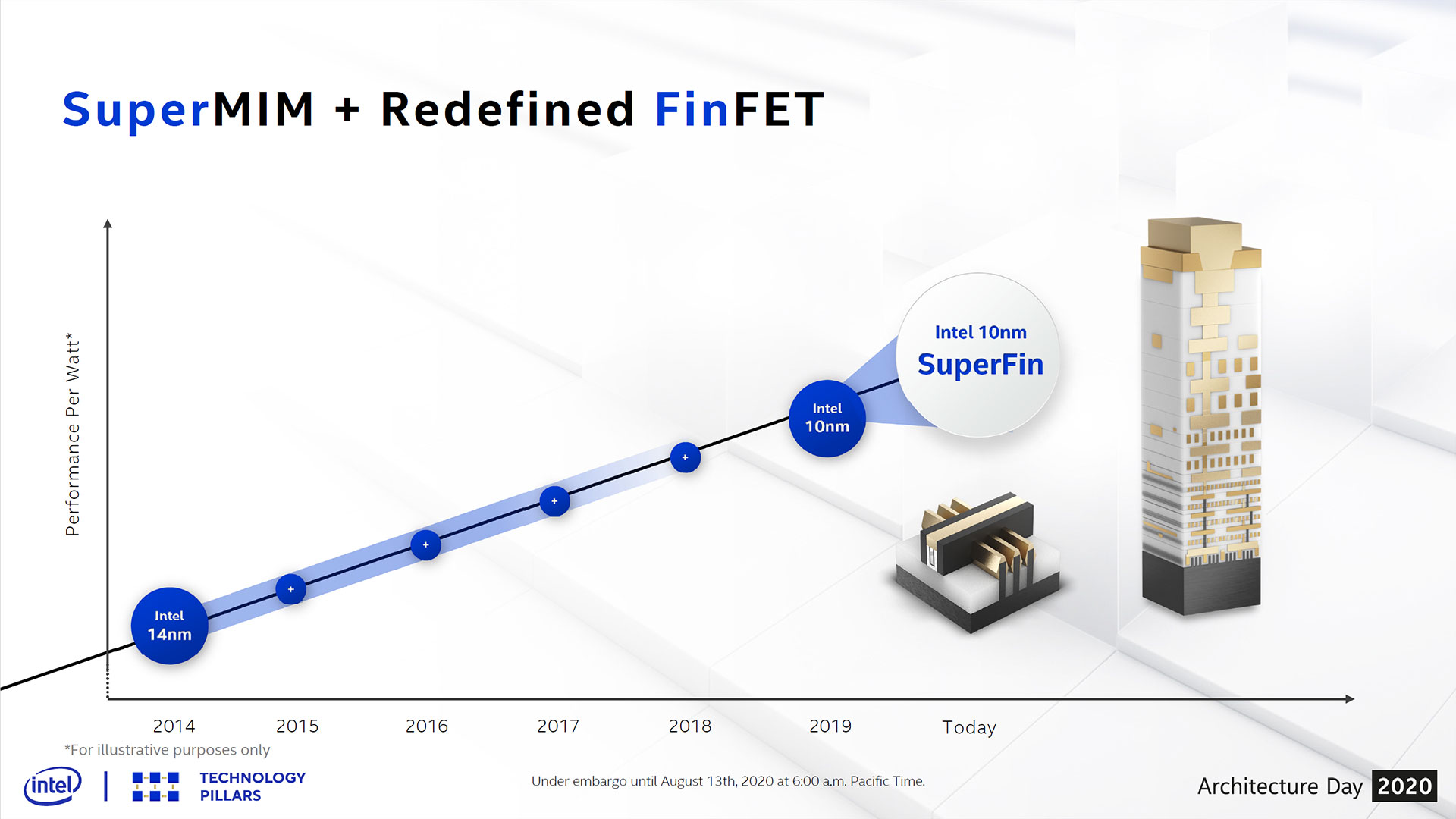
Intel's series of '+' revisions to 14nm, known as inter-node enhancements, have resulted in tremendous improvements over the years through optimizations that include higher drive current, clock speeds, and reduced power density. However, while the chips are now faster than the first 10nm iterations, Intel is still missing out on the transistor density improvements from moving to the smaller node.
Intel isn't clarifying if Rocket Lake comes with yet another new '+' revision of 14nm, but it's fair to assume the chips come with a few more tweaks to the process. Beyond commenting that Cypress Cove and Sunny Cove are essentially the same, Intel hasn't been specific about the differences between the two. It's rational to assume that some alterations to the finer-grained aspects, like instruction and cache timing, among many other factors, had to be adjusted to account for the variations that crop up between 14nm and 10nm due to different transistor sizes, density, and power characteristics.
We do know plenty of details about Sunny Cove, as it did debut three years ago in Ice Lake processors, so we'll do a condensed fly-by.
Sunny Cove includes improvements to every level of the pipeline. Key improvements to the front end include larger reorder, load, and store buffers, along with larger reservation stations. Intel increased the L1 data cache from 32 KiB, the capacity it has used in its chips for a decade, to 42 KiB, and moved from 8-way to 12-way associativity. The L2 cache moves from 4-way to 8-way and is also larger, but the capacity is dependent upon each specific type of product — for Rocket Lake it weighs in at 512 KiB per core. L3 cache remains unchanged and is inclusive, whereas Zen's L3 is exclusive.
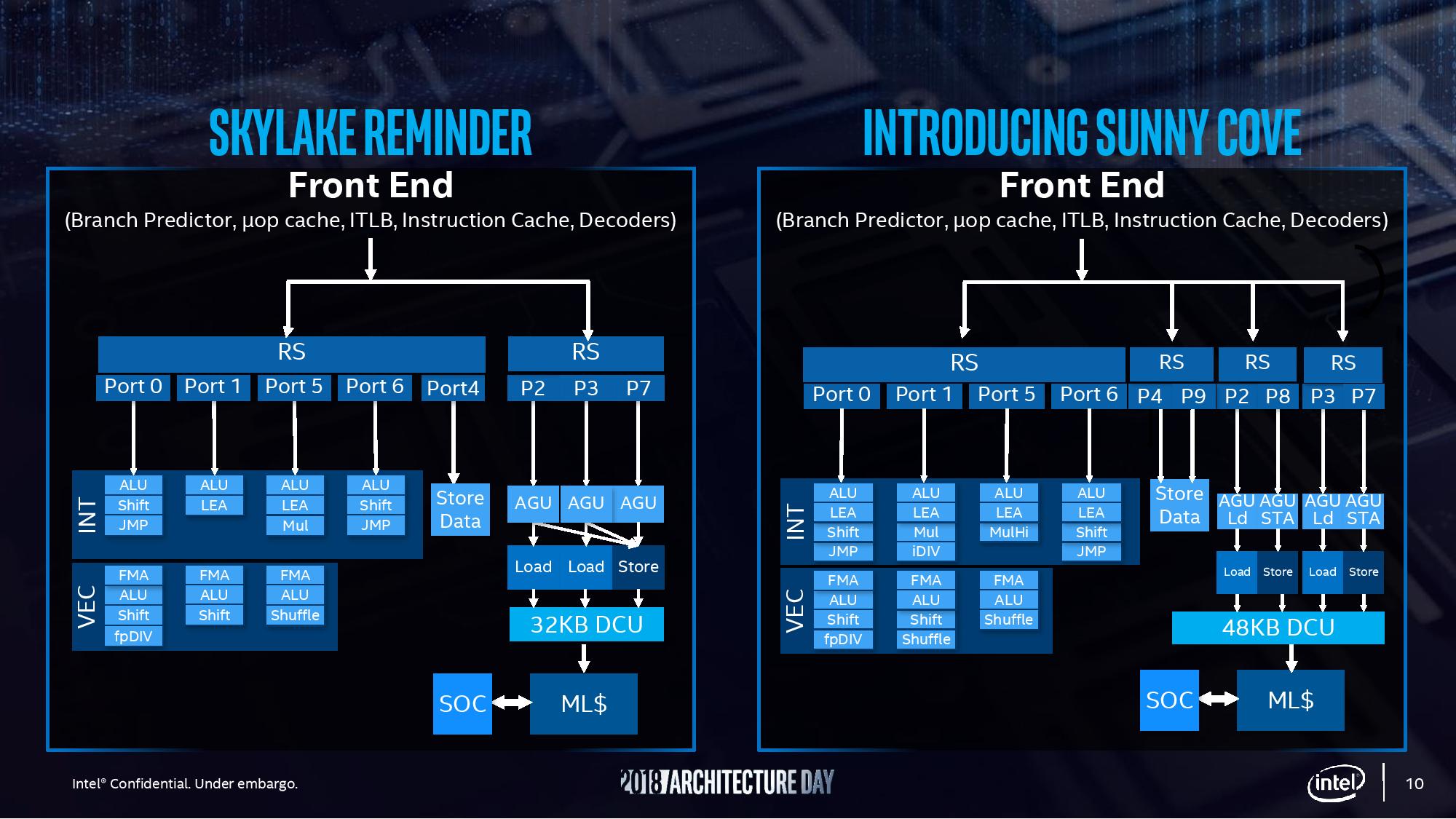
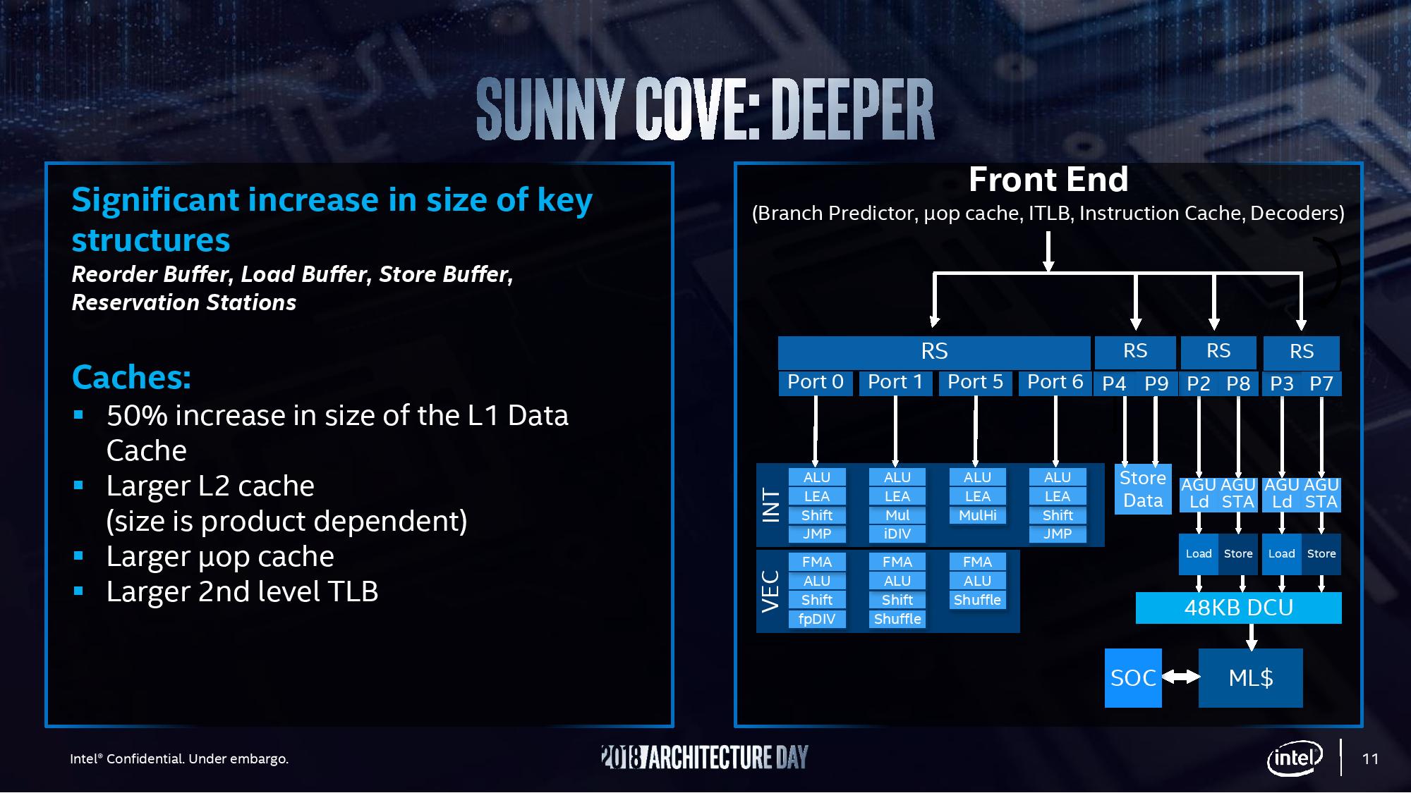
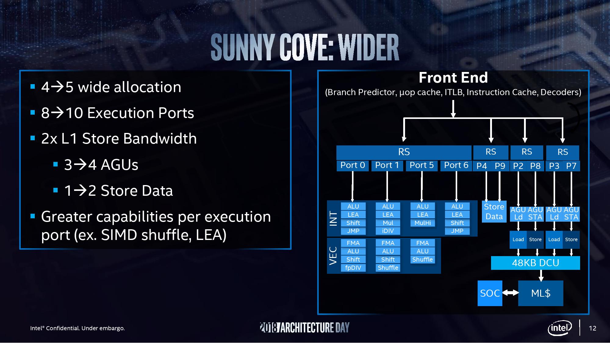
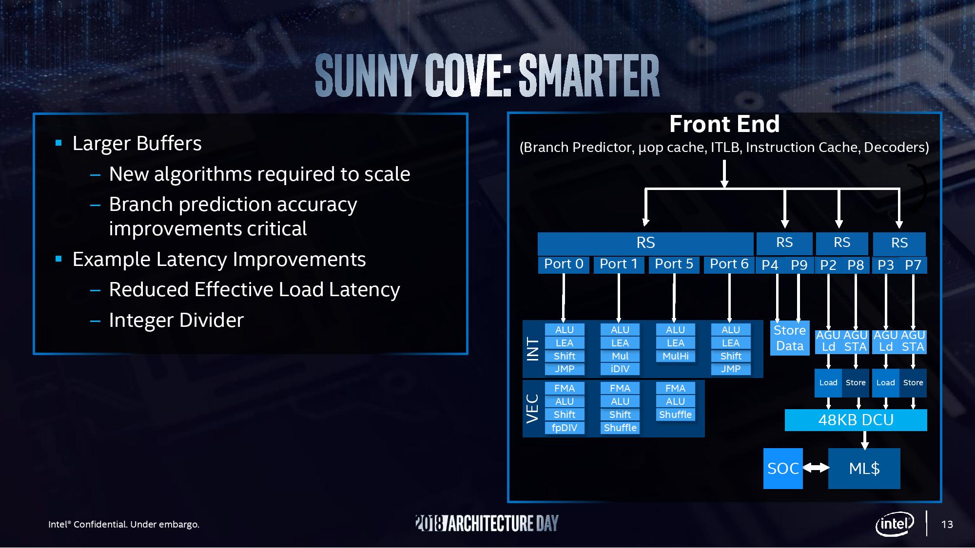
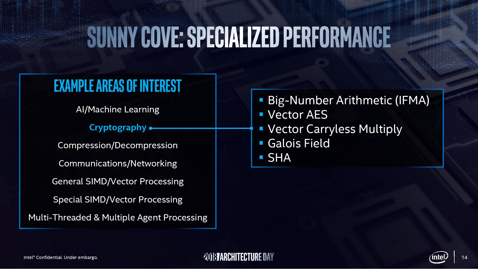
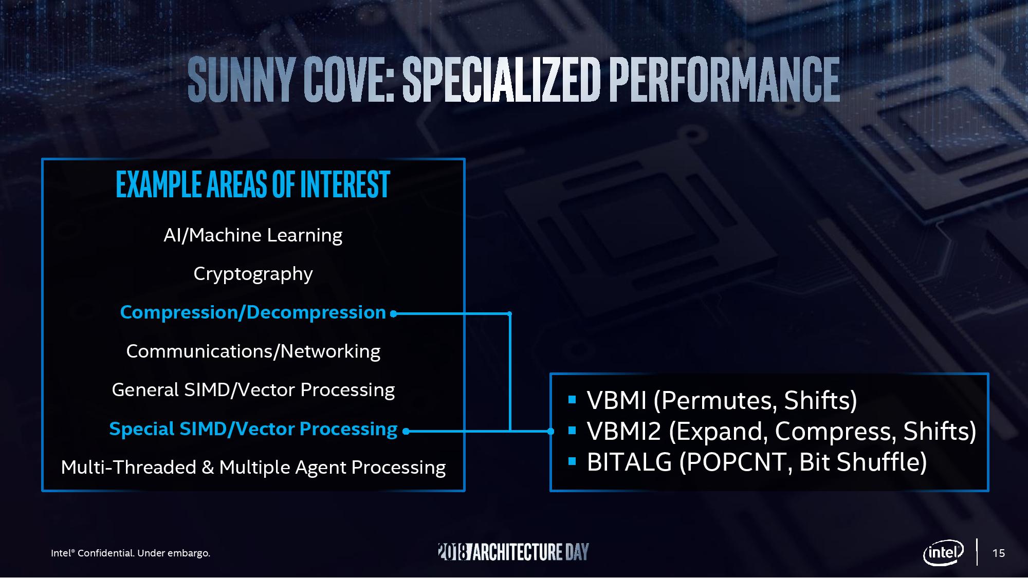
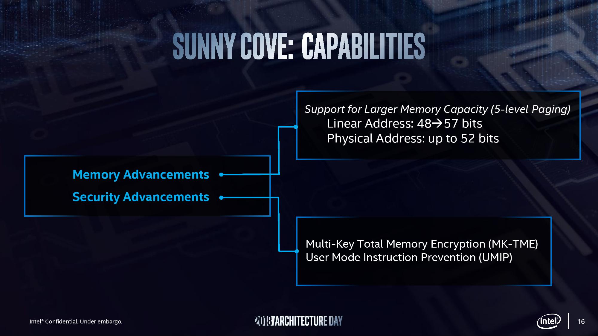
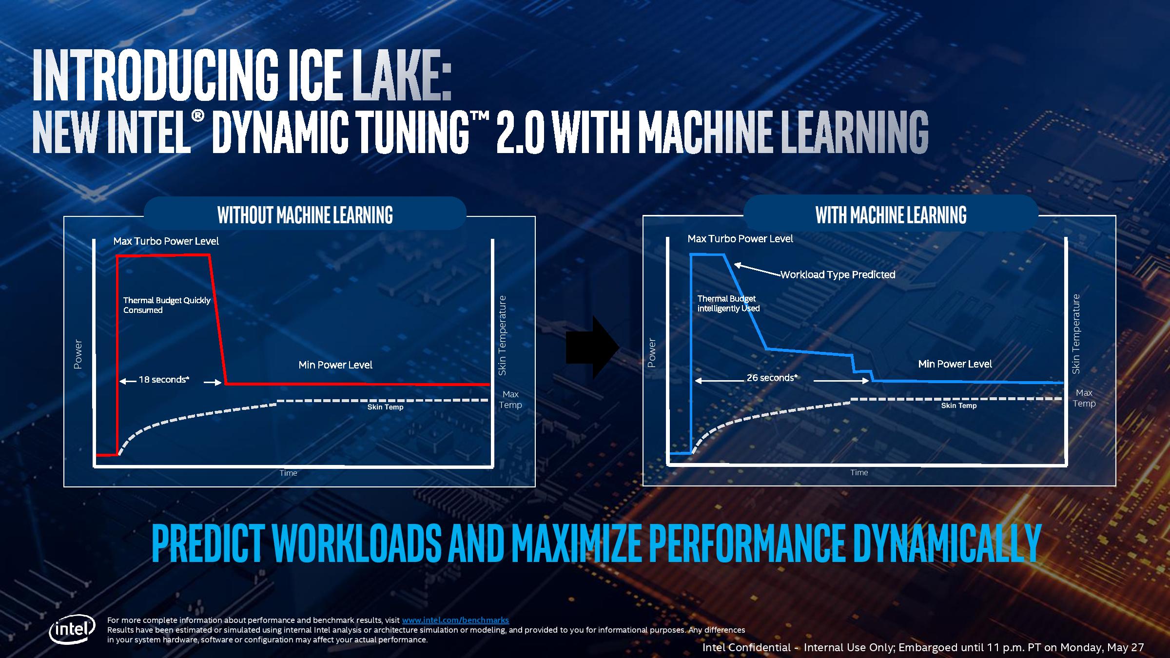
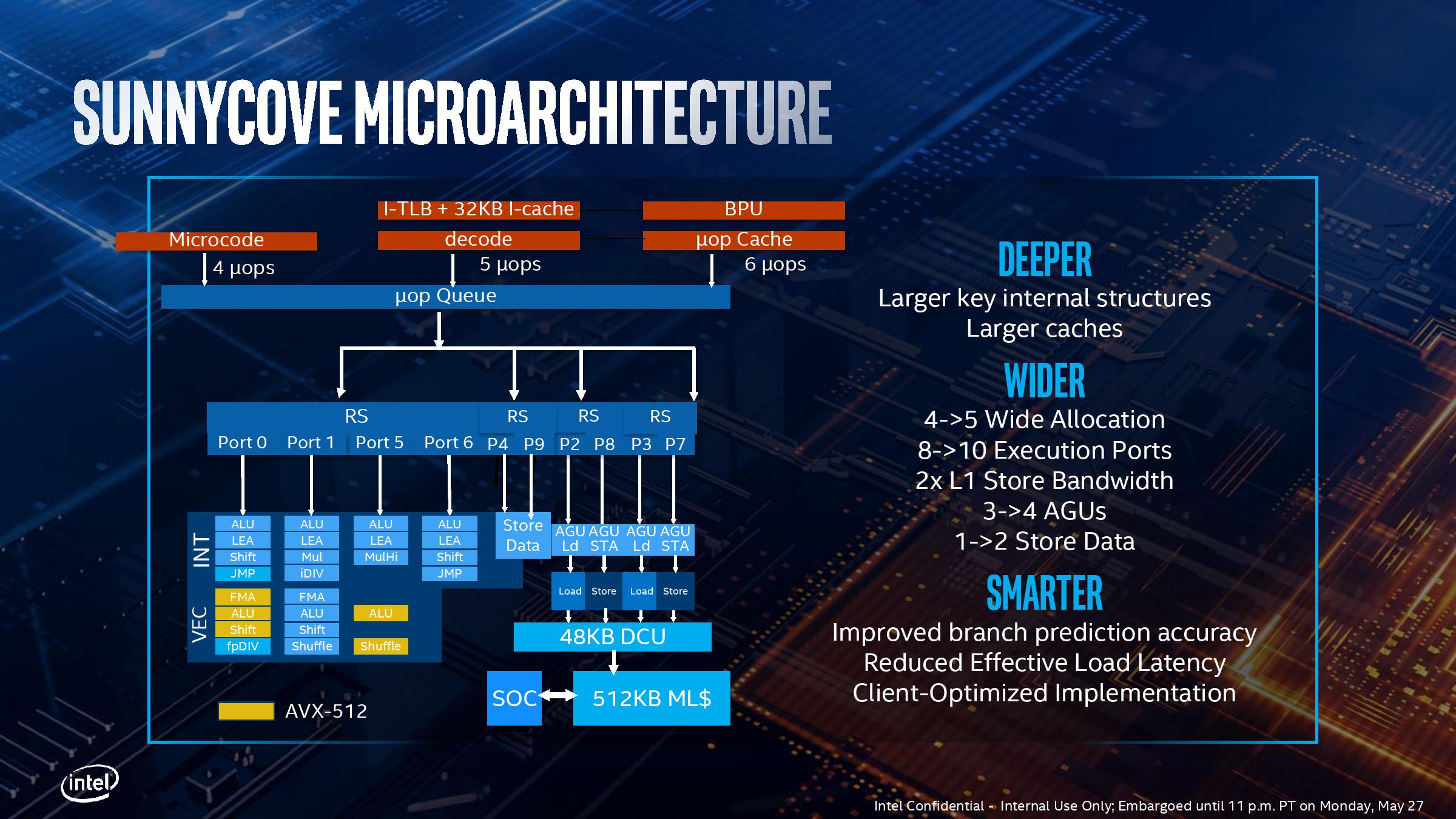
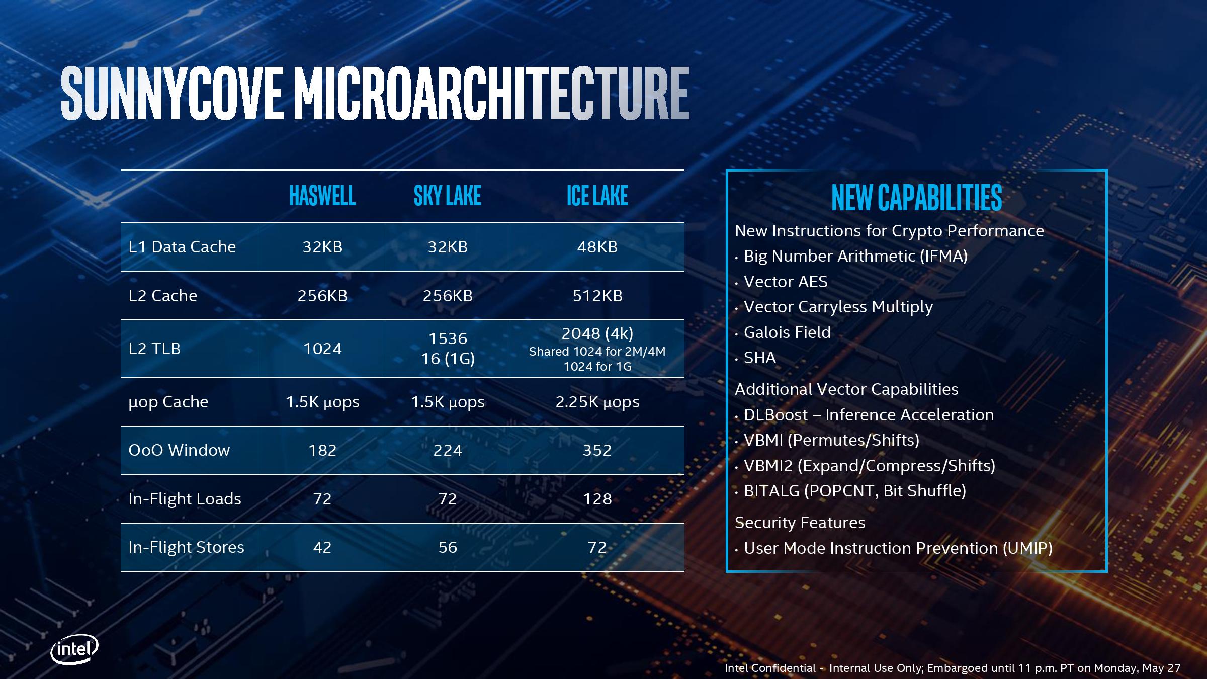
Intel expanded the micro-op cache (UOP) from 1.5K to 2.25K micro-ops, the second-level translation lookaside buffer (TLB) from 1536 entries to 2048, and moved from a four-wide allocation to five-wide to allow the in-order portion of the pipeline (front end) to feed the out-of-order (back end) portion faster. Intel also increased the number of execution units to handle ten operations per cycle (up from eight with Skylake). Intel also focused on improving branch prediction accuracy and reducing latency under load conditions.
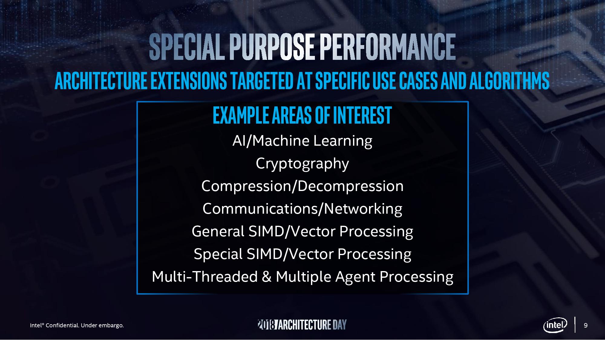
The store unit can now process two store data operations for every cycle (up from one), and the address generation units (AGU) also handle two loads and two stores each cycle. These improvements are necessary to match the increased bandwidth from the larger L1 data cache, which does two reads and two writes every cycle. Intel also tweaked the design of the sub-blocks in the execution units to enable data shuffles within the registers. Support for AVX-512, including Intel's DL Boost tech for AI inference, was also added, along with doubling the peak throughput of AES-NI instructions. For more detail on Sunny Cove, head here.
The net effect of these modifications, naturally, is increased IPC. Here's what that looks like.
Intel 11th-Gen Rocket Lake IPC Measurements
Be aware that IPC measurements can vary drastically based on the types of applications used, instructions in play, and measurement methodology. We tested a limited subset of single-threaded workloads to see the clock-for-clock improvements, locking all chips to a static 3.8 GHz all-core clock with the memory dialed into the officially supported transfer rate.
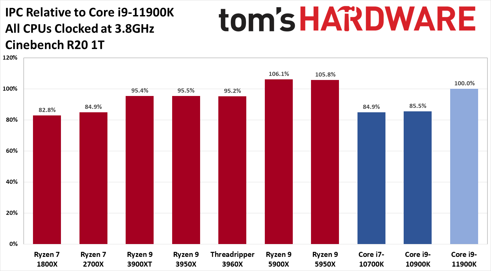
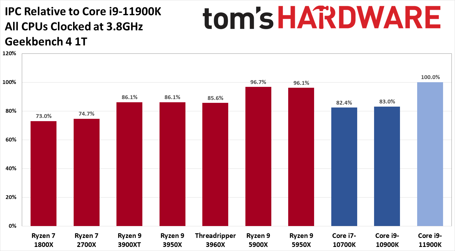
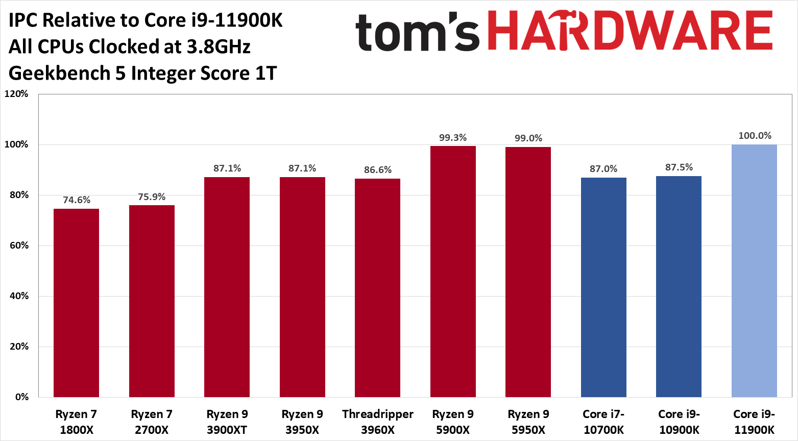
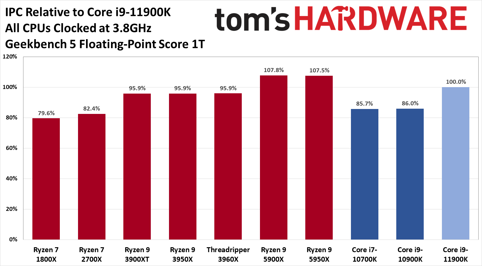
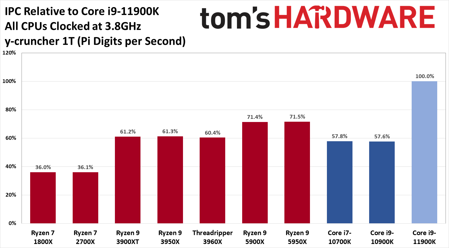
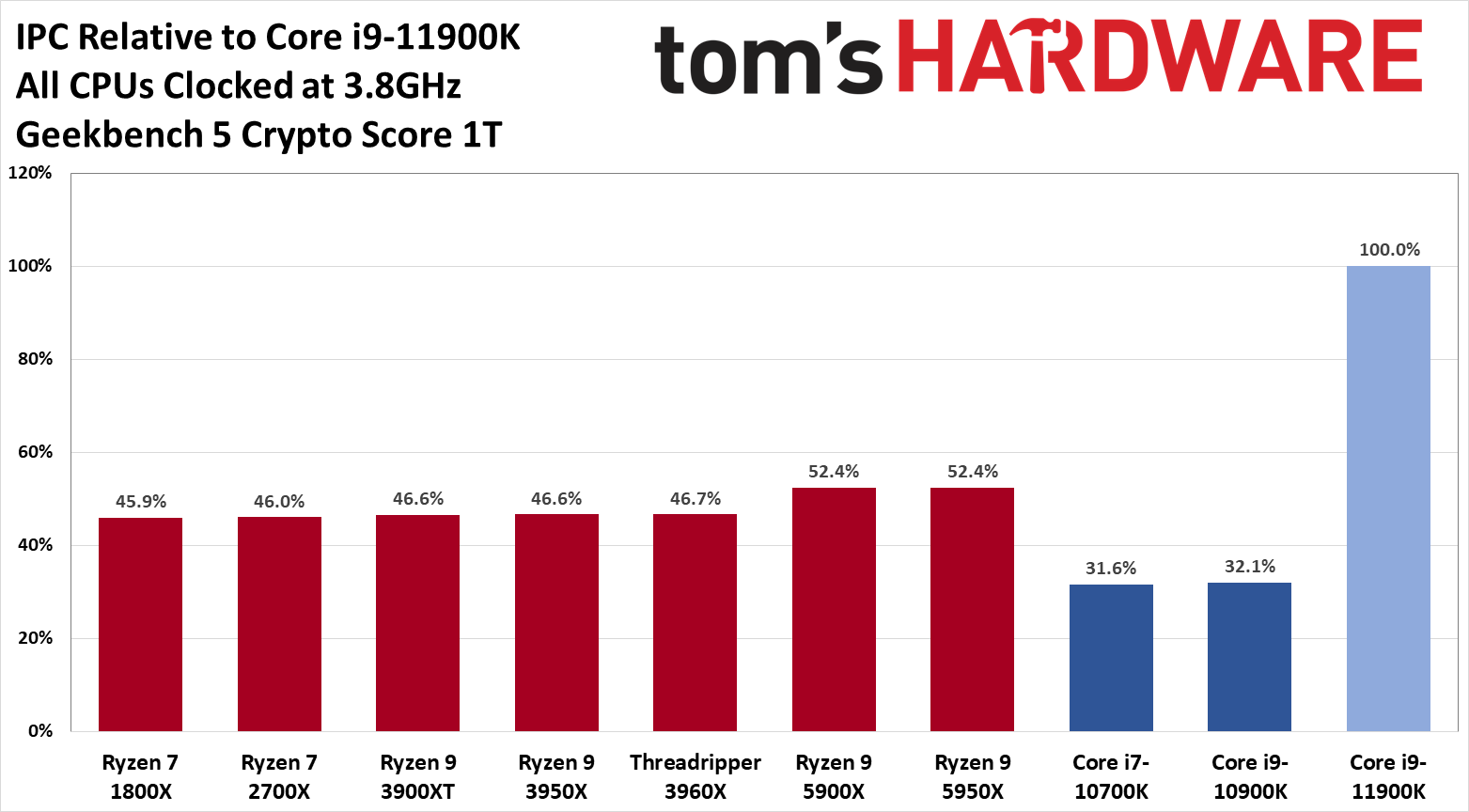
IPC measurements are typically based on an average of a broader swath of workloads, so take our measurements as a general guide. Intel's Cypress Cove microarchitecture has made a big leap forward in several of our tests, with an ~13% to 14% increase over the 10900K in the Geekbench 5 floating point and integer tests, respectively. It still lags the Zen 3-powered Ryzen 5900X by 7.8% in the floating point workload, and essentially ties in the integer test. We also see a 17% increase in the overall Geekbench 4 result over the 10900K and a 3.3% lead over Zen 3. Cinebench shows another solid gain, but Zen 3 (predictably) continues to lead in that workload, too.
Rocket's biggest gains come in the y-cruncher benchmark, which leverages AVX-512, and the Geekbench 5 crypto score, which leans on AES instructions. Both of these were key design points for Cypress Cove, and the results show.
MORE: Best CPUs
MORE: CPU Benchmarks Hierarchy
MORE: All CPUs Content
Current page: Rocket Lake Boost Tech, IPC Measurements, Cypress Cove Architecture
Prev Page Pushing 14nm to the Limit Next Page Intel Rocket Lake Xe Graphics, Motherboards, Gear 1 and 2 Memory, Test Setup
Paul Alcorn is the Editor-in-Chief for Tom's Hardware US. He also writes news and reviews on CPUs, storage, and enterprise hardware.
-
Zacca You have forgotten to post SolidWorks graphs. And Creo is wrongly posted in the Workstation stackReply -
Zacca ReplyAdmin said:We put the Core i9-11900K and Core i5-11600K to the test in our gaming and application benchmarks.
Intel Core i9-11900K and Core i5-11600K Review: Rocket Lake Blasts Off : Read more
Once again, please add the missing SolidWorks graphs to the SPECviewperf 2020 benchmark image stack. Also Creo is miss placed.
