


A Little History Of Intel's Pentium II
Before we get into the details of the SL2W8, we should first recap the history of the PII 300.
- Die Size
A few months after the first launch of Intel's Pentium II as 233 and 266 MHz version in Q2 1997, Intel released the PII 300. At this time the Pentium II was manufactured using the .35 micron technology. The code name of the Pentium II chip from this time was 'Klamath'. At the beginning of 1998, Intel introduced the 333 MHz PII, followed later by the 350, 400 and 450 MHz version. The 333 MHz PII and up was not using the older .35 micron Klamath core anymore, but the new 'Deschutes' core, a chip produced using the .25 micron technology. The 'Deschutes' core is not much different to Klamath in terms of its functionality, both chips are Pentium II chips and perform equally. The difference is subtler and is also not simply defined by the core. Klamath has a larger die size, due to the .35 micron technology, which you can see by having a look at the chips.
- Klamath
PII 233 - 300
- Deschutes
PII 333 - 400
- Core Voltage
The next difference between the chips is the voltage they are running at, the Klamath is using 2.2 V, the Deschutes runs at only 2 V. The die size and the voltage difference are both responsible for the difference in heat production. Klamath becomes a lot hotter than Deschutes, making overclocking of Klamath a lot harder than overclocking Deschutes.
- Tag RAM Chip 82459
That is not the only difference between older and new PII CPUs, there is also the L2 cache controller. As you all know, the Pentium II has got a L2 cache within its cartridge, running at half the processor clock. This L2 cache needs a L2 cache controller, because Intel did not include one into the Pentium II core. One of the important things about L2 cache controllers is its cacheable area. The combined L2 cache controller / tag RAM chip used together with Klamath chips on PII 233 - 300 MHz used to be the '82459AB'. This chip could only cache up to 512 MB of memory, so that those Pentium II CPUs could not run with more memory than 512 MB. The first Pentium II 333 CPUs came with the '82459AC' L2 cache controller/tag RAM chip, which can run at higher clocks, but it is still only able to cache 512 MB. Later the PII 333 and all faster PII CPUs (350,400,450 MHz) were equipped with the '82459AD', which is not only able to keep up with up to 225 MHz L2 clock speed, but it can finally cache up to 4 GB of memory. Intel's internal name for the 82459AD is 'tp6e'.
- L2 Cache
The third difference between the PII CPUs is the L2 cache that is used. Klamath (PII 233 - 300) used to come with four L2 cache chips rated at 6.5 or 7 ns, thus good enough for L2 cache clocks of 140 MHz (7 ns) or 150 MHz (6.5 ns). The PII 333 is normally using two 5.5 ns L2 cache chips, rated for up to 180 MHz, the 350 and 400 MHz versions come with two 5 ns chips, good for 200 MHz and finally the PII 450 is equipped with 4.4 ns chips, rated for 225 MHz. This difference if of major importance, since the L2 cache is a sensitive part of the Pentium II. Running it way beyond spec will most likely cause L2 cache errors and thus system crashes, even if the CPU core is doing fine at this speed.
- Microcode and Intitialization
Finally the last major difference is the microcode update and the CPU initialization that's done each time you boot your system. Different chip revisions have different microcode updates (the code that is loaded into a special CPU-area to fix minor CPU bugs) and, more importantly, different chip revisions have different initialization routines at each different CPU clock. When the system is booting, there are several undocumented CPU 'registers' read by the BIOS, which then sets the L2 cache timings and other things according to the information read from the CPU. This routine cannot be cheated by anyone except the motherboard maker, because nobody knows what information is read and how to react to it.
So far about the basics.
The Pentium II 300 SL2W8
I already mentioned in the introduction, the 'SL2W8' is almost a Pentium II 450. Why do I say that?
Well, first of all, not each SL2W8 is equipped the same. In the past Intel used an S-spec to clearly define a CPU core and its equipment, now it only seems to be a 'name' for a family of CPUs, which are not all quite the same. What can be stated about SL2W8 however, is that all CPUs with that S-spec have a 'Deschutes' core, thus producing a lot less heat than older PII 300 CPUs and also running at only 2 V. The second fact is that the SL2W8 comes with the 'tp6e', the fast 4 GB L2 cache controller / tag RAM.
Those two facts are already quite encouraging for overclockers, because we know that Deschutes is willing to run up to at least 400 MHz in most cases, as well known from the old Celeron chips. You certainly remember, the Celeron without L2 cache was nothing but a pure Deschutes chip, running up to 400 or even 450 MHz when overclocked. The L2 cache controller that's even used inside the PII 450 is certainly a part that will run up to 450 MHz and having a cacheable area of 4 GB instead of only 512 MB as in the old PII 300 CPUs is certainly a nice thing too.
The touchiest thing in terms of overclocking a Pentium II is the L2 cache though. Here the SL2W8 varies unfortunately. Some SL2W8 CPUs come with 5.5 ns L2 cache, some with 5 ns, but there is a whole lot that is equipped with 4.4 ns L2 cache modules!!! You can imagine, the SL2W8 chips with 4.4 ns L2 cache are more or less supposed to run at 450 MHz or even more. The ones with only 5 or 5.5 ns are still equipped with a faster cache than what is needed for 300 MHz (6.5 ns), so that you can certainly overclock them, however not all to 450 MHz reliably.
Before you get all worked up about this, please realize that even a SL2W8 with 4.4 ns L2 cache is not a real PII 450. The PII 450 comes with a new packaging of the core chip, called 'OLGA' or 'flip chip'. The PCB of the PII 450 is also different from the PCB of a 'normal' Deschutes' PCB, as found in PII 333 - 400.
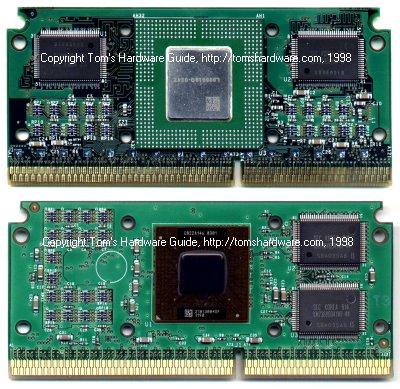
Above you can see the PII 400 with its typical core packaging and the PCB with the L2 cache modules left and right of the CPU core. This is what SL2W8 looks like as well. Underneath you can see the 'real' PII 450, with the flipchip packaging and both L2 cache modules on the right of the CPU core. The flipchip packaging ensures even better heat conduction than the old packaging above.
Another important difference is the aluminum plate that covers the board on the side you are looking at on the above picture and that's supposed to conduct the heat between the chips and the heat sink. Intel calls that plate T-plate, and there are three different types available.
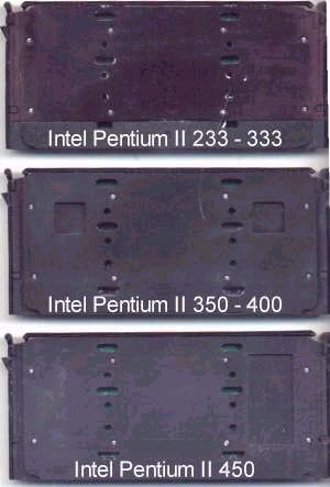
That's what the cartridges look from the outside, looking at the T-plates. The upper T-plate is simply plane and connects only to the CPU core on its other side. This T-plate is used for PII 233 - 333. The T-plate in the middle is for PII 350 and 400. It has two notches, which connect to the L2 cache modules on the other side. The T-plate below belongs to PII 450, touching the two L2 cache modules on the right side of the CPU core. As being an official PII 300, SL2W8 is unfortunately equipped with the T-plate at the very top, thus it's not cooling the L2 cache modules. This is of course an issue if you want to run it at 450 MHz or more, because your heat sink doesn't cool the L2 cache, as done in every PII 350 - 450.
Whilst there isn't a work around for the flip chip issue, you can certainly do something about the T-plate. You have to open up the cartridge though, and then place an aluminum plate of the right thickness between the L2 cache chips and the T-plate, fixing it with some thermal compound. You could also use some coins, but the only ones I found with the right size are coins of 20 Greek Drachmas, 10 French Francs or 50 Hong Kong Dollars and you need more thermal compound to fill the gaps in the coins.