ATI Radeon HD 4770: 40nm Goes Mainstream
Get Tom's Hardware's best news and in-depth reviews, straight to your inbox.
You are now subscribed
Your newsletter sign-up was successful
Radeon HD 4770: Speeds And Feeds
Superficially, the Radeon HD 4770’s specs look fairly similar to ATI’s Radeon HD 4830. But they’re completely unique GPUs. For example, the 4830 centers on the familiar 956 million transistor RV770 with two of its 10 SIMD units disabled, yielding 640 total stream processors and the ability to filter 32 textured pixels per clock (down from 800 and 40, respectively).
ATI’s Radeon HD 4830 retained all four of the RV770’s render back-ends (each of which could process four pixels and 16 Z/stencil operations per clock—that’s why you see these cards spec’ed out with 16 ROPS). The memory controllers carried over as well, enabling the same 256-bit memory bus employed on Radeon HD 4850 and 4870 boards. The main difference, of course, was that the 4850 and 4830 were only armed with GDDR3, while the 4870 sported GDDR5.
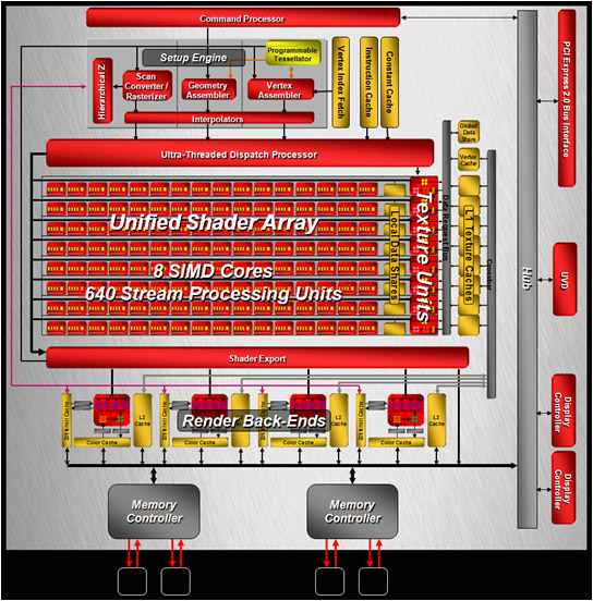
In comparison, the Radeon HD 4770’s architecture employs an 826 million transistor GPU armed with the same number of SIMD units available (eight). It also boasts 640 stream processors (128x5) and 32 texture units. So, from a front-end view, RV740 looks a lot like the RV770 after it was chopped up to become Radeon HD 4830.
The full complement of ROPs carries over too, processing 16 pixels and 16 Z/stencil ops per clock. Where you’ll notice the most significant difference is the memory configuration—two of the four 64-bit controllers are cut, leaving a 128-bit pathway. Because those memory controllers are connected to the render back-ends via a hub, they don’t need to be mapped on a 1:1 basis.
Now, you’d assume the halved memory bus (down from 256-bits) would hammer performance. But ATI is outfitting the Radeon HD 4770 with 512 MB of GDDR5 memory, able to move twice as much data per clock versus GDDR3. So, the 4770’s throughput actually turns out to still be respectable for a mainstream part.
The shift to 40 nm has seemingly allowed ATI to push clocks on its Radeon HD 4770 significantly higher than what it was willing to offer on the 4830. Stock, the GPU runs at 750 MHz (versus the 4830’s 575 MHz).
Though the 800 MHz memory clock would appear slower than the 4830’s 900 MHz operating frequency, it’s important to remember that GDDR5 provides doubled I/O throughput. Of course, the card’s 128-bit counteracts those benefits. Whereas Radeon HD 4830 served up roughly 57.6 GB/s, the 4770 pushes 51.2 GB/s.
Get Tom's Hardware's best news and in-depth reviews, straight to your inbox.
Another benefit of the 40 nm transition is reduced board power. ATI claims the 4770 is rated for a maximum 80W, putting it just over what a PCI Express slot is able to supply on its own. That’s well under the 110W cited for the Radeon HD 4850, though—a board that we’ll see is within the 4770’s performance crosshairs.
| Header Cell - Column 0 | Radeon HD 4850 | Radeon HD 4830 | Radeon HD 4770 | Radeon HD 4670 | GeForce GTS 250 |
|---|---|---|---|---|---|
| Manufacturing Process | 55 nm TSMC | 55 nm TSMC | 40 nm TSMC | 55 nm TSMC | 55 nm TSMC |
| SPs | 800 | 640 | 640 | 320 | 128 |
| Core Clock | 625 MHz | 575 MHz | 750 MHz | 750 MHz | 738 MHz |
| Shader Clock | 625 MHz | 575 MHz | 750 MHz | 750 MHz | 1,836 MHz |
| Memory Clock | 1,000 MHz GDDR3 | 900 MHz GDDR3 | 800 MHz GDDR5 | 1,100 MHz GDDR4 | 1,100 MHz GDDR3 |
| Frame Buffer | 512 MB | 512 MB | 512 MB | 512 MB | 1 GB |
| Memory Bus Width | 256-bit | 256-bit | 128-bit | 128-bit | 256-bit |
| ROPs | 16 | 16 | 16 | 8 | 16 |
| Price | ~$129 | ~$90 | $109 | $80 | ~$129 |
Current page: Radeon HD 4770: Speeds And Feeds
Prev Page Introduction Next Page Overclocking And Cooling-
Dekasav "Well-played ATI, well played."Reply
Couldn't say it better, myself.
Looks to be a pretty good card, but nothing spectacular. 40nm is nice, a little cheaper HD 4850 (fewer FPS, too), but all in all, nicely done.
I wonder who'll sell more, now, the 4850 or the 4770? -
"The card’s strange behavior continues on the CPU-only test, where it takes a nearly 2,000-point hit for no good reason" maybe because of the 128 bit memory busReply
-
bardia I'm pretty blown away at the kind of performance that can be had for ~$100 these days thanks to ATI. It wasn't long ago when Nvidia forced us to choice between the incredibly crappy 8600GT for $150 and the ~$250-300 8800GTS 320.Reply
ATI is leading us into graphics nirvana. -
pharge Wondering will 4770 a good one for crossfire? Can we have a review on it....? With its low power useage when fully loaded, cheaper price (~$40 cheaper than 4850 when CF), not much slower than 4850 (512MB), and nice overclocking range... It will be nice to see will 4770 CF setup be useful (playable) in games (1920x1200) with some visual goodies truned on.Reply
-
Summer Leigh Castle bardiaI'm pretty blown away at the kind of performance that can be had for ~$100 these days thanks to ATI. It wasn't long ago when Nvidia forced us to choice between the incredibly crappy 8600GT for $150 and the ~$250-300 8800GTS 320.ATI is leading us into graphics nirvana.I spent almost $300 on my 8800GTS 320 OC when they came out and I thought I got a great deal. Things have changed! Competition = good for the consumers!Reply
-
eklipz330 this card is amazing for 1680x1050, if they can manage to slap some aftermarket coolers on there, buying two for the price of a 1gb 4870, and overclocking them, im pretty sure we'd pass gtx 285 numbers.... simply amazing.Reply
great card for 16x10 resolution. good job ati, you've done more damage to nvidia in the past year than they've done to you in the pass 3-4 -
eklipz330 *edit*Reply
just checked newegg and they all have aftermarket coolers on them... wow *_*
http://www.newegg.com/Product/ProductList.aspx?Submit=ENE&DEPA=0&Order=BESTMATCH&Description=4770&x=0&y=0 -
Ryun eklipz330*edit*just checked newegg and they all have aftermarket coolers on them... wow *_*http://www.newegg.com/Product/Prod 70&x=0&y=0Reply
Nah, they're reference coolers from AMD. From what I heard, AMD gave the AIB partners a choice between the dual slot and the, for lack of a better term, uglier cooler. Apparently the "uglier" one is cheaper so that's what you're probably going see for now.


