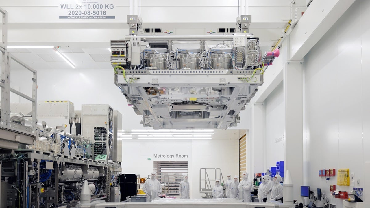
Samsung rep says High-NA EUV is good for logic fabrication but might have cost issues for memory — Intel, ASML, and others share more bullish views
SPIE panel discusses the future of EUV.

At the SPIE Advanced Lithography + patterning conference in San Jose, California, experts from different sectors of the lithographic ecosystem discussed the prospects of Low-NA and High-NA extreme ultraviolet (EUV) lithography. Their views ranged from highly optimistic to cautious, particularly regarding High-NA EUV. For memory production, a Samsung rep noted worried about the costs associated with High-NA EUV.
Young Seog Kang, a Fellow at Samsung involved with memory production, said that Low-NA EUV is already operational, and chip manufacturers might prefer using double patterning with Low-NA EUV or resorting to advanced packaging techniques as more economical alternatives rather than using High-NA EUV. For memory, he predicted a shorter lifespan for EUV in general, citing potential challenges in performance and cost when trying to extend the technology. However, he acknowledged that EUV might remain relevant longer for logic chips due to their more complex layouts.
"As a user, I am always concerned with total cost," Kang said.
One of the challenges with post-3nm production technologies is the necessity to lower critical dimensions (i.e., increase resolution) produced by lithography systems from 13nm to 8nm. This could be done by employing EUV machines with projection optics featuring a 0.55 numerical aperture (High-NA); using double patterning with EUV systems with projections optics featuring a 0.33 NA (Low-NA); or by using pattern shaping systems like Applied Materials's Centura Sculpta (which allows reducing EUV double patterning steps but does not eliminate them or the use of High-NA EUV); and by enhancing other process-related factors, such as photoresist properties, illumination settings, and mask enhancements.
Intel plans to adopt High-NA EUV lithography and Applied's Centura Sculpta for its upcoming process technologies (Centura Sculpta starting at 20A and High-NA EUV starting at 14A); other chipmakers are researching High-NA EUV.
There are other potential paths to increased capabilities and lower costs with EUV — Intel's Frank Abboud, vice president and general manager of mask operations, discussed employing phase shift masks to enhance EUV lithography. Such masks, beneficial in DUV lithography, use phase differences to improve image resolution. Although phase shift masks have not yet been developed for EUV, Abboud believes they are achievable.
Jan van Schoot, director of system engineering at ASML, outlined several approaches to enhance the resolution and extend the utility of EUV lithography. In addition to increasing the numerical aperture of projection optics, it is possible to optimize k1, a coefficient that represents a lithography system's resolution capability. This could be done using various methods, including photoresist qualities, illumination settings, and mask enhancements. He said ASML is actively working on a new illuminator and other strategies to improve k1, and the company has some promising ideas in the pipeline.
Get Tom's Hardware's best news and in-depth reviews, straight to your inbox.
Mark Slezak, the president of JSR USA (a photoresist supplier), suggested that EUV technology could last 20 years. He drew parallels with the extended use of DUV lithography, which lasted much longer than anticipated due to innovations like immersion lithography and multi-patterning. Slezak believes similar advancements could prolong EUV's relevance, with High-NA EUV being a potential example.

Anton Shilov is a contributing writer at Tom’s Hardware. Over the past couple of decades, he has covered everything from CPUs and GPUs to supercomputers and from modern process technologies and latest fab tools to high-tech industry trends.
-
scottslayer ReplyMark Slezak, the president of JSR USA (a photoresist supplier), suggested that EUV technology could last 20 years. He drew parallels with the extended use of DUV lithography, which lasted much longer than anticipated due to innovations like immersion lithography and multi-patterning. Slezak believes similar advancements could prolong EUV's relevance, with High-NA EUV being a potential example.
I assume everyone at the meeting looked at each other very nervously because those "innovations" for DUV were deperately needed because EUV was heavily delayed.
EUV and High-NA are going to need to stick around because next gen Hyper-NA is reportedly extremely expensive (500 million per machine at least) and companies are getting antsy with the costs. -
Steve Nord_ Probing Hydrodynamic Fluctuation-Induced Forces with an Oscillating RobotReply
Steven W. Tarr, Joseph S. Brunner, Daniel Soto, and Daniel I. Goldman
Phys. Rev. Lett. 132, 084001 – Published 20 February 2024 What was spammy abt. saying running from flash was how this started or calling DUV exposure units dead raccoons!