Intel Shows Off Meteor Lake Test Chips
Intel's 2023 Meteor Lake already running through Fab 42.

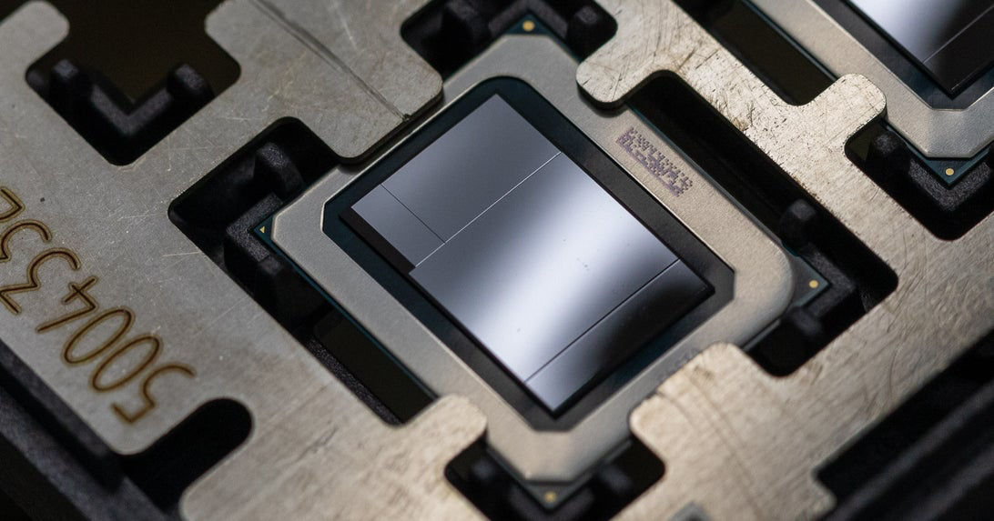
Intel has demonstrated a prototype of its codenamed Meteor Lake processor that is due in 2023. The 14th Generation Core CPUs will be the company's first client processors that will use a multi-chiplet design. Right now the company is testing interconnection technology that will bridge all of Meteor Lake's pieces together.
Stephen Shankland from CNET had a rare opportunity to visit Intel's leading-edge Fab 42 near Chandler, Arizona, and take pictures of Intel's upcoming Meteor Lake, Sapphire Rapids and Ponte Vecchio products. Intel's Arizona camp is where the company produces its most advanced processors using its 10nm, 10nm SuperFin, and 10nm Enhanced SuperFin (now called Intel 7) nodes as well as uses its advanced chip packaging technologies.
Intel powered on a Meteor Lake compute tile (made using EUV-enhanced Intel 4 fabrication technology) just over a month ago. The pictured Meteor Lake CPU sample is used to test its interconnection technologies used to glue all parts together.
Previously, Intel said that its codenamed Meteor Lake processor consists of three tiles: a compute die with an unknown number of Ocean Cove high-performance cores and energy-efficiency cores, a GPU die with 96 EUs – 192 EUs, and an SoC die packing such units as a memory controller, a PCIe controller, and a Thunderbolt controller. Meanwhile, the test chip evidently has four tiles (or chiplets). It's unclear what the fourth tile does.
So far, Intel has only disclosed that Meteor Lake's compute die will be produced using its own Intel 4 manufacturing technology (previously known as 7 nm), whereas the SoC die will be fabbed using a low-power node. These test chips use Intel's second-gen Foveros tech to stack, showing that the chips not only consist of four tiles, but those tiles are also 3D-stacked onto a base tile.
Get Tom's Hardware's best news and in-depth reviews, straight to your inbox.

Anton Shilov is a contributing writer at Tom’s Hardware. Over the past couple of decades, he has covered everything from CPUs and GPUs to supercomputers and from modern process technologies and latest fab tools to high-tech industry trends.
-
Co BIY Interesting picture. I though the point of the chiplet concept was to allow the building of the individual parts separately (different specialized wafers, even separate fabs and nodes) and then "package" them together. Here they are all together on a wafer waiting to be cut. I assume that means they are assembled on top of the base wafer and further processed while the base wafer is it is still whole.Reply -
dalek1234 ReplyCo BIY said:Interesting picture. I though the point of the chiplet concept was to allow the building of the individual parts separately ...
If you are right, then that would most likely mean expensive chip to produce due to poor yields, unless Intel can disable defective components without sacrificing performance of the good parts around. This will make it difficult to compete on price. -
Co BIY Replydalek1234 said:If you are right, then that would most likely mean expensive chip to produce due to poor yields, unless Intel can disable defective components without sacrificing performance of the good parts around. This will make it difficult to compete on price.
Now that I have reviewed all the very interesting photos in the CNET link I see that the individual chiplets are "built" separately but then "assembled" on their substrate wafer while it is still whole. After the chiplets are "bonded" to the substrate wafer then the assembled chips are cut.
Interesting and pretty amazing process. An entire fab is dedicated to that process alone.
Apparently the Meteor Lake Test chips pictured are package testing chips only. They are not functioning silicon off the Intel 4 process.
