Gigabyte Z370 Aorus Gaming 5 Review: Big Flash, Medium Cash
Why you can trust Tom's Hardware
Software & Firmware
The Z370 Aorus Gaming 5’s software suite is the same one we gave we talked about in our Gaming 7 review. App Center remains the launch point for interesting Gigabyte utilities including RGB Fusion and Easy Tune. The Gaming 5 even includes the Gaming 7’s Creative SoundBlasterX 720° audio suite.


The Z370 Aorus Gaming 5’s five lighting zones can be changed individually, but the software doesn’t support color chase or wave modes for onboard LEDs. As for Easy Tune, its automatic algorithm pushed our CPU to 4.9 GHz at around 1.42V, where it promptly thermal throttled under Prime95. Manual tuning works only after clearing auto-tune settings or else the program will lock the OS upon using its “apply” button. After rebooting to load firmware defaults, we restarted Easy Tune and played with clocks and voltage to our heart’s content.
Firmware
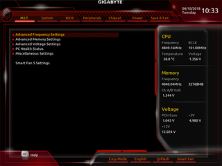
Z370 Aorus Gaming 5 firmware uses its Classic GUI by default, which has popups on the right and bottom to show basic stats and interface options. Its M.I.T. menu is a launch point for submenus that contain most of the settings overclockers need to perform their tuning wizardry.

Among the CPU overclocking menus are a few quick setting configurations that include 4.8 GHz at 1.26 through 1.33V (1.30V fully loaded), 4.9 GHz at 1.26 through 1.36V (1.30V fully loaded), at 5.0 GHz at 1.27 through 1.38V (1.32V fully loaded). Given that the 4.8 GHz setting kept our CPU at 1.30V under load, we used it to reach our CPU’s nominal 4848 MHz limit by simply increasing its BCLK to 101 MHz.


Our memory also supported that 101 MHz BCLK, even when using the board’s DDR4-4000 setting at XMP-stock 18-19-19-39 timings. The resulting 4040 MHz data rate is a free 4.5% performance gain for this DDR4-3866 kit.


Gigabyte’s voltage settings are spread across so many submenus that we combine a few screenshots for brevity. The first of these is “Advanced Power Settings”, which includes the Load Line Calibration settings that increase baseline voltage under load to offset the drop that happens as the circuit is loaded.
We found that the “High” VCore Loadline Calibration setting, when combined with the Turbo AC/DC Load Line setting, kept the CPU core voltage of our Core i7-8700K stable at 1.30V and 4848 MHz while running 12 threads of Prime95 small-FFTs.


Our meter showed 1.352V at the memory slot when using the Z370 Aorus Gaming 5’s 1.340V setting. It’s important for us to maintain as much voltage consistency as we can when comparing memory overclocking capability, as most manufacturers add a little extra to get ahead of competitors. Unfortunately, the Z370 Aorus Gaming 5 also misreports a far lower voltage than the one we’ve manually discovered.


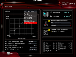
All eight fan headers can be switched from PWM to voltage mode as needed, or left to detect the appropriate mode on their own. Users can select from one of the factory speed profiles, or define their own. And one of those headers is even specified to support up to 3A loads.

A simplified version of RGB Fusion is found on the firmware GUI’s “Peripherals” menu, where users who don’t need as many settings can make lighting scheme changes without the need for additional software.


Switching to “Easy Mode” from the lower screen popup of Classic Mode gets users to a safe place where they can’t overclock, but can still enable auto-overclocking, XMP mode for faster memory, alter boot order, and access the “Smart Fan 5” menu described previously. Unfortunately, the overclocking profile chosen by firmware was designed for a Core i3-8350K operating at only 4.20 GHz.
MORE: Best Motherboards
MORE: How To Choose A Motherboard
MORE: All Motherboard Content
Stay on the Cutting Edge
Join the experts who read Tom's Hardware for the inside track on enthusiast PC tech news — and have for over 25 years. We'll send breaking news and in-depth reviews of CPUs, GPUs, AI, maker hardware and more straight to your inbox.
-
sp5618 First-time PC builder does this board have a thunderbolt 3rd generation 40 MB? If not what motherboards in the ATX form factor Have it? Thank youReply -
Crashman Reply
Leave it empty?20951510 said:I don't know what to do with the third M2 slot
Chipset limitations are butting up against the desire to extend M.2 support: These companies want a third x16 slot with four lanes, and at least two NVMe M.2 slots, but that combination uses 12 of the 30 HSIO ports. Gigabyte added another NVMe M.2 slot that kills off a couple SATA lanes when its being used, I guess they could have just left off that M.2 slot, knocked the SATA port count down to four, and included a fully-utilized Thunderbolt controller instead.20951647 said:First-time PC builder does this board have a thunderbolt 3rd generation 40 MB? If not what motherboards in the ATX form factor Have it? Thank you
Nearly all of these boards are designed to host a Thunderbolt add-in card in the four-lane slot, but most of those slots require you to sacrifice some other interface. Look for the Thunderbolt add-in-card header.
On the other hand, Mini ITX has fewer slots, and several of those boards have Thunderbolt controllers to use up some of the leftover HSIO.
-
Crashman Reply
I realize that Gigabyte is using split-phase design. I've always hated counting phases because the number hasn't meant anything since companies came out with 24 low-amperage phases to compete with the six to twelve high-current phases of competitors back in the Core 2 days. I only include the easiest number because so many people don't understand what i just said.20951814 said:1 inductor does not equal 1 phase
-
android_dev It's a 8+3 phase with the voltage controller being a true 4 phase on the CPU section doubled to 8 with additional mosfet drivers while the other 3 are for iGPU.Reply -
Crashman Reply
I thought the other three were for the entire system agent, including the memory controller :)20976842 said:It's a 8+3 phase with the voltage controller being a true 4 phase on the CPU section doubled to 8 with additional mosfet drivers while the other 3 are for iGPU. -
android_dev Reply20976876 said:
I thought the other three were for the entire system agent, including the memory controller :)20976842 said:It's a 8+3 phase with the voltage controller being a true 4 phase on the CPU section doubled to 8 with additional mosfet drivers while the other 3 are for iGPU.
It's another voltage controller that controls the memory VRM which is a Richtek RT8120. The CPU Core Voltage VRM uses an Intersil 95866 which is a true 4+3 phase which Gigabyte has doubled to 8+3 phase. System Agent and VCCIO use Richtek RT8120D which is 1 phase each.
-
Crashman Reply
I didn't mention the memory signal voltage controller, for which the components can usually be seen separated from the group of things for various CPU devices ;)20976914 said:20976876 said:
I thought the other three were for the entire system agent, including the memory controller :)20976842 said:It's a 8+3 phase with the voltage controller being a true 4 phase on the CPU section doubled to 8 with additional mosfet drivers while the other 3 are for iGPU.
It's another voltage controller that controls the memory VRM which is a Richtek RT8120. The CPU Core Voltage VRM uses an Intersil 95866 which is a true 4+3 phase which Gigabyte has doubled to 8+3 phase. System Agent and VCCIO use Richtek RT8120D which is 1 phase each.
As for the 4/8, I say split, you say doubled. But getting back to the original message, we were seeing 24+ voltage regulators on P35/P45 boards before someone else (I think MSI) came out with higher capacity parts on a 6-phase design that could do the same work at lower cost. Soon after we were frying 12 phase regulator components and not frying 8 phase components when doing the same thing, because the boards with the 12 phase regulators were using substandard parts. Then some companies put high-amp chokes on low-amp MOSFETs and I blew more boards.Then some companies put high-amp chokes AND MOSFETs on the same board and extreme overclockers blew traces surrounding the MOSFETs. Then some companies used a thicker copper layer on the PCB with higher amp parts and hollow EPS12V pins and I blew out the connector. We even had sockets without enough contact pressure on the pins blowing out. Because of this, the only way I can find the weak point is through testing. And because of that, I'm now treating "phase count" as a matter of trivia.
-
android_dev Reply20977076 said:
I didn't mention the memory signal voltage controller, for which the components can usually be seen separated from the group of things for various CPU devices ;)20976914 said:20976876 said:
I thought the other three were for the entire system agent, including the memory controller :)20976842 said:It's a 8+3 phase with the voltage controller being a true 4 phase on the CPU section doubled to 8 with additional mosfet drivers while the other 3 are for iGPU.
It's another voltage controller that controls the memory VRM which is a Richtek RT8120. The CPU Core Voltage VRM uses an Intersil 95866 which is a true 4+3 phase which Gigabyte has doubled to 8+3 phase. System Agent and VCCIO use Richtek RT8120D which is 1 phase each.
As for the 4/8, I say split, you say doubled. But getting back to the original message, we were seeing 24+ voltage regulators on P35/P45 boards before someone else (I think MSI) came out with higher capacity parts on a 6-phase design that could do the same work at lower cost. Soon after we were frying 12 phase regulator components and not frying 8 phase components when doing the same thing, because the boards with the 12 phase regulators were using substandard parts. Then some companies put high-amp chokes on low-amp MOSFETs and I blew more boards.Then some companies put high-amp chokes AND MOSFETs on the same board and extreme overclockers blew traces surrounding the MOSFETs. Then some companies used a thicker copper layer on the PCB with higher amp parts and hollow EPS12V pins and I blew out the connector. We even had sockets without enough contact pressure on the pins blowing out. Because of this, the only way I can find the weak point is through testing. And because of that, I'm now treating "phase count" as a matter of trivia.
Hmm.. interesting, I was too young back then when you reviewed that stuff 10+ years ago now but yeah I read circuit analysis reviews of this motherboard and that's how I got the info for what I wrote above.
