Semiconductor Production 101
Etch And Strip
The wafer now enters a so-called developer process during which remove the weakened photoresist is removed, which helps to transfer patterns onto the silicon dioxide. There are wet and dry etch processes that treat the exposed silicon dioxide; wet processes use chemical substances and dry processes use gases. The removal of the remaining photoresist is called strip. Manufacturers often combine dry and wet strippers to make sure that the photoresist is completely removed. This step is important as photoresists are organic materials, which, if not properly removed, cause defects on the wafer. After etching and stripping, a wafer can either be inspected (which typically is the case after almost every major step), or it can go directly into a new photolithography cycle.
Wafer Test, Assembly, Packaging
Wafer Test
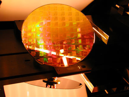
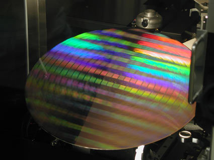
Completed wafers are tested by putting them onto so-called wafer probers. They handle the complete wafer, align them and create contacts to a probe card, so each contact for each die can be connected electrically. Under software control, all features of each die are tested.
Get Tom's Hardware's best news and in-depth reviews, straight to your inbox.
Tom's Hardware is the leading destination for hardcore computer enthusiasts. We cover everything from processors to 3D printers, single-board computers, SSDs and high-end gaming rigs, empowering readers to make the most of the tech they love, keep up on the latest developments and buy the right gear. Our staff has more than 100 years of combined experience covering news, solving tech problems and reviewing components and systems.


