Semiconductor Production 101
Photolithography
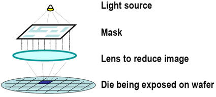
Lithography is the process used to apply patterns onto a silicon wafer. The process is typically repeated several times, until multiple layers (20+) are created. These layers can consist of different materials, and all of them are interconnected (wired) very specifically. All of them can also be doped.
Before the photolithographic process can begin, the wafer is cleaned and heated up to remove adhesive particles and water. This is called pre-bake. Then the wafer is coated with silicon dioxide, using a device that is called coater. An adhesive agent is applied to the wafer to make sure that the photoresist (also called resist), which is applied in the following step, will abide on the wafer. The photoresist is applied to the middle of the wafer, which is then rotated at a high revolution speed to apply an even layer across the entire wafer surface. The wafer is heated up again, which is called post bake.
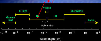
Excimer lasers, extreme ultraviolet light, x-rays, electron beams or ion beams are the possible light or energy source that are used to expose surfaces through or without the reticle/mask. Electron beams are primarily used to create the masks, while x-ray and ion beams are used for research purposes, making EUV light and gas lasers the dominating light sources today.
EUV lights with a wave length of 13.5 nm are used to expose the photoresist and transfer images from masks to the silicon wafer.
The exposure time and focus are very important to reach the desired results. An inadequate focus will result in leftover photoresist particles as some holes aren't exposed properly. You get similar results with underexposure. The photoresist webs can easily be too wide and holes aren't exposed sufficiently. Overexposure creates holes that are too large or photoresist webs that are too thin. It's tricky and time-consuming to adjust and optimize this process, and inappropriate holes will hamper the interconnects.
So called steppers are used to move the wafer to the exact position. A row or a different section, typically a single die, can then be exposed properly. So-called micro steppers or micro exposure tools can then be used to make additional changes. This is used to debug existing technology and optimize the production process. Micro steppers usually work at areas of less than 1 mm, while regular steppers cover much larger areas.
Get Tom's Hardware's best news and in-depth reviews, straight to your inbox.
Tom's Hardware is the leading destination for hardcore computer enthusiasts. We cover everything from processors to 3D printers, single-board computers, SSDs and high-end gaming rigs, empowering readers to make the most of the tech they love, keep up on the latest developments and buy the right gear. Our staff has more than 100 years of combined experience covering news, solving tech problems and reviewing components and systems.


