
Intel has started volume production of its Core Ultra 3-series 'Panther Lake' processors, the company said on Thursday. Intel's Panther Lake is a crucial CPU for the company, designed to demonstrate Intel's ability to develop a competitive processor and produce it internally using its leading-edge manufacturing technology. This is intended to enhance the company's reputation among clients, the general public, and potential foundry customers.
While the official start of 18A production is a win for the company, as it is technically the first with a 2nm-class node in production, it still faces a potent foe in TSMC — the new node merely represents catching up rather than taking the lead. Here's how the two nodes stack up.
Intel 18A vs. TSMC's N2
Intel's 18A (1.8 nm-class) fabrication process is one of the key features of the company's next-generation Panther Lake platform, serving as both its technological showcase and strategic milestone.
Article continues below


The 18A production node itself is designed to prove that Intel can not only create a compelling CPU architecture but also manufacture it internally on a technology node competitive with TSMC's best offerings. The node is also the first 1.8 nm-class (or, as Intel brands it, 2 nm-class) process to enter high-volume production anywhere in the world, preceding TSMC's N2 by weeks or even months.
18A employs Intel's RibbonFET gate-all-around transistors and PowerVia backside power delivery, two technological breakthroughs implemented simultaneously. Intel de-risked these two innovations separately in different internal nodes, but implementing them simultaneously for the first time in a production node is still a somewhat risky move intended to demonstrate that Intel can leap forward and introduce these innovations at once.
| Row 0 - Cell 0 | Intel 18A vs Intel 3 | N3P vs N3E | N2 vs N3E | N2P vs N3E | N2P vs N2 | A16 vs N2P | N2X vs N2P | A14 vs N2 | A14 SPR vs N2 |
Power | -25% | -5% ~ -10% | -25% ~ -30% | -36% | -5% ~ -10% | -15% ~ -20% | lower | -25% ~ -30% | lower |
Performance | 15% | 5% | 10% - 15% | -18% | 5% - 10% | 8% - 10% | 10% | 10% - 15% | higher |
Relative Transistor Density* | 1.3X | 1.04X | 1.15X | higher | ? | 1.07x - 1.10x | ? | 1.2x | denser |
Transistor Density | 238 MTr/mm^2 (HD)** | 180 - 220 MTr/mm^2*** | 313 MTr/mm^2 (HD)** | higher | higher | ? | ? | ? | very high |
Transistor Type | GAA | FinFET | GAA | GAA | GAA | GAA | GAA | 2nd Gen GAA | 2nd Gen GAA |
Power Delivery | PowerVia BSPDN | SHDMIM | Front-side w/ SHPMIM | Front-side w/ SHPMIM | Front-side w/ SHPMIM | SPR | Front-side w/ SHPMIM (?) | Front-side w/ SHPMIM (?) | SPR |
HVM | Q4 2025 | Q4 2024 | Q4 2025 | H2 2026 | H2 2026 | H2 2026 | 2027 | 2028 | 2029 |
*Chip density published by TSMC reflects 'mixed' chip density consisting of 50% logic, 30% SRAM, and 20% analog.
**According to TechInsights.
*** According to WikiChip.
Analysts believe that Intel's 18A will lead the industry in terms of performance and power efficiency. However, TSMC's N2 is projected to offer considerably higher high-density (HD) standard-cell transistor density (313 MTr/mm^2) compared to Intel's 18A (238 MTr/mm^2), according to reports.
While most modern designs use a mix of high-density (HD), high-performance (HP), and low-power (LP) standard cells, higher HD transistor density could still mean lower per-transistor costs for the foundry. However, it is unclear whether these savings will be passed on to the company's clients.
Furthermore, it should be noted that when comparing the transistor density of Intel's 18A, which features a backside power delivery network, with TSMC's N2, which uses a traditional frontside PDN, the comparison is not entirely accurate. Intel's 18A leaves the front side almost entirely for signal interconnects and logic transistors, whereas TSMC's N2 uses plenty of transistors on the front side for power distribution (power-gating header/footer switches, ESD, MOS decaps, on-die regulators, etc.). As a result, 18A's and N2's effective transistor densities could be very close.
However, flipping the wafer and producing a power delivery network on the backside costs money, so Intel's 18A is likely a more expensive process technology to fabricate than TSMC's N2, which will not be a problem for premium products, though.
While 18A looks good in general on paper, the competitiveness of Intel's Core Ultra 3 'Panther Lake' and Xeon 6+ 'Clearwater Forest' is an important step for Intel toward regaining manufacturing credibility and attracting external foundry customers for 18A, 18A-P, and future 14A nodes.
Production slip and Intel 18A yields
Intel says Panther Lake's compute tiles on 18A 'began early production' at its development and low-volume fabs in Oregon, and 'is now ramping toward high-volume production in Arizona.' As expected, Intel first began to ramp Panther Lake manufacturing at Fab 52. Apparently, Fab 62 is still under construction and will be ramped up when demand for 18A picks up.
The first Panther Lake CPU model is 'slated to ship before the end of the year and broad market availability starting January 2026.' Such an announcement signals a delay, as originally Intel indicated the availability of Panther Lake processors in 2025. Furthermore, the announcement may also highlight a slower-than-expected volume ramp, as the company previously indicated that additional Panther Lake models (not just the halo SKU) would be rolled out in the first quarter of 2026. This time around, Intel didn't reveal when it expects the whole Panther Lake product lineup to ramp up.
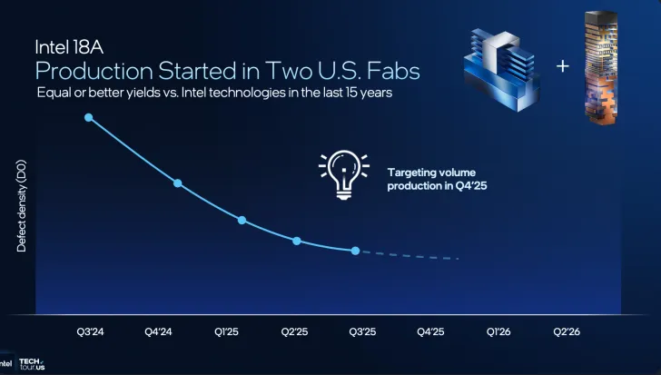
The delay of Intel's Panther Lake launch and the slower ramp of its 18A process may suggest that the node may have yield, performance variability, or packaging challenges. However, Intel presented a defect density (D0) graph showing their consistent decrease. Taking a page from some of its rivals, Intel did not mark the Y-axis of the graph, so all we know is that 18A's defect density decreased from 0.4 defects per square centimeter in Q3 2024 to somewhere below that figure in Q3 2025.
While D0 is an important metric, it does not significantly relate to parametric yields, which define whether a chip achieves its desired performance and power targets. For example, a chip can be defect-free but still fail to meet performance or power targets due to a narrow process window, systematic or random critical dimension (CD) variations, stochastic line-edge roughness (LER) variations, transistor mismatch, or marginal design corners.
Intel stresses that 18A yields (we presume, the yields of Panther Lake's compute tile) are equal or better than those of chips produced on previous-generation nodes in the last 15 years, though it is logical that a relatively small compute tile of Panther Lake (100 – 110 mm^2) has higher functional yield of rather big monolithic CPUs from 2012 – 2018 (122 mm^2 – 160 mm^2 ) and large monolithic CPUs from 2018 – 2022 (180 mm^2 – 276 mm^2).
Anyway, despite an earlier delay, Intel's 288-core Xeon 6+ 'Clearwater Forest' data center is still on track for launch in the first half of 2026, which suggests that the issues (if there are issues) are identified and are on track to be solved in the next nine months.
Strategically, even though some may argue Intel 18A was successful due to Intel's goalposts being defined as when the node was 'production ready' as opposed to when it began production, the delay weakens Intel’s credibility in its 'five nodes in four years' roadmap and diminishes its opportunity to leap ahead of TSMC's N2, which is expected to enter high-volume production in Q4 2025 and ramp numerous client and data center products in the first half of 2026. As a result, instead of a clear process leadership win, Intel risks being perceived as merely catching up.
Follow Tom's Hardware on Google News, or add us as a preferred source, to get our up-to-date news, analysis, and reviews in your feeds. Make sure to click the Follow button!
