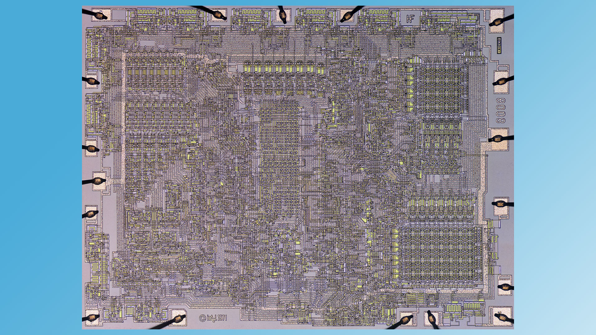
CPU collector stitches 216 micrographs to create high resolution die shot of the legendary i8008 — Intel’s 54-year-old milestone 8-bit CPU seen like never before
Super sharp imagery reveals the structure of this milestone CPU from Intel.

A CPU collector has shared some fantastically detailed new images of the landmark Intel 8008 processor. CPU Duke seriously indulged their CPU microscopy hobby over recent days, creating a detailed die-shot of an i8008 by carefully aligning and stitching 216 individual micrographs.
In a thread, CPU Duke explains that the chip under close scrutiny was kindly donated by a computer museum called the ENTER Technikwelt in Solothurn, Switzerland. The donation apparently came with a request that CPU Duke create some die shots of the early 1970s CPU.
It’s the 8008, the first #8bit CPU of #Intel…I stitched 216 individual #microscopy pictures to get this high resolution canvas of the die from 1971.(8/n) https://t.co/nci4JmoB0S pic.twitter.com/lKihf7qL9MOctober 20, 2025
Importance of the Intel 8008
The Intel 8008 was a milestone development as the chipmaker’s first 8-bit microprocessor. It was designed in 1971 by more or less the same team behind the i4004, with the new i8008 chip being released in April 1972. This sample was fabricated on the 10 micron PMOS process in Barbados. CPU Duke confirmed that this CPU was indeed manufactured in the Caribbean island nation, where Intel ran an assembly plant until 1986.
Creating the die shot image
The process behind creating a die shot of a chip like this begins with a little silicon torture. CPU Duke shows the exact moment they ‘decapped’ the CPU here (animated GIF alert) with a screwdriver blade. Ahead of that, they stretched out the CPU’s DIP IC pins to fit in a press, then heated the processor package to around 600 degrees Celsius. With the silicon exposed, it was time to get the imaging equipment ready.
#Halloween time is decapping time! 🎃 Of course no humans or animals were harmed in the process…only a long forgotten #IntegratedCircuit revealing a precious 8bit #die…more soon to come. 💀 pic.twitter.com/asZf1N8RXgOctober 15, 2025
The first imaging step was to take a few macrographs, for a good overview of what was revealed by decapping. Next, the CPU collector reveals that a more detailed survey of the i8008 was created using a “Wild/Leica stereomicroscope with phototube.” Later, the CPU enthusiast got much much closer to create the final image (embedded top), which required the painstaking alignment and stitching of 216 individual micrographs from CPU Duke’s equipment.
What the CPU die shot shows
Without getting too close, some details of the i8008 are already quite clear. Even with the naked eye, you can see the 18-pin bond pad connectors that interface the chip and socket. Also easily visible are markings showing ‘Intel 1971’, ‘8008’, and ‘HF’. That pair of initials is thought to pay tribute to the newest member of the i8008 design team, Hal Freeny. Freeny joined the i4004 team to design this 8-bit CPU.
CPU Duke comments that the 10 micron PMOS structure is actually so coarse that “light microscopy is still feasible.” Zooming closer, the CPU collector notes the visibility of the p-channel MOS structure under the metal surface. Specifically, semiconducting polysilicon is dark green, non-conducting bright green in some of the light microscopy shots shared.
Get Tom's Hardware's best news and in-depth reviews, straight to your inbox.
The final stitched micrograph might have been more illuminating had it been color-coded with some kind of overlay. However, computer historian and reverse engineer Ken Shirriff has already shared an overview analysis of the 8008 die. Thus, you can cross-reference that coarser imagery to determine which areas of this fresh new die shot are devoted to the ALU, registers, stack counter, data bus, and so on.

Follow Tom's Hardware on Google News, or add us as a preferred source, to get our latest news, analysis, & reviews in your feeds.

Mark Tyson is a news editor at Tom's Hardware. He enjoys covering the full breadth of PC tech; from business and semiconductor design to products approaching the edge of reason.