Intel Architecture Day 2021: Alder Lake Chips, Golden Cove and Gracemont Cores
Alder Lake Comes to Fore
Intel's mission with the efficiency core (E-Core), which is based off the Atom Gracemont architecture (though Intel has dispensed with the 'Atom' branding) was to create a highly scalable architecture optimized for multi-core performance-per-watt. The engineers set an aggressive silicon area target, meaning they aimed to pack as many cores with as much performance as possible into a small footprint, and set out to deliver more IPC than Skylake within a lower power envelope. We'll jump ahead here and show you Intel's claimed results, and then show you how Intel got there. As with all vendor-provided benchmarks, view these with the appropriate skepticism.
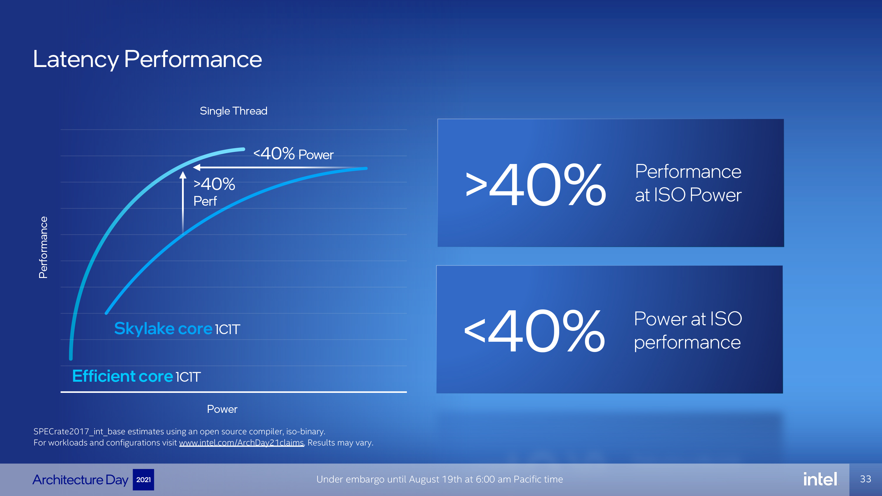
The latency performance chart, which quantifies single-threaded performance, is first up. First, be aware that Intel tested with the SPECrate2017_int_base test for these results, meaning the test represents performance with integer workloads, not floating point. For the single-threaded test, Intel disabled hyperthreading on an undisclosed Skylake processor (likely first gen) and measured performance against a single Gracemont core, which doesn't support hyper-threading. That means we're looking at a pure single-core benchmark for both processors. Gracemont provided 40% (or more) performance at the same power (ISO power) as the Skylake chip, or provided the same level of performance (ISO performance) at less than 40% of the power. That means that the Skylake core consumed 2.5 times more power to give the same level of performance as the Gracemont core.
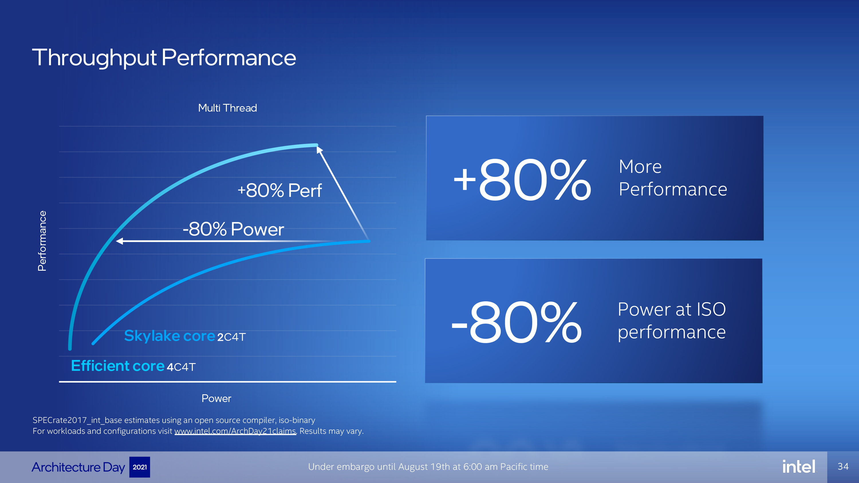
The throughput performance test measures performance spread over multiple threads, with four single-thread Gracemont cores facing off with two threaded Skylake cores (for a total of four threads). Here Gracemont delivers 80% more performance while consuming less power, or the same throughput at 80% less power. That means Skylake needed five times the power for the same performance in threaded work, which is impressive indeed.
It's worth nothing that threading tends to only deliver about ~20-30% more performance, so the Skylake chip is at a disadvantage, though it only pays about a 5% penalty in die area to add threading. To even this out, consider that the four Gracemont cores fit into the same footprint as a single Skylake core, meaning that Gracemont not only wins on all counts in these integer workloads, but its area efficiency is vastly superior. Net net, according to Inntel, Gracemont exceeds Skylake's core performance while consuming less power in a far smaller footprint. Here's how they did it.
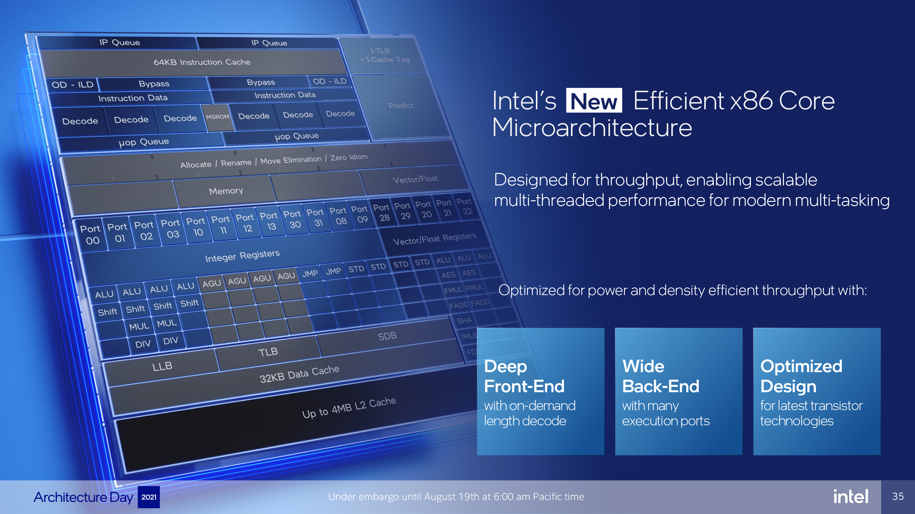
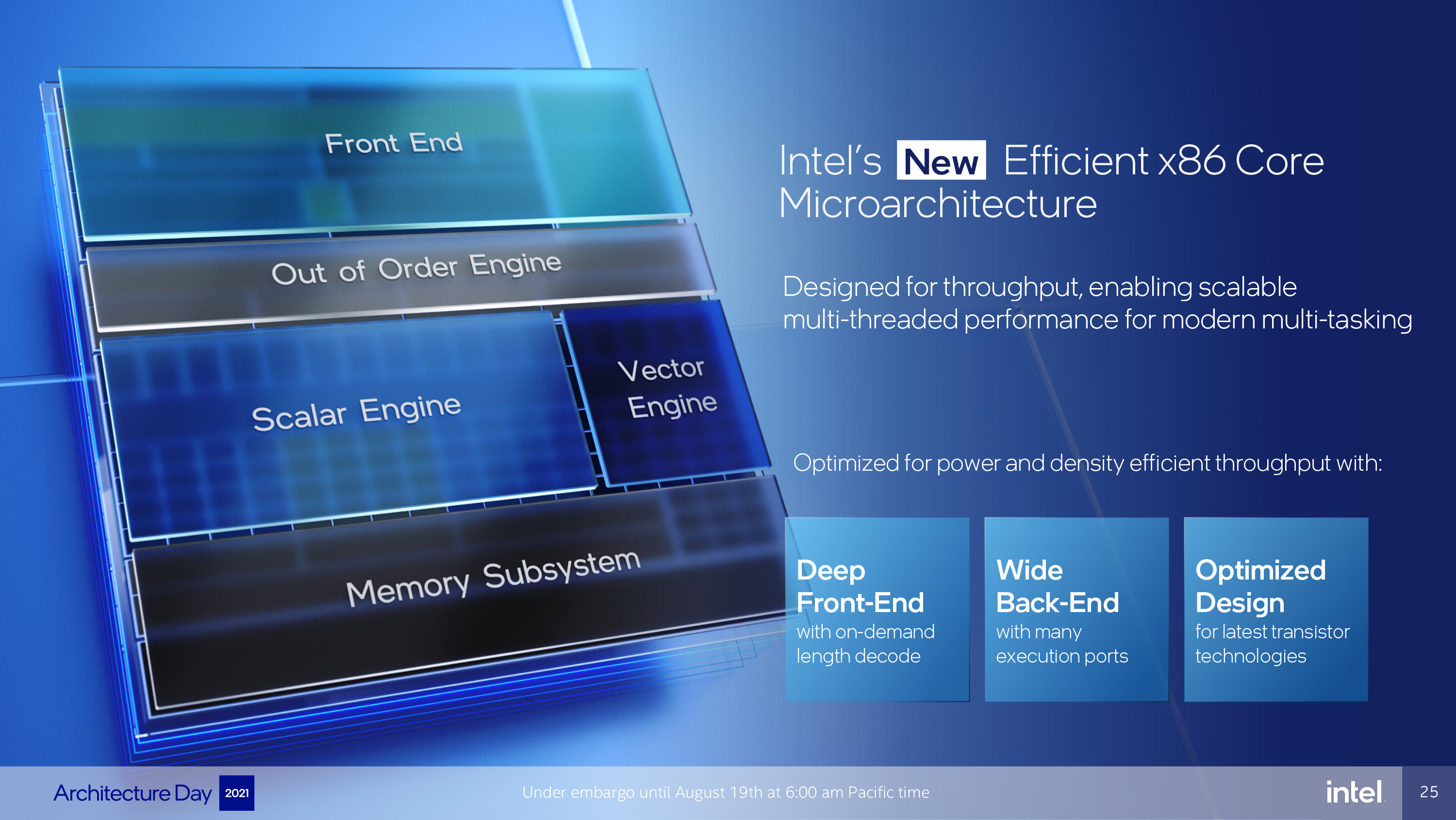

From the highest of levels, Intel designed Gracemont with a deeper front end with on-demand length decode paired with a wider back end with more execution ports. The design supports vector and AI instructions, like VNNI and AVX-256, but doesn't support AVX-512. Additionally, Intel aimed for a wide dynamic frequency range to maximize the effective range of the processor.
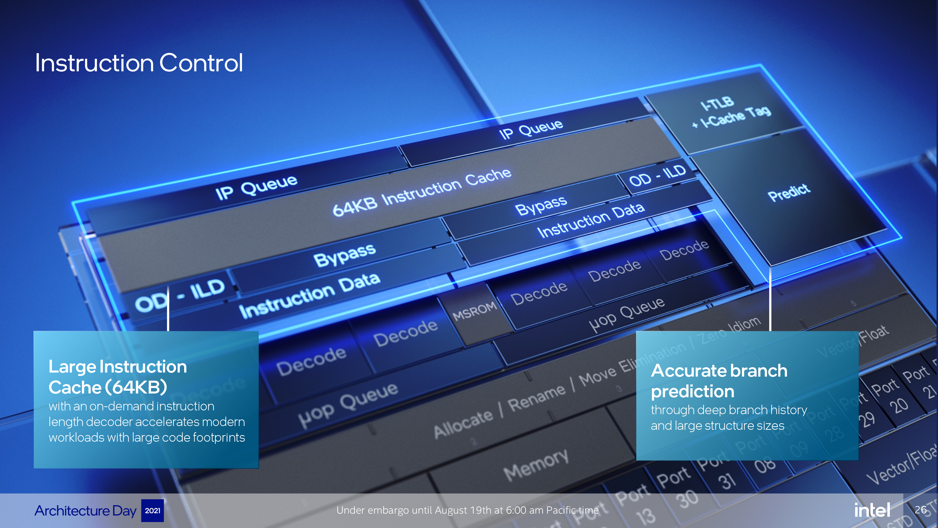
Intel increased branch prediction accuracy by switching to a 5,000-entry branch target cache. Additionally, Intel says its new 'long' history-based branch prediction system helps to generate accurate instruction pointers, which then allows discovery and correction of instruction cache misses before they become critical to program execution. The front end also has a 64KB instruction cache to keep instructions close, thus saving power. The chips also have Intel's first on-demand instruction length decoder, which generates pre-decode information that is then stored alongside the instruction cache. This provides a history of previous instructions that allows 'familiar' code to bypass the length decoder to save energy.
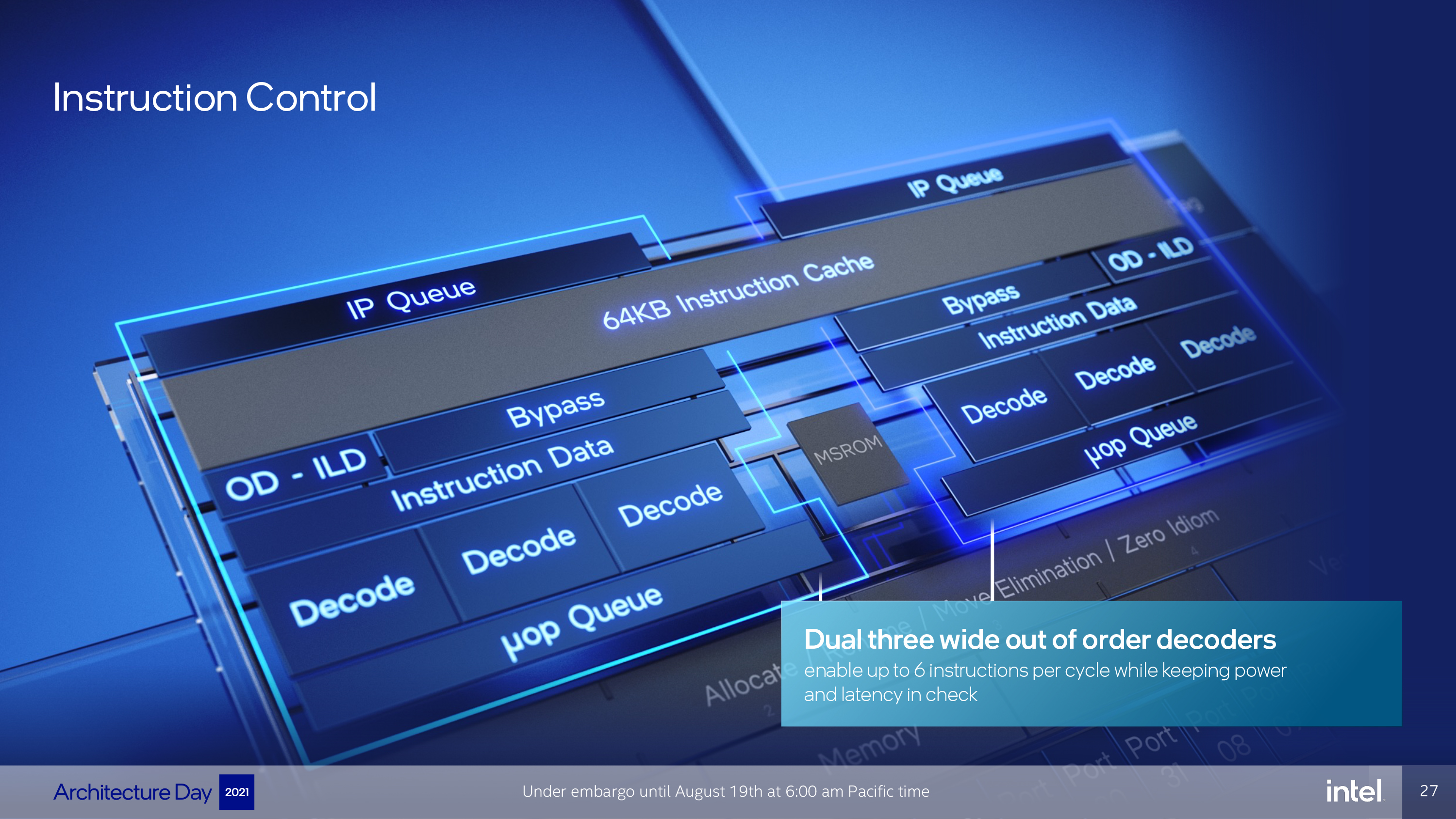
The out-of-order decoder has a clustered design with dual three-wide decoders. This allows for decoding up to six instructions per cycle while, according to Intel, maintaining comparable energy efficiency to a narrower design. The unit also has hardware-driven load balancing to ensure parallelism.
Get Tom's Hardware's best news and in-depth reviews, straight to your inbox.
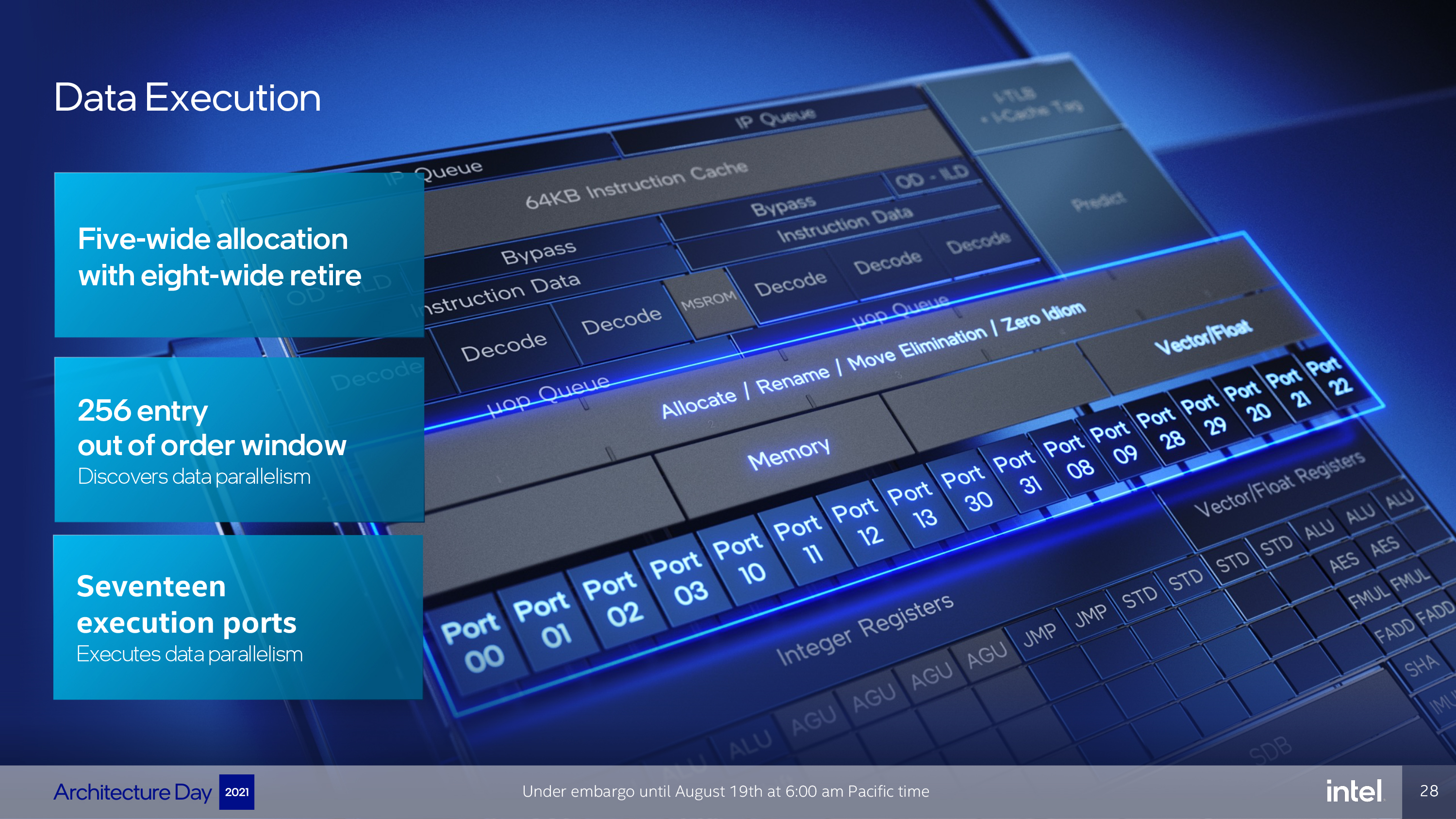
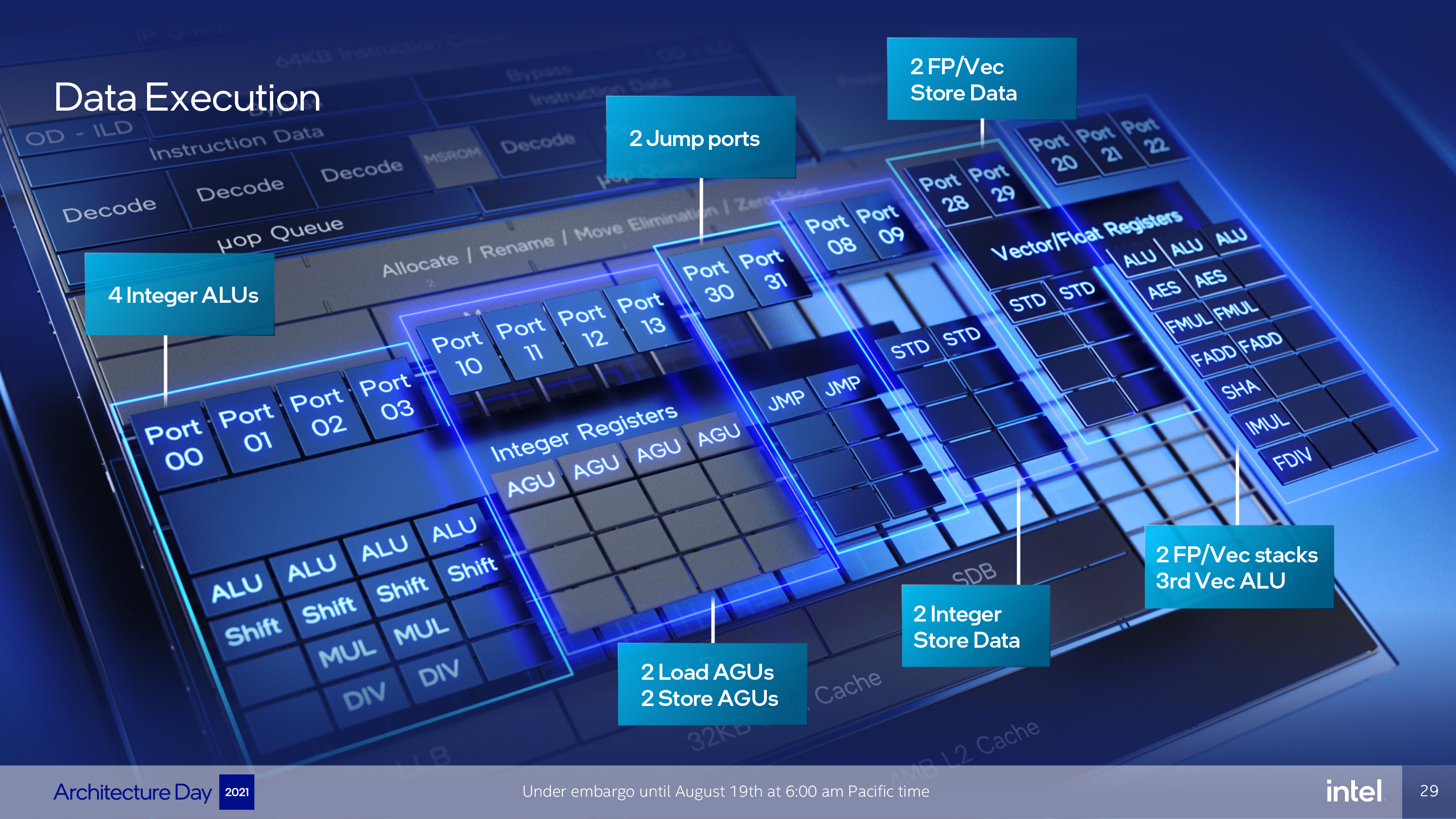
The back end has a five-wide allocation and eight-wide retire, along with a 256 entry out-of-order window that helps to promote parallelism. That's fed to 17 execution ports. Intel says this arrangement delivers more integer IPC than Skylake, but at a fraction of the power.
There are four general-purpose integer execution ports with dual integer multipliers and dividers that can resolve two branches per cycle. To the far right we can see the three SIMD ALUs with the integer multiplier (IMUL) that's used for Intel's VNNI instructions. The two symmetric floating point pipelines can do two independent add or multiply operations, and can also do two FP multiply/add operations per cycle via vector extensions. We can also see the AES and SHA acceleration engines in the same stack.
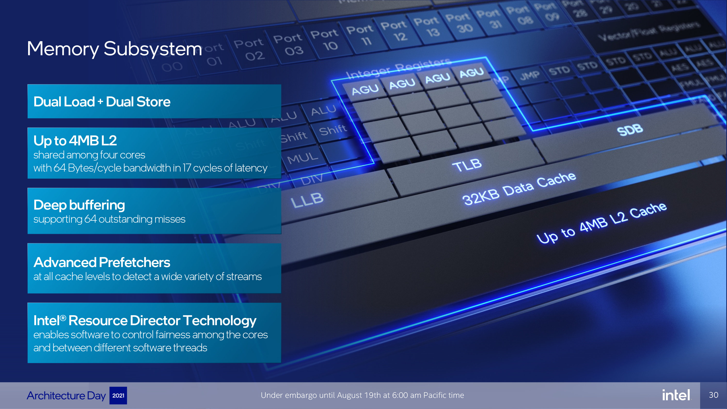
Moving down to the memory subsystem, we can see dual load and dual store pipelines that support 32KB read and write bandwidth simultaneously. The L2 cache is shared among all four cores, with 2MB for consumer chips and 4MB for data center models. This feeds the cores with 64 bytes of read bandwidth per cycle at 17 cycles of latency.
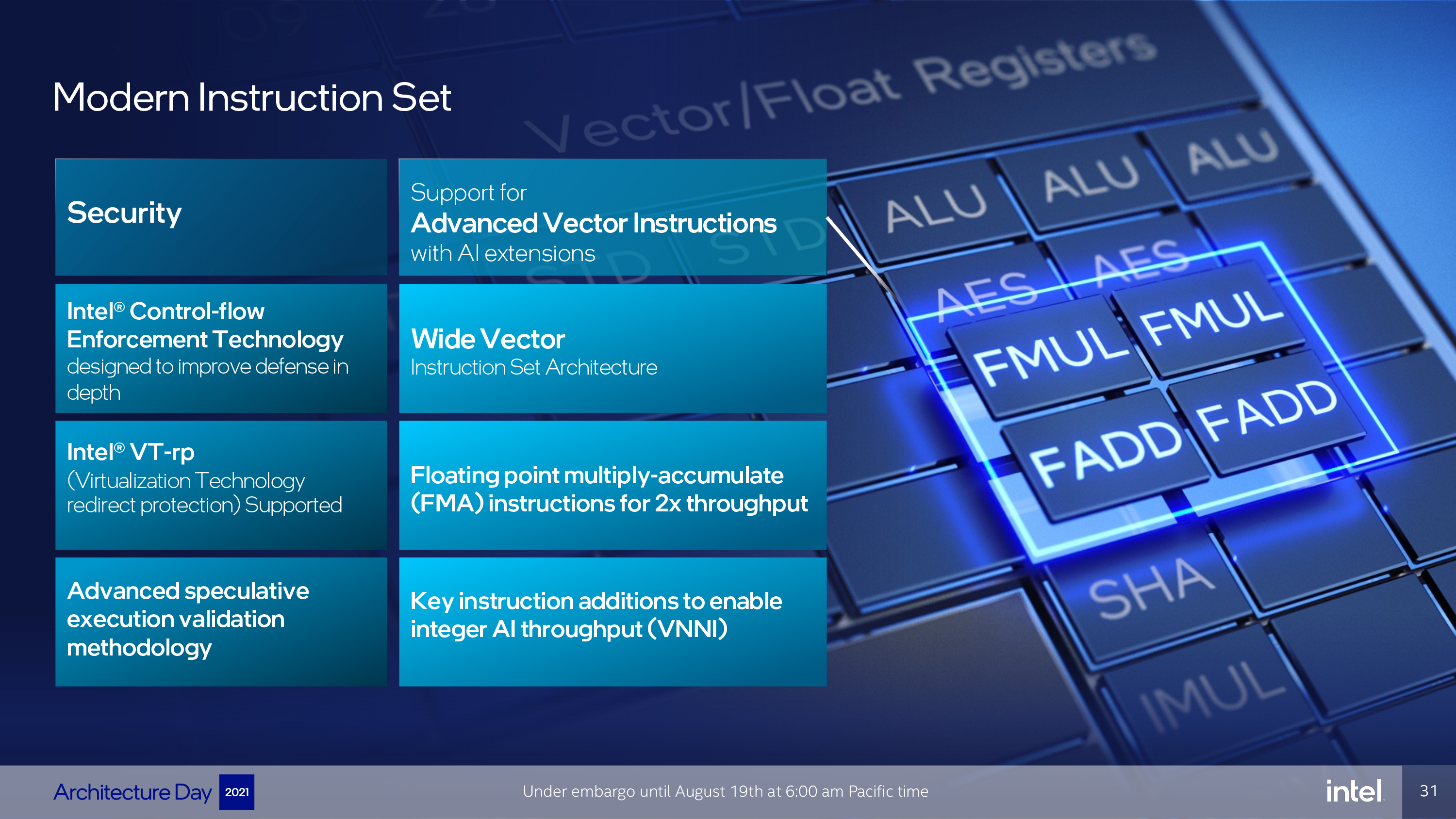
Intel also touts Alder's modern instruction set with Control-flow Enforcement Technology (CET), VT-rp, support for vector instructions (up to AVX-512), and AVX2 VNNI, which uses FP16 instructions to impart a 2X performance gain in integer AI throughput.
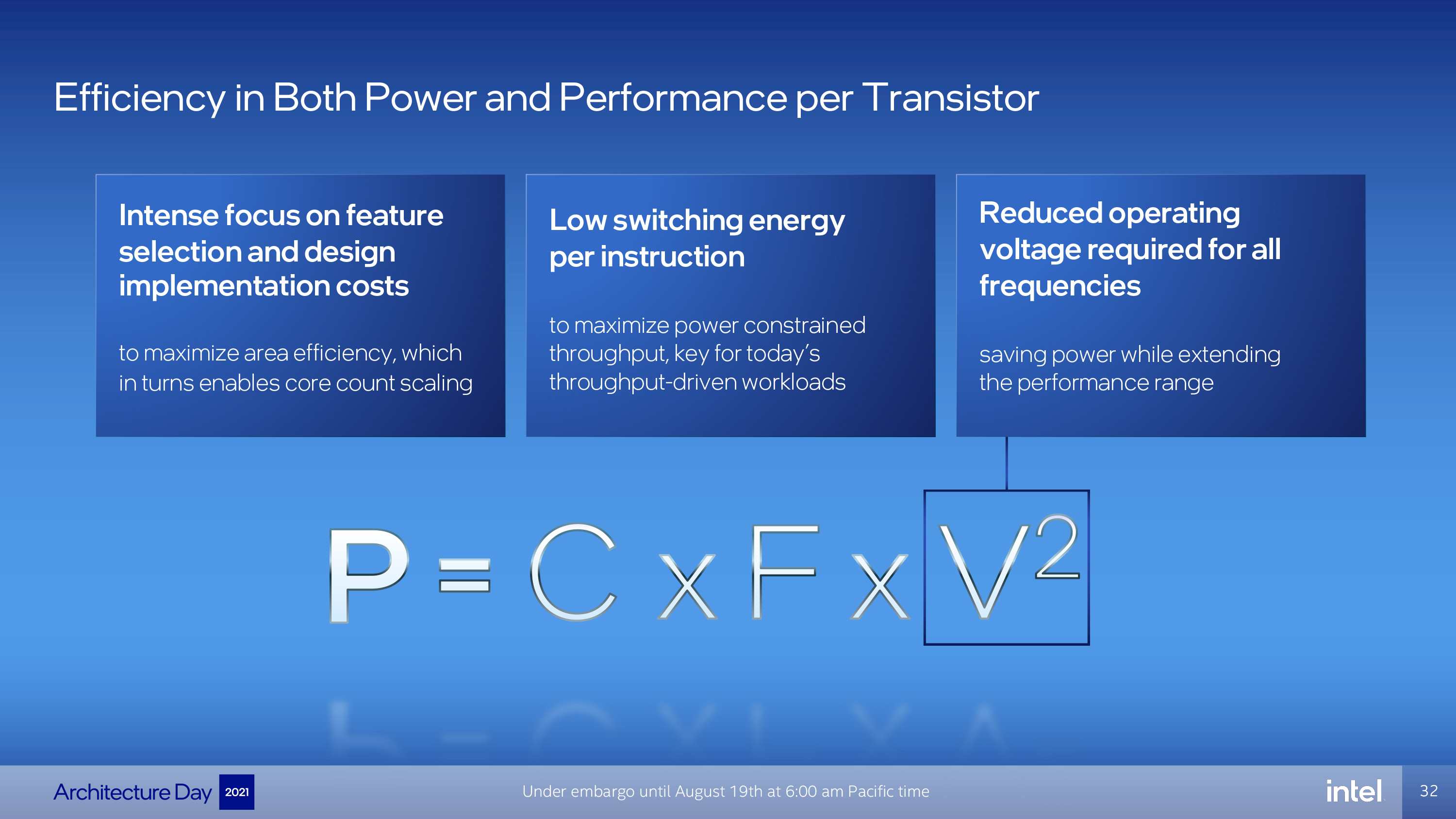
Gracemont's focus on area efficiency allows Intel to, for a lack of a better term, spam cores. Intel can essentially just drop in lots of four-core clusters to pack a lot of compute into a very small area and the low switching energy per instruction maximizes power-constrained throughput in heavily-threaded workloads. This is enabled by a reduced operating voltage that not only saves power (voltage is the most important factor here), but also provides headroom for higher frequencies for on-demand peak performance.
Current page: Intel Alder Lake Gracemont Efficiency Core
Prev Page Intel Alder Lake Thread Director Technology and AVX-512 Next Page Intel Alder Lake Golden Cove Performance Core
Paul Alcorn is the Editor-in-Chief for Tom's Hardware US. He also writes news and reviews on CPUs, storage, and enterprise hardware.
-
TerryLaze ReplyAlder Lake does not support AVX-512 under any condition (fused off in P cores, not supported in E cores).
Called it that all they need to do to get power draw down to ryzen levels is to turn off avx.
If they also locked down power limits, at least on non OC boards, they can sell it as super future low power tech. -
JWNoctis No AVX-512 at all?...Yeah, that's gonna be a rather huge regression for those applications that made use of them, which is admittedly uncommon in consumer space.Reply
But then there's not that much difference between Core, Pentium, and Celeron lines anymore, unless they are going to detune IPC in microcode or something. What's the name of the next one, I wonder? -
TerryLaze Reply
Rocketlake didn't get any pentiums or celerons, no reason to believe that alder lake will have them.JWNoctis said:No AVX-512 at all?...Yeah, that's gonna be a rather huge regression for those applications that made use of them, which is admittedly uncommon in consumer space.
But then there's not that much difference between Core, Pentium, and Celeron lines anymore, unless they are going to detune IPC in microcode or something. What's the name of the next one, I wonder?
Now the celeron (atom) is going to be integrated in the core... :p -
Giroro Intel keeps talking up how great their tiny gracemont cores are... But if 4 gracemont cores were able to outperform 1 Golden Cove core, then the entire CPU would be gracemont. I think its no coincidence that their desktop CPUs tacked on exactly enough tiny cores to confuse people into thinking they have parity with 16-core ryzen. Just like how they renamed their 10nm process to give the illusion of parity.Reply
I have no confidence whatsoever that their 8C/8c/24t processor has better multithreaded performance than a hypothetical 10C/0c/20t processor. If that were the case, then the configurations would be more like 0C/40c/40t... Or maybe even 2C/32c/36t.
But no, this is all about how they can technically get away with selling what is essentially an 8 core processor, using a giant sign that says 16 CORES* WORLD'S BEST EFFICIENCY**!
They at least know performance matters a little bit, because a 40 CORE CPU has to got be pretty tempting to somebody in their marketing department, regardless of how bad it would be. -
Johnpombrio This will probably be my next CPU replacing my i9-9900K. I need at least PCI-4.0 for my 2TB Samsung 980 Pro ($313 lightning deal in Amazon Prime day in June). I will never need all of these cores tho.Reply -
mdd1963 Cautiously optimistic, but, I recall feeling the same way before 11th gen released...Reply
This time I will be pessimistic until happily (hopefully) proven wrong. :)
(Need some BF1/BF5 1080P benchmarks to truly know if Alder Lake is 'mo betta'!) -
JamesJones44 ReplyGiroro said:Intel keeps talking up how great their tiny gracemont cores are... But if 4 gracemont cores were able to outperform 1 Golden Cove core, then the entire CPU would be gracemont. I think its no coincidence that their desktop CPUs tacked on exactly enough tiny cores to confuse people into thinking they have parity with 16-core ryzen. Just like how they renamed their 10nm process to give the illusion of parity.
I have no confidence whatsoever that their 8C/8c/24t processor has better multithreaded performance than a hypothetical 10C/0c/20t processor. If that were the case, then the configurations would be more like 0C/40c/40t... Or maybe even 2C/32c/36t.
But no, this is all about how they can technically get away with selling what is essentially an 8 core processor, using a giant sign that says 16 CORES* WORLD'S BEST EFFICIENCY**!
They at least know performance matters a little bit, because a 40 CORE CPU has to got be pretty tempting to somebody in their marketing department, regardless of how bad it would be.
How do you explain M1s multi thread performance then, the quote makes little sense. There is a lot more to CPU design than the number of cores and their single thread IPC. I don't claim to know if they will be able to compete with a 10 big core CPU, but the M1 and other hybrid architectures prove that very good multi thread performance can be had with the big little design. -
ezst036 ReplyGiroro said:I think its no coincidence that their desktop CPUs tacked on exactly enough tiny cores to confuse people into thinking they have parity with 16-core ryzen. Just like how they renamed their 10nm process to give the illusion of parity.
There may be some of that, but Intel at this point can afford to cede some of the high end to AMD. They don't have to outright win, they just have to be competitive enough. And Intel is also prepping to fight AMD as well on the GPU front.(also nVidia)
Intel's biggest threat is ARM. They cannot afford to keep taking it on the chin any longer in mobile. Alder Lake big.little will be a game changer even if it doesn't get the final mile to energy efficiency utopia.
But really, I think people also forget or they discount that the pressure from manufacturing also is playing a factor here. Intel's fab woes go back how many years now? Intel needs small cores partially, and manufacturing woes in all sectors of chip manufacturing is going to force AMD to do the same with big.LITTLE. They've got Jaguar or Bobcat or whatever the latest iteration of that little core was, it won't be long before it's tacked on for some AMD big.LITTLE also.
16 big cores is simply more stress on manufacturing than 8 big and 8 small when you factor in the big picture and tons of silicon wafer after wafer after wafer. Alder Lake helps Intel to help Intel out on their fab woes. -
ezst036 ReplyJamesJones44 said:How do you explain M1s multi thread performance then
You only need one word.
Optimization.
Apple controls all aspects of MacOS, and are particularly fans of cutting off their own customers after so many years. They don't want, don't need, and simply don't carry a lot of legacy "baggage" - even if you spent $8000 on your computer. Apple will cut you off.
You explain M1 performance with optimizations under the hood.
