Intel Architecture Day 2021: Alder Lake Chips, Golden Cove and Gracemont Cores
Alder Lake Comes to Fore
Get Tom's Hardware's best news and in-depth reviews, straight to your inbox.
You are now subscribed
Your newsletter sign-up was successful
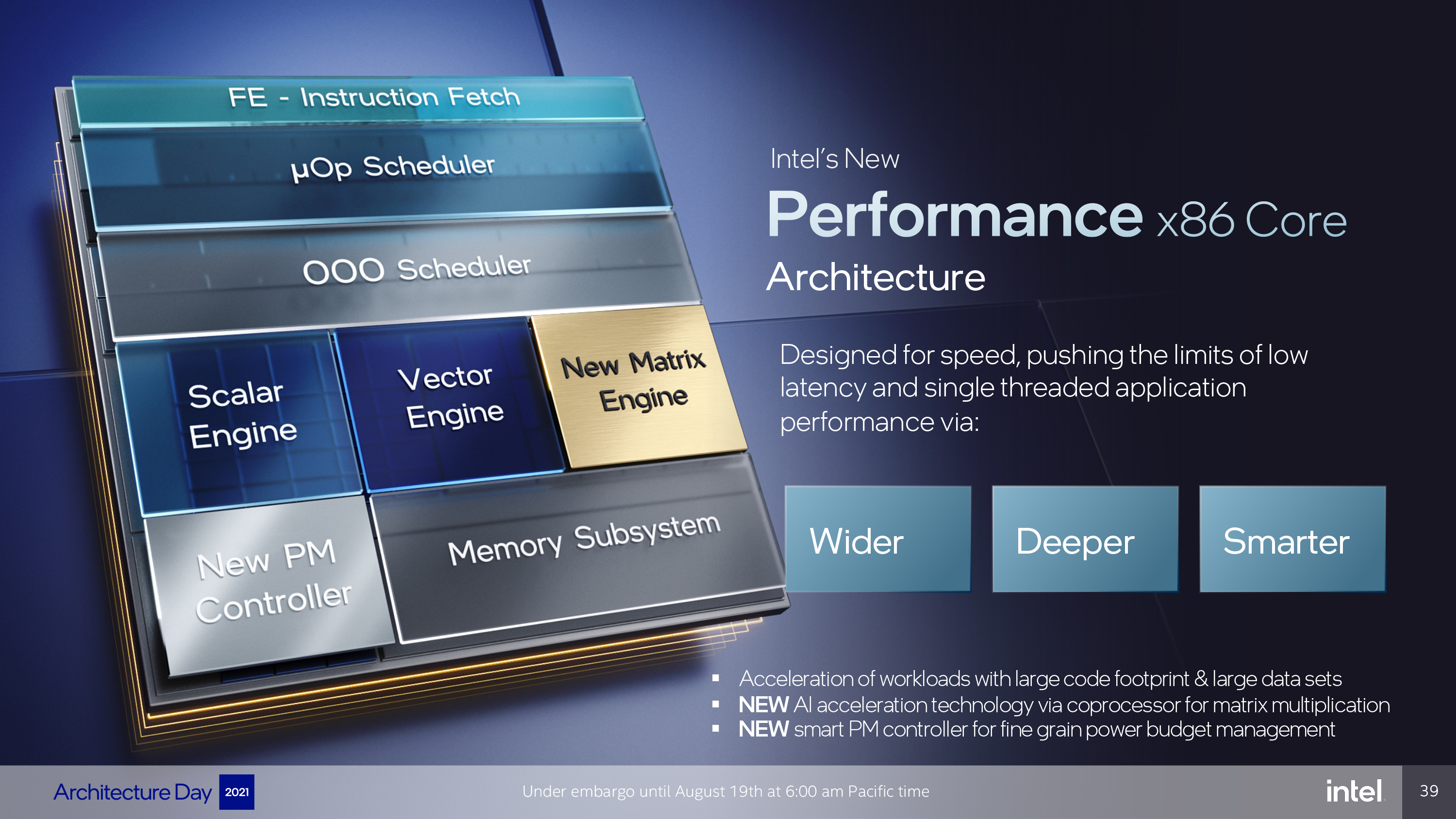
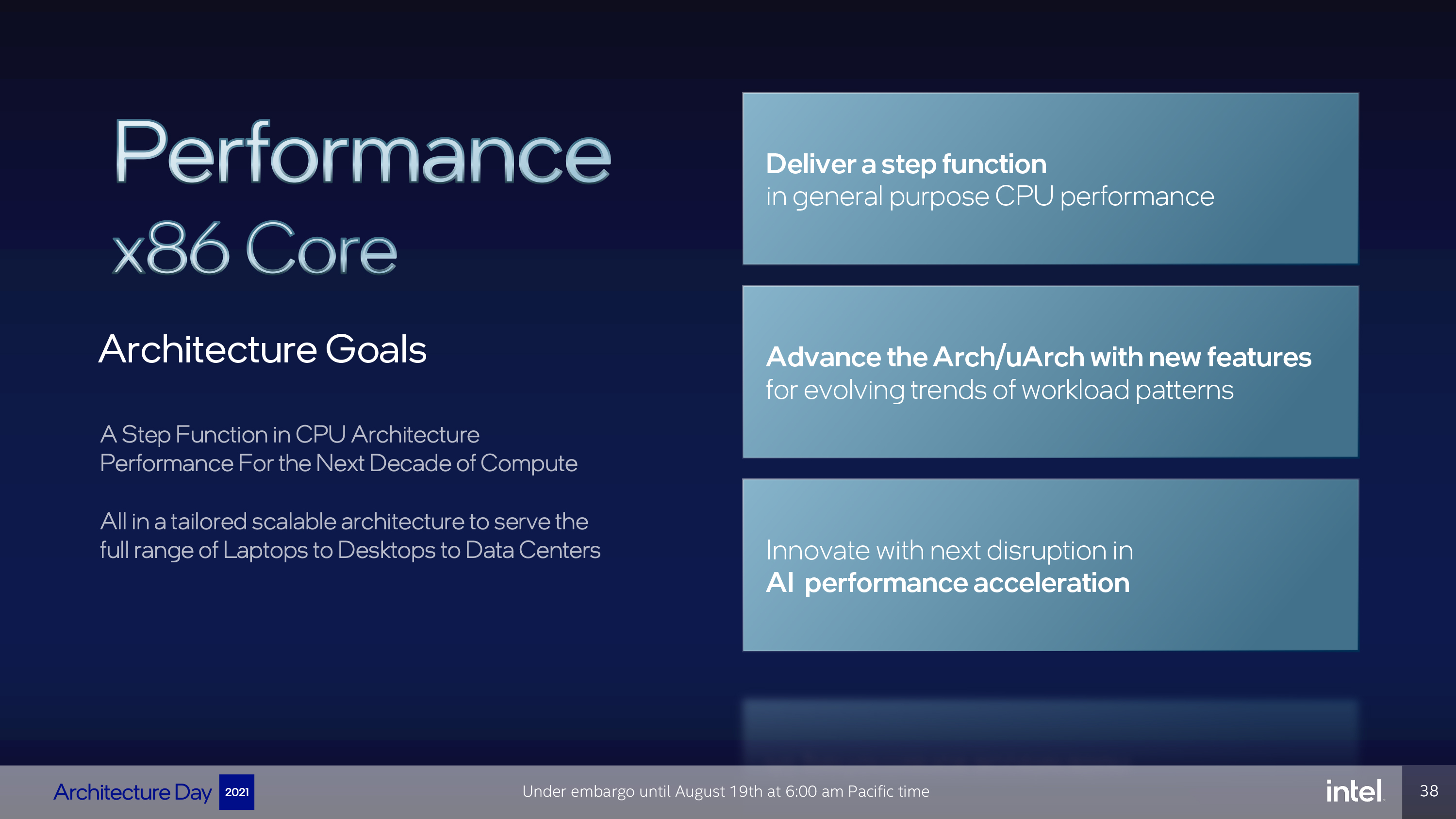
Intel's goal with its Performance Core (P-Core), which comes with the Golden Cove microarchitecture, was to create the highest-performance core the company has ever built and deliver a step-function increase in CPU performance. However, the architecture also needed to be scalable with a wide dynamic range so it could scale from laptops to desktops to data centers — Intel uses this same core in its Sapphire Rapids server chips, too, albeit with modifications that tailor it for datacenter workloads.
For the client market, the company focused on optimizing the core for single-threaded performance and AI workloads. The company also wanted to expand its support for large data sets and large code footprint applications.
As we've seen in the past, Intel followed the "Wider, Deeper, Smarter" ethos with the Golden Cove design. That includes a deeper out of order scheduler and buffers, more physical registers, a wider allocation window, and more execution ports. Intel paired those enhancements, which we'll cover below, with smarter branch prediction to better feed the execution engine, thus unlocking more parallelism and performance.
The company also ingrained a new autonomous power management microcontroller into each core that measures telemetry at microsecond granularity, instead of milliseconds. Intel says this allows them to better optimize power usage based on the actual behavior of an application, thus delivering higher average frequency for any workload. This is Intel's first per-core integrated power management microcontroller, and it is only present on the Golden Cove cores.
We surmise that this unit also feeds Intel's Thread Director tech with telemetry data. The power management controller also allows for faster frequency transitions, though Intel hasn't said just how fast. Alder Lake still adjusts frequency in 100 MHz steps, though, as opposed to Zen's 25 MHz granularity.
Here's the short list of improvements that we'll cover below.
| Unit | Sunny Cove | Performance-core |
|---|---|---|
| iTLB 4K pages | 128 | 256 |
| iTLB 2M/4M | 16 | 32 |
| uop Cache | 2.25K | 4K |
| uop cache BW | 6 | 8 |
| Decoders | 4 | 6 |
| Allocation | 5 | 6 |
| OoO Window | 352 | 512 |
| Integer ALUs | 4 | 5 |
| # of Loads | 2×512 | 3×256, 2×512 |
| L1 data Cache | 48KB | 48KB |
| L1 Fill Buffers | 12 | 16 |
| L1 DTLB | 64 | 96 |
| L2 cache | 512KB/1.25MB | 1.25MB / 2MB |
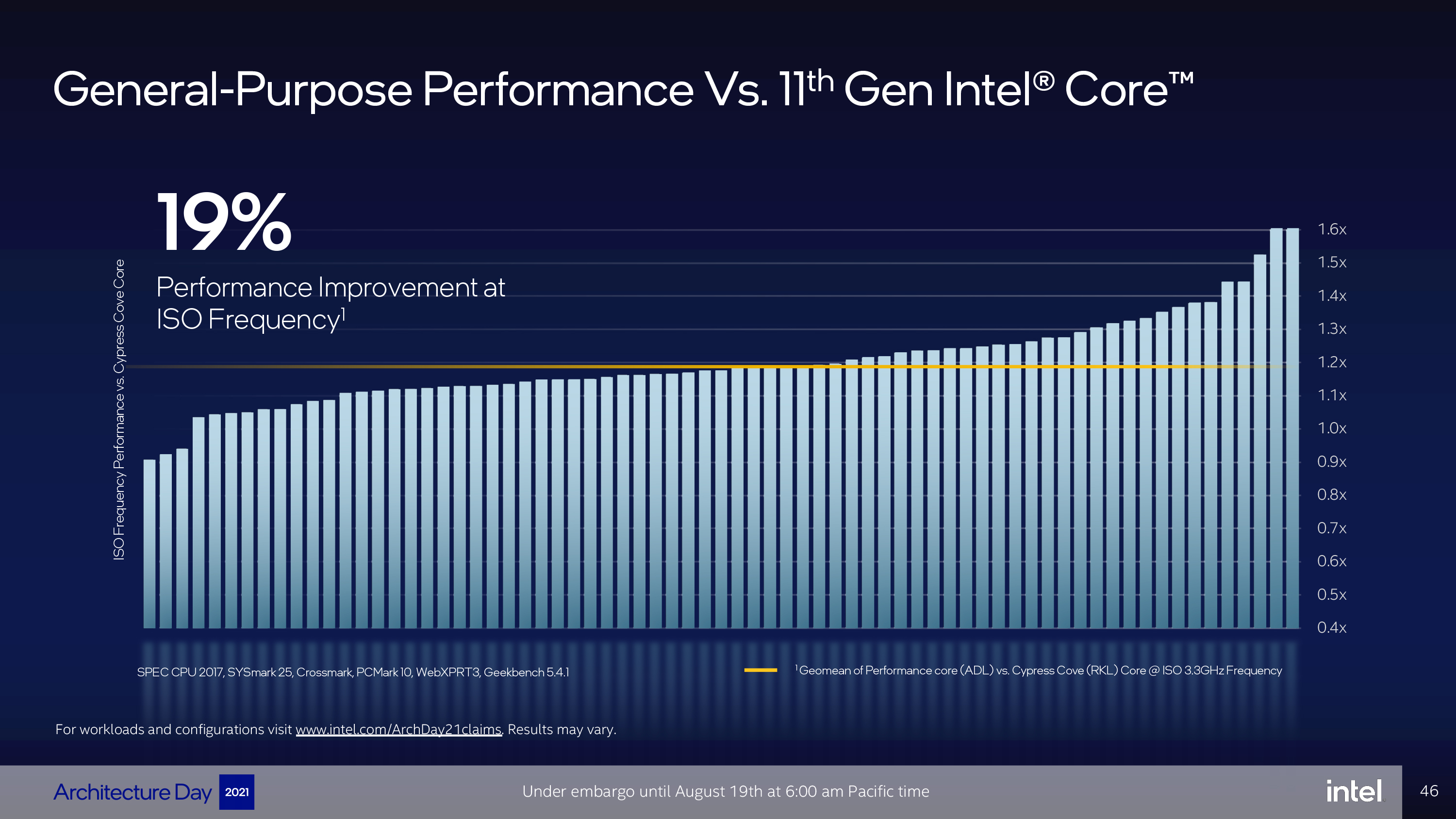
We'll jump ahead here and show you Intel's claimed results, and then show you how Intel got there. Intel claims that Alder Lake's Golden Cove performance core offers an average of a 19% performance improvement over the Cypress Cove architecture found in Rocket Lake when both chips operate at the same frequency (ISO frequency). Intel derived this average from a wide distribution of workloads that includes SPEC CPU 2017, Sysmark 25, Crossmark, PCMark 10, WebXPRT3, and Geekbench, among other unlisted benchmarks.
Get Tom's Hardware's best news and in-depth reviews, straight to your inbox.
As with all vendor-provided benchmarks, you'll have to take this with a grain of salt. But this could be promising if Intel can deliver near these levels of performance improvements, assuming it can squeeze high enough clock rates out of the Intel 7 silicon and workloads can be correctly targeted to these performance cores, of course.
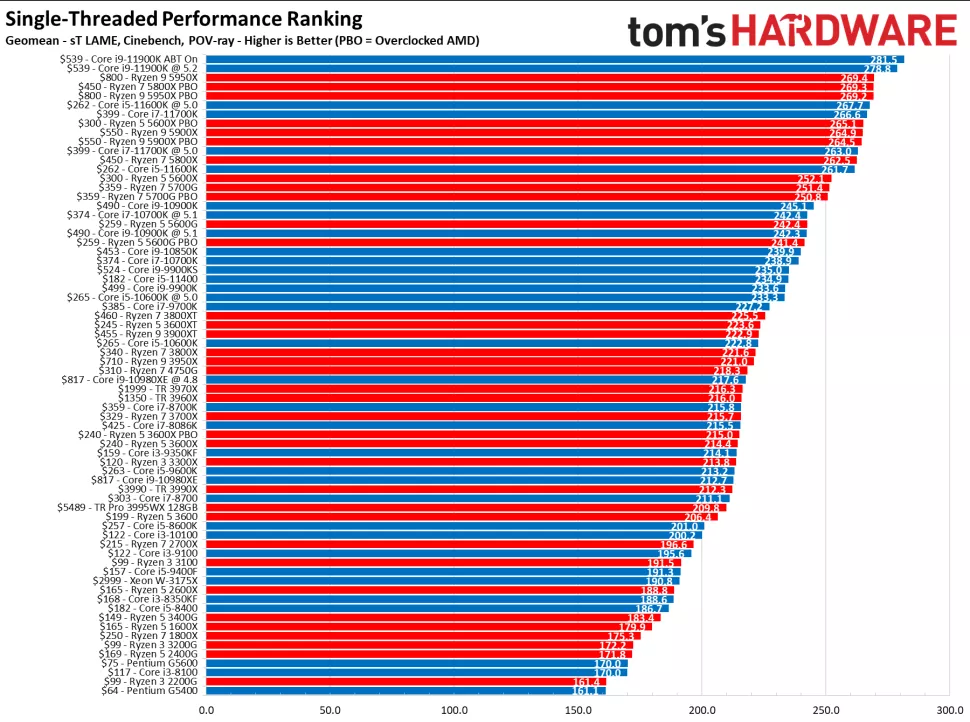
Intel claims this jump is larger than the improvement from Skylake to Sunny Cove. That's impressive, if true. The second image in the album above comes from our lab results in our CPU Benchmark hierarchy. Intel's Rocket Lake Core i9-11900K, which has the Cypress Cove architecture that is very similar to Sunny Cove, currently leads the single-threaded performance hierarchy against AMD's chips. A quick glance at Intel's previous-gen Core i9-10900K shows that Intel's jump from Skylake to Sunny Cove represented a large improvement that helped it take the lead from AMD's Zen 3 architecture. That means Alder Lake's single-threaded performance could be well-positioned against AMD's Zen 4 chips if it can pull off a comparable advance.
Front End
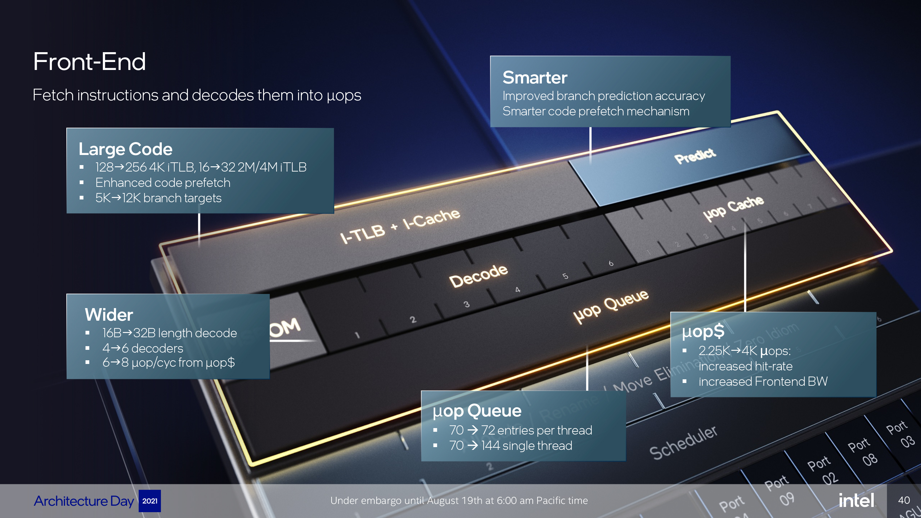
Intel improved the micro-op supply from both the decoder and the micro-op cache. That starts by doubling length decode to 32B per cycle and adding two additional decoders (6) to enable 6 decodes per cycle. The micro-op cache also now feeds 8 micro-ops per cycle instead of 6 and can hold 4K micro-ops, up from 2.25K before. This helps to feed the out of order engine quicker and increases the micro-op hit rate.
To support software with a large code footprint, Intel doubled the number of 4K pages and large pages stored in the iTLB (as listed in the table above) and enhanced code prefetch by increasing from tracking 5K branch targets to 12K branch targets.
Intel says it improved branch prediction to reduce jump mispredicts and significantly overhauled the Branch Target Buffer (BTB). The BTB serves as a cache for the prefetcher, and Intel more than doubled it to help with large code footprints. Additionally, the BTB now has a machine learning algorithm that allows it to expand or contract capacity based upon usage, thus fine-tuning power and performance.
Out of Order Engine
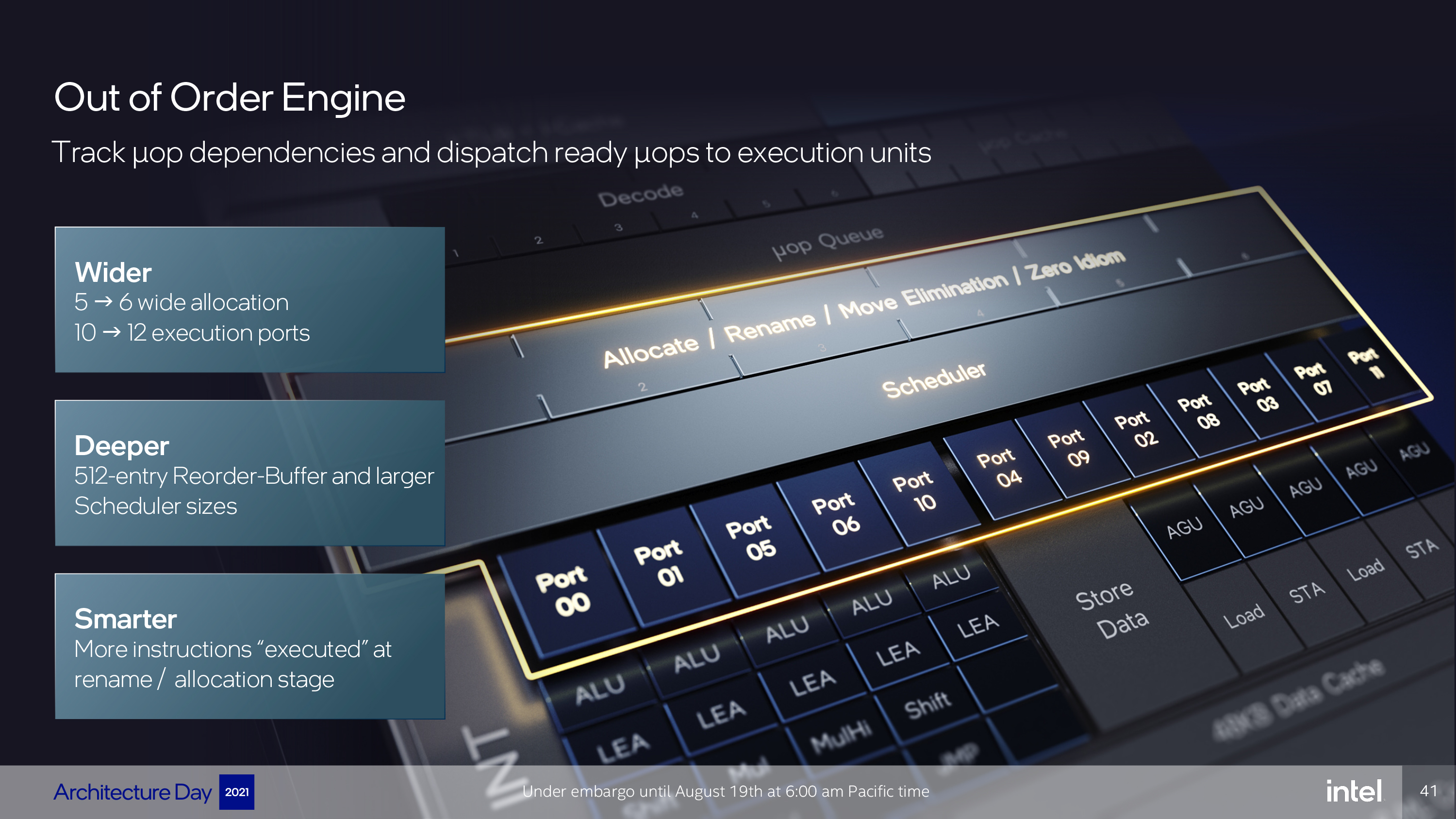
Intel widened the Out of Order (OoO) engine from a 5- to 6-wide allocate unit that then feeds into the scheduler, which now feeds 12 execution ports, as opposed to 10 with Sunny Cove. The engine is also deeper with a 512-entry reorder-buffer, up from 352, and more physical registers.
Intel also says that it has enabled collapsing dependency chains by executing some simple instructions at the rename/allocation stage to save resources further down the pipeline. This allows other operations to run faster and save power by better utilizing the instruction resources. Intel is playing coy about this new technique, though, and hasn't answered follow up questions regarding its new technique.
Integer and Vector Execution Units
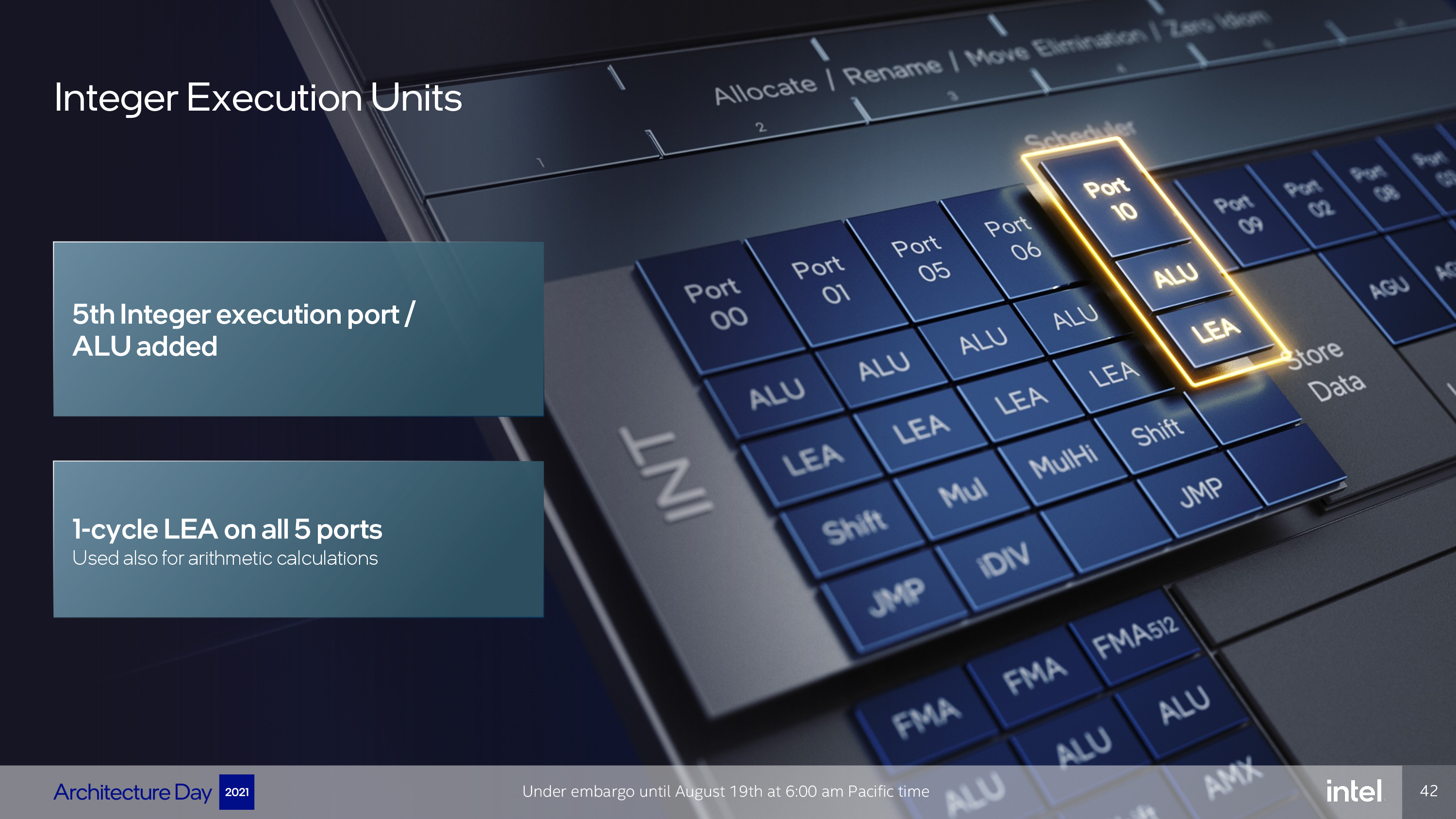
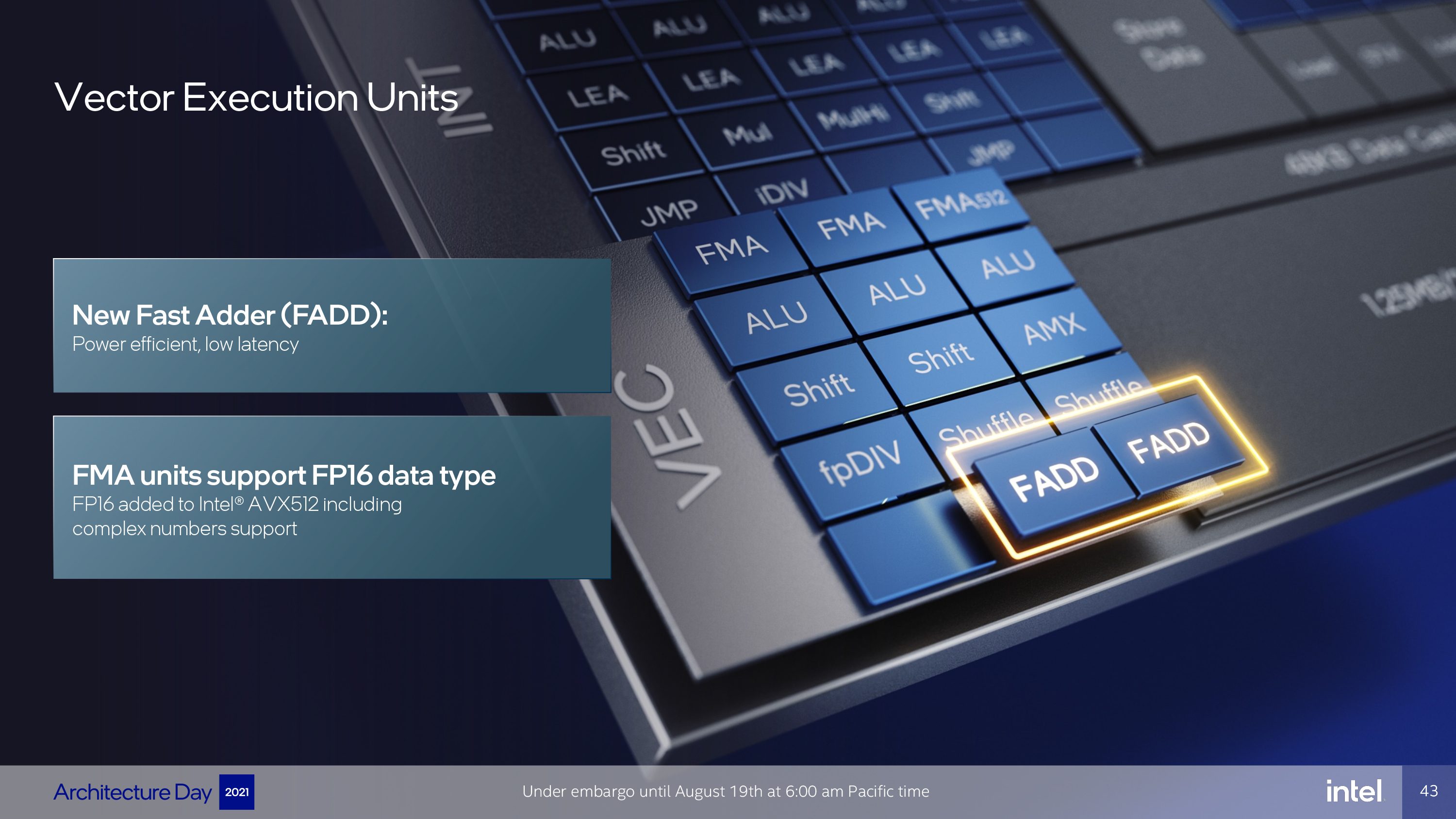
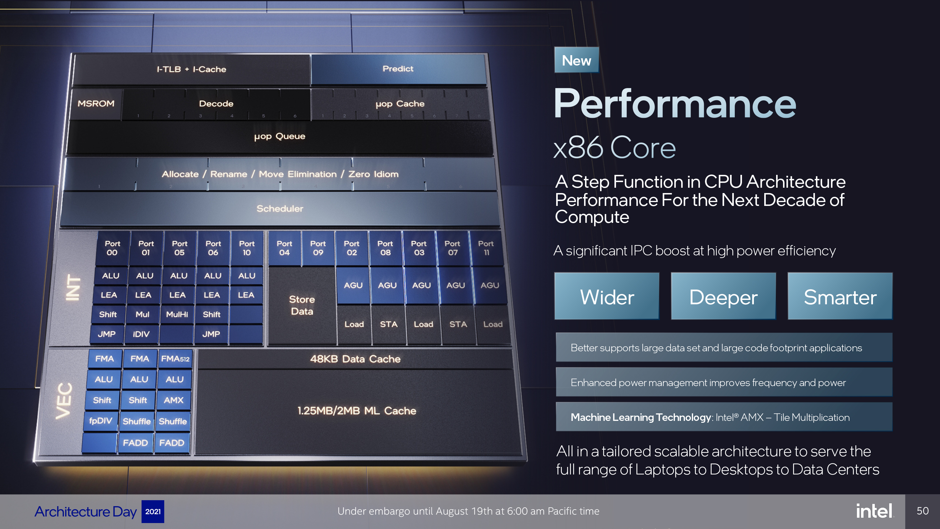
Intel added a fifth general integer execution port with an ALU and LEA. All five LEAs are single-cycle and can be used for additions and subtractions, or fast multiplications with fixed numbers. On the vector side, Intel infused two more fast adders (FADD) on ports 1 and 5. Intel also bulked up the FMAs with support for FP16 operations with AVX-512 instructions, but that is confined to the server versions of the chip. AVX-512 is disabled for Alder Lake processors.
L1 and L2 Cache and Memory Subsystems
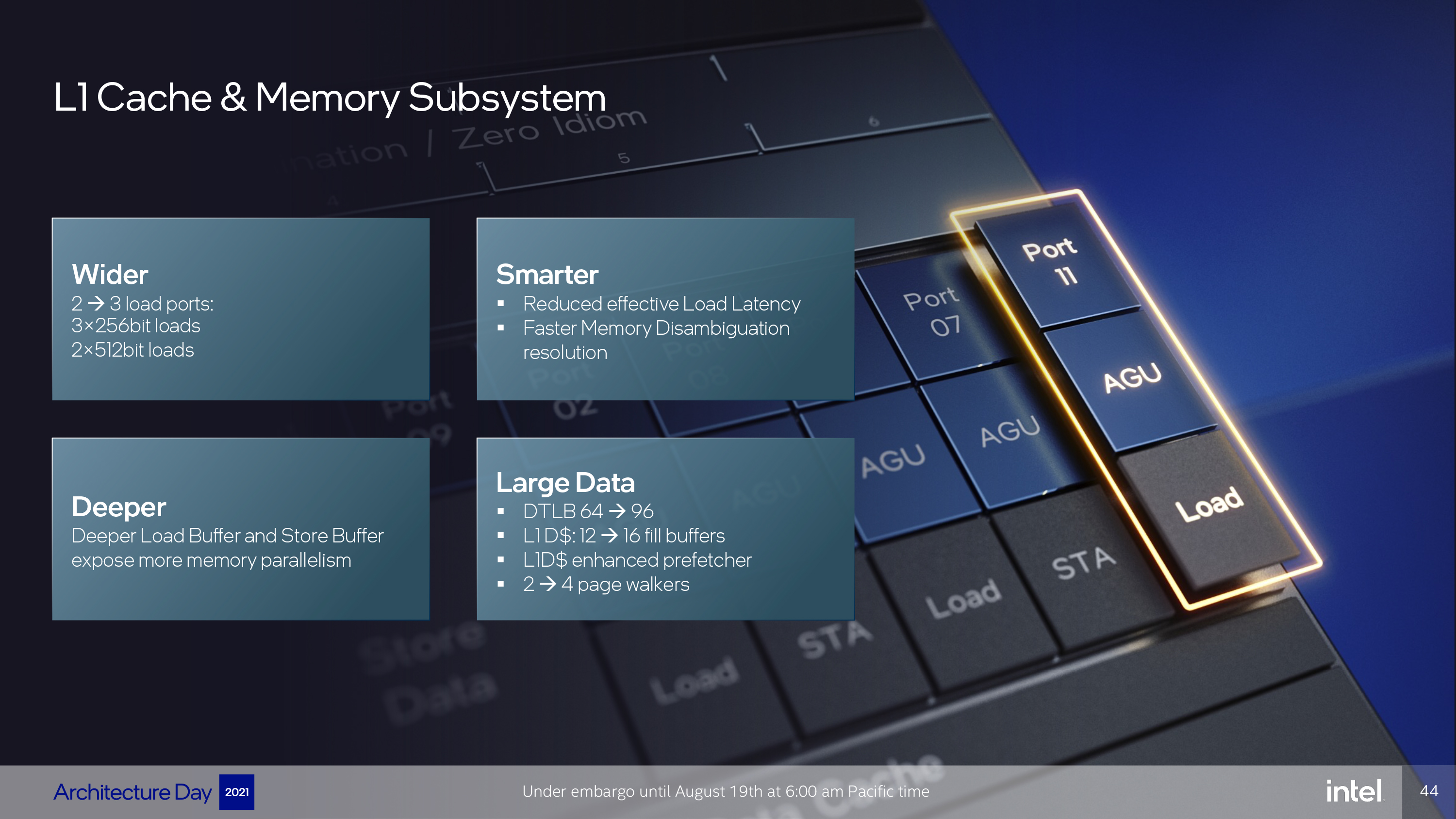
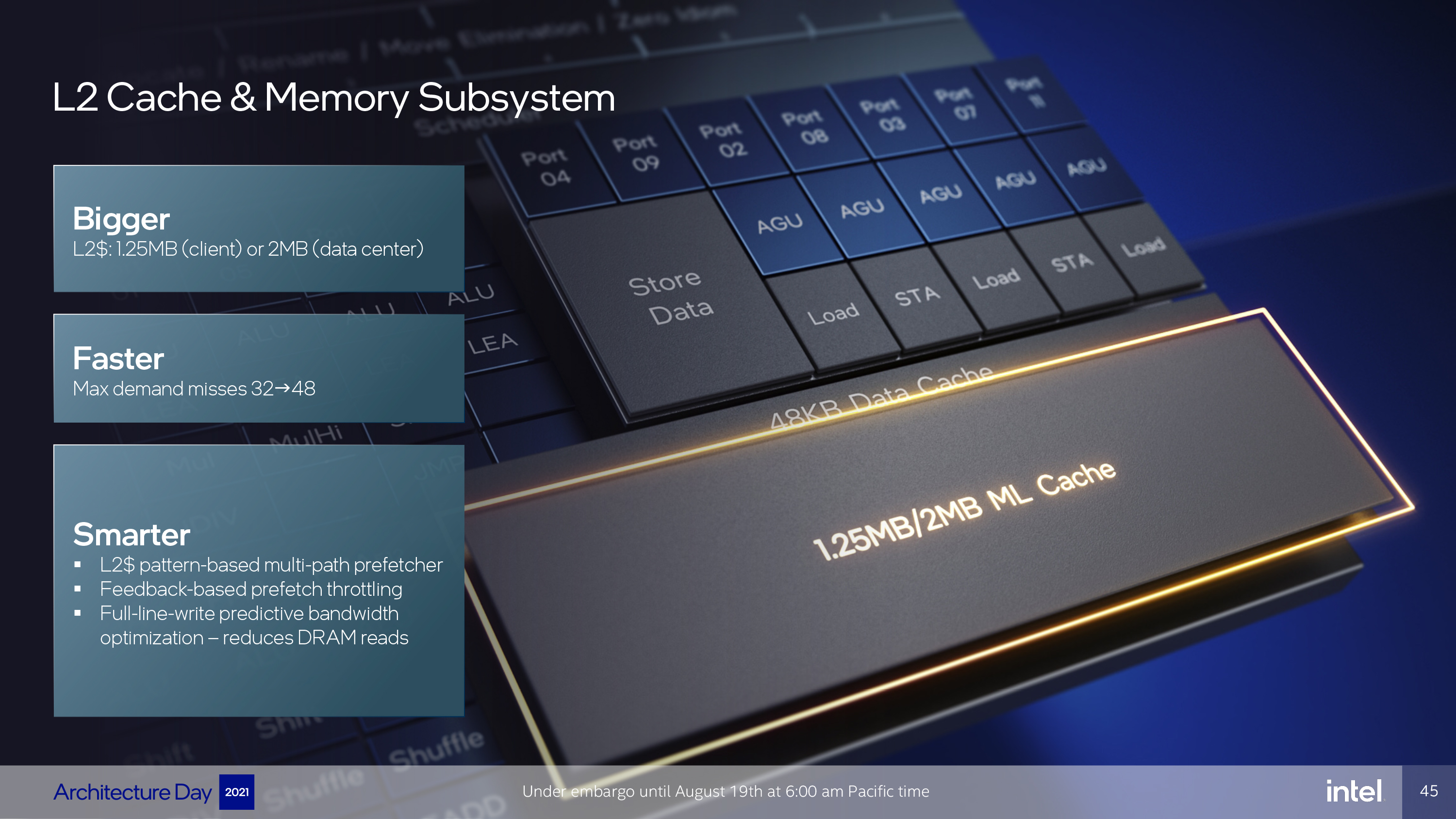
The L1 cache is now wider with 3 load ports instead of 2, and deeper with larger Load and Store Buffers. Intel increased the L1 data TLB by 50% and the L1 data cache can fetch 25% more misses in parallel. The L1-D cache also has an enhanced prefetcher that can now service four page table walks instead of two, which is good for workloads with irregular data sets.
The consumer chips, like Alder Lake, will come with 1.25MB of cache per performance core, while data center chips get 2MB. The lower-capacity cache for client results in improved latency, while the higher-capacity cache for datacenter helps feed chips with higher core counts. Intel says its new prefetch engine observes running programs to identify potential future memory access patterns, and then can prefetch down multiple potential paths to service those potential requests.

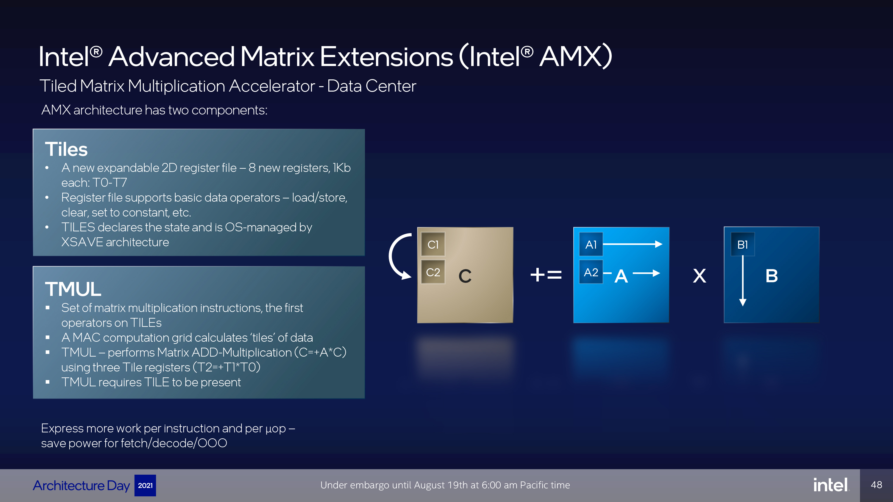
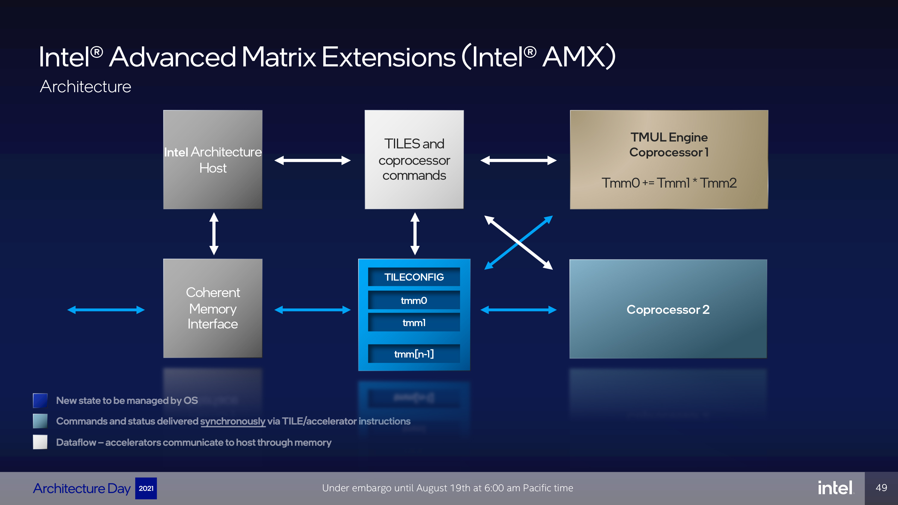
Intel's Advanced Matrix Extension (AMX) technology is disabled in the Golden Cove cores present in Alder Lake but is active for the Sapphire Rapids datacenter processors. AMX is a next-gen AI accelerator that enables hardware-accelerated matrix multiplication operations that significantly enhance AI inference and training performance. Like AVX, AMX incurs a clock frequency penalty. To reduce jitter, Intel has worked to reduce the impact of the AMX license levels on clock rates, largely by adopting a more fine-grained per-core power control scheme. We'll dive deeper into this technology in our Sapphire Rapids coverage.
Current page: Intel Alder Lake Golden Cove Performance Core
Prev Page Intel Alder Lake Gracemont Efficiency Core Next Page Thoughts
Paul Alcorn is the Editor-in-Chief for Tom's Hardware US. He also writes news and reviews on CPUs, storage, and enterprise hardware.
-
TerryLaze ReplyAlder Lake does not support AVX-512 under any condition (fused off in P cores, not supported in E cores).
Called it that all they need to do to get power draw down to ryzen levels is to turn off avx.
If they also locked down power limits, at least on non OC boards, they can sell it as super future low power tech. -
JWNoctis No AVX-512 at all?...Yeah, that's gonna be a rather huge regression for those applications that made use of them, which is admittedly uncommon in consumer space.Reply
But then there's not that much difference between Core, Pentium, and Celeron lines anymore, unless they are going to detune IPC in microcode or something. What's the name of the next one, I wonder? -
TerryLaze Reply
Rocketlake didn't get any pentiums or celerons, no reason to believe that alder lake will have them.JWNoctis said:No AVX-512 at all?...Yeah, that's gonna be a rather huge regression for those applications that made use of them, which is admittedly uncommon in consumer space.
But then there's not that much difference between Core, Pentium, and Celeron lines anymore, unless they are going to detune IPC in microcode or something. What's the name of the next one, I wonder?
Now the celeron (atom) is going to be integrated in the core... :p -
Giroro Intel keeps talking up how great their tiny gracemont cores are... But if 4 gracemont cores were able to outperform 1 Golden Cove core, then the entire CPU would be gracemont. I think its no coincidence that their desktop CPUs tacked on exactly enough tiny cores to confuse people into thinking they have parity with 16-core ryzen. Just like how they renamed their 10nm process to give the illusion of parity.Reply
I have no confidence whatsoever that their 8C/8c/24t processor has better multithreaded performance than a hypothetical 10C/0c/20t processor. If that were the case, then the configurations would be more like 0C/40c/40t... Or maybe even 2C/32c/36t.
But no, this is all about how they can technically get away with selling what is essentially an 8 core processor, using a giant sign that says 16 CORES* WORLD'S BEST EFFICIENCY**!
They at least know performance matters a little bit, because a 40 CORE CPU has to got be pretty tempting to somebody in their marketing department, regardless of how bad it would be. -
Johnpombrio This will probably be my next CPU replacing my i9-9900K. I need at least PCI-4.0 for my 2TB Samsung 980 Pro ($313 lightning deal in Amazon Prime day in June). I will never need all of these cores tho.Reply -
mdd1963 Cautiously optimistic, but, I recall feeling the same way before 11th gen released...Reply
This time I will be pessimistic until happily (hopefully) proven wrong. :)
(Need some BF1/BF5 1080P benchmarks to truly know if Alder Lake is 'mo betta'!) -
JamesJones44 ReplyGiroro said:Intel keeps talking up how great their tiny gracemont cores are... But if 4 gracemont cores were able to outperform 1 Golden Cove core, then the entire CPU would be gracemont. I think its no coincidence that their desktop CPUs tacked on exactly enough tiny cores to confuse people into thinking they have parity with 16-core ryzen. Just like how they renamed their 10nm process to give the illusion of parity.
I have no confidence whatsoever that their 8C/8c/24t processor has better multithreaded performance than a hypothetical 10C/0c/20t processor. If that were the case, then the configurations would be more like 0C/40c/40t... Or maybe even 2C/32c/36t.
But no, this is all about how they can technically get away with selling what is essentially an 8 core processor, using a giant sign that says 16 CORES* WORLD'S BEST EFFICIENCY**!
They at least know performance matters a little bit, because a 40 CORE CPU has to got be pretty tempting to somebody in their marketing department, regardless of how bad it would be.
How do you explain M1s multi thread performance then, the quote makes little sense. There is a lot more to CPU design than the number of cores and their single thread IPC. I don't claim to know if they will be able to compete with a 10 big core CPU, but the M1 and other hybrid architectures prove that very good multi thread performance can be had with the big little design. -
ezst036 ReplyGiroro said:I think its no coincidence that their desktop CPUs tacked on exactly enough tiny cores to confuse people into thinking they have parity with 16-core ryzen. Just like how they renamed their 10nm process to give the illusion of parity.
There may be some of that, but Intel at this point can afford to cede some of the high end to AMD. They don't have to outright win, they just have to be competitive enough. And Intel is also prepping to fight AMD as well on the GPU front.(also nVidia)
Intel's biggest threat is ARM. They cannot afford to keep taking it on the chin any longer in mobile. Alder Lake big.little will be a game changer even if it doesn't get the final mile to energy efficiency utopia.
But really, I think people also forget or they discount that the pressure from manufacturing also is playing a factor here. Intel's fab woes go back how many years now? Intel needs small cores partially, and manufacturing woes in all sectors of chip manufacturing is going to force AMD to do the same with big.LITTLE. They've got Jaguar or Bobcat or whatever the latest iteration of that little core was, it won't be long before it's tacked on for some AMD big.LITTLE also.
16 big cores is simply more stress on manufacturing than 8 big and 8 small when you factor in the big picture and tons of silicon wafer after wafer after wafer. Alder Lake helps Intel to help Intel out on their fab woes. -
ezst036 ReplyJamesJones44 said:How do you explain M1s multi thread performance then
You only need one word.
Optimization.
Apple controls all aspects of MacOS, and are particularly fans of cutting off their own customers after so many years. They don't want, don't need, and simply don't carry a lot of legacy "baggage" - even if you spent $8000 on your computer. Apple will cut you off.
You explain M1 performance with optimizations under the hood.
