Intel's Ivy Bridge CPU Die Layout Estimated
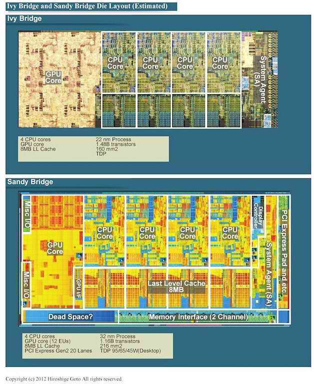
With Ivy Bridge a little over a month away, Hiroshige Goto, contributor for PC Watch, has estimated the layout of Ivy Bridge silicon.
Get Tom's Hardware's best news and in-depth reviews, straight to your inbox.
You are now subscribed
Your newsletter sign-up was successful
As discussed at the IEEE International Solid-State Circuits Conference, Intel engineer Scott Siers announced that there will be four different Ivy Bridge die models. In addition, Ivy Bridge will carry up to 1.4 billion transistors that span over an area of 160 mm2, which is about 26 percent smaller than the comparable 216 mm2 Sandy Bridge die with 1.16 billion transistors. Ivy Bridge is built on 22 nm process, which is the "tick" process of Intel's Tick Tock Model.
Taking a closer look at the Ivy Bridge's estimated die layout, the layout is similar in design to current-gen Sandy Bridge. The die is made up of three general sections, 1) CPU cores, 2) System Agent and 3) Graphics core.
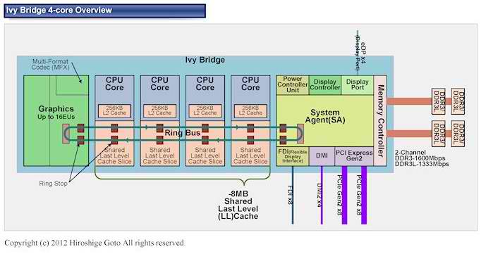
The CPU cores are made up of four x86-64 cores with 256 KB dedicated L2 cache per core and shared 8 MB L3 cache. The System Agent holds the dual-channel DDR3 integrated memory controller (DDR3 1600), a PCIe interface (as a shared x16 port or two separate x8 ports), a DMI link, a display controller, power controller unit, and a FDI link. The Graphics Core has 16 programmable EUs that handle parallel processing loads for the GPU and can be programmed to perform GPGPU tasks. In addition, it holds the Multi-Format CODEC, which supports MPEG2, VC1, AVC and also MVC (multi-view video coding) for stereoscopic 3D. All the components are bound by a ring-bus that transports tagged data between the CPU cores, the graphics core, the L3 cache, and the system agent.
Article continues belowAs Scott Siers announced, there will be four different variants of the Ivy Bridge die models.
- 4+2: All four cores enabled, full 8 MB L3 cache enabled, all 16 shader cores (EUs) of the IGP enabled
- 2+2: Two cores enabled, 4 MB L3 cache enabled, all 16 shader cores of the IGP enabled
- 4+1: All four cores enabled, 6 MB L3 cache enabled, fewer shader cores of the IGP enabled
- 2+1: Two cores enabled, 3 MB L3 cache enabled, fewer shader cores of the IGP enabled
Get Tom's Hardware's best news and in-depth reviews, straight to your inbox.
-
ojas I wonder if they'd keep the die size the same as sandy bridge, wouldn't that let them stuff more things like cache and IGP shaders (or whatever IGPs have) in the same space?Reply -
memadmax The tick tock model is why intel will always be the innovator, and AMD the follower...Reply -
hardcore_gamer 1/3 rd of the die area is taken by the crappy GPU cores. They should have used it for additional logic or cache to speed up the CPU, atleast for the K series CPUs since the people who buy them use a discrete GPU anyway.Reply -
@hardcore_gamerReply
Ivy bridge and the rest of LGA1155 is ment for the low-mid range market segments, where people want the build-in graphics. Sure most people who buy the K CPUs probably wont ever use the GPU, but it would probably be too expensive to change the layout just for the K modules, not to mention that it would be a completely different design, which kinda goes against the tick-tock model.
If you wanted to use discrete GPUs, you should go with the SNB-E, Ivybridge-E LGA2011 series, atleast following Intels logic :) -
killabanks memadmaxThe tick tock model is why intel will always be the innovator, and AMD the follower...more like billions of $$ means intel will always be ahead of amdReply -
fuzznarf hardcore_gamer1/3 rd of the die area is taken by the crappy GPU cores. They should have used it for additional logic or cache to speed up the CPU, atleast for the K series CPUs since the people who buy them use a discrete GPU anyway. Yeah, you're right. Intel probably has no idea what they are doing....Reply -
gilbertfh I am excited... I skipped Sandy since I considered her a 7. Hopefully Ivy will be a 10 and age well.Reply -
bartholomew killabanksmore like billions of $$ means intel will always be ahead of amd:D & Only the ones with lots of $$ can afford their best CPUs :PReply -
builder4 hardcore_gamer1/3 rd of the die area is taken by the crappy GPU cores. They should have used it for additional logic or cache to speed up the CPU, atleast for the K series CPUs since the people who buy them use a discrete GPU anyway.Reply
They don't want to completely smash AMD by speeding up the CPU. Intel relies on AMD's continual existance to prevent the government splitting them up on monopoly grounds. As long as AMD is non competitive, intel won't increase the CPU performance of their mainstream chips.
They do, however, offer a larger die and more CPU cores replacing the GPU on the 2011 platform for 3x the price. -
mindless728 Reply9348674 said:1/3 rd of the die area is taken by the crappy GPU cores. They should have used it for additional logic or cache to speed up the CPU, atleast for the K series CPUs since the people who buy them use a discrete GPU anyway.
not everynody buys the K series for gaming, I bought one for a minecraft server just to OC it to a pale 4GHz (don't need extreme), as it is a lot cheaper then buying server grade and also let me OC if need be

