AMD Demos The World's First 7nm GPU, Radeon Instinct Vega
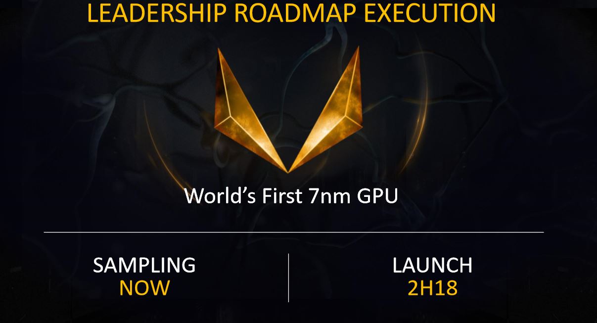
AMD's Lisa Su displayed the world's first 7nm GPU die at Computex 2018. The package is complemented by 32GB of HBM2 memory and drops into the company's new Radeon Instinct Vega GPUs. Unfortunately for the enthusiasts among us, AMD designed the Instinct cards to capture the exploding data center AI and machine learning market, but Su assured the crowd that the company plans to bring the new process to consumer GPUs in the future. Su didn't specify if the new gaming graphics card would feature the Vega architecture, but we expect it to come with the next-gen Navi architecture.
AMD's David Wang also announced that the company is striving to produce a new graphics product every year for the next three years, which bodes well for a consumer graphics market that has become somewhat stagnant in terms of recently released high-end graphics cards.
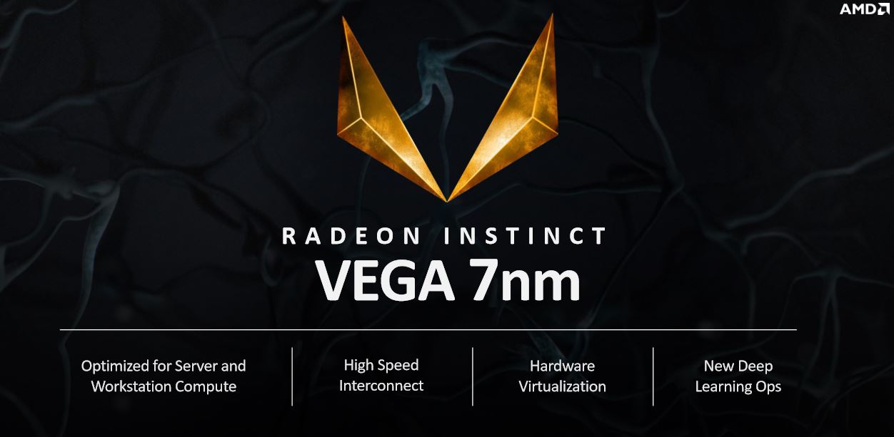
AMD is currently sampling the 7nm Vega GPU to its partners and will launch it to the general market in the second half of 2018. That's a full quarter ahead of expectations. The card comes bearing the fifth-gen GCN microarchitecture, but it will bring many of the benefits borne of the 7nm process. In addition, true to the GPUs' stated mission, the card has a number of optimizations specifically for AI workloads.
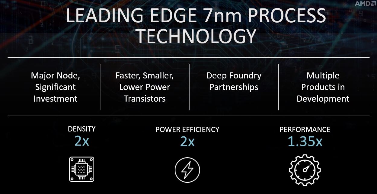
Article continues belowAMD claims the new 7nm process is twice as dense as its 14nm process, and the 7nm Vega die appears to be roughly 40% smaller than its predecessor. The new process also affords a 2x increase in power efficiency and AMD also claims it provides a 1.35x increase in performance. This very specific metric indicates that AMD is relatively far down the development path with its working silicon. The company seems increasingly confident with the new 7nm process, as evidenced by its demo of a 7nm EPYC CPU at the same event.
Another fundamental change comes in the form of the Infinity Fabric. AMD designed this coherent interconnect to facilitate communication between its components inside discrete packages, as we see with the Ryzen and Threadripper processors. It also makes an appearance in the Vega 10 for intra-device communication.
AMD's new tactic extends the fabric outside of the GPU to speed peer-to-peer (P2P) communication between GPUs. This approach is similar to Nvidia's NVLink implementation, so it purportedly reduces latency and boosts throughput between graphics cards. We've seen several other P2P implementations take root in the broader component landscape, such as P2P fabrics that speed communication between storage devices and GPUs, but it appears the industry is stratifying into proprietary solutions.
In either case, it's logical to expect the Infinity Fabric to eventually extend to communication between the CPU and GPU, which could provide AMD yet another advantage as the only producer of both x86 processors and GPUs. Interconnects are increasingly becoming more of a strategic asset as companies transition to heterogeneous computing architectures, and it's a positive sign that AMD's Infinity Fabric continues to pay dividends.
Get Tom's Hardware's best news and in-depth reviews, straight to your inbox.
AMD has also infused the GPU with support for a new set of deep learning operations that are likely designed to boost performance and efficiency.
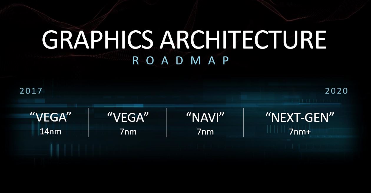

AMD originally planned to release 12nm GPUs, which it announced last year, but made the strategic decision to remove those products from the roadmap and skip to the 7nm process instead. AMD has 7nm Navi up next on its roadmap, followed by new graphics cards with a 7nm+ process that should arrive before the end of 2020.
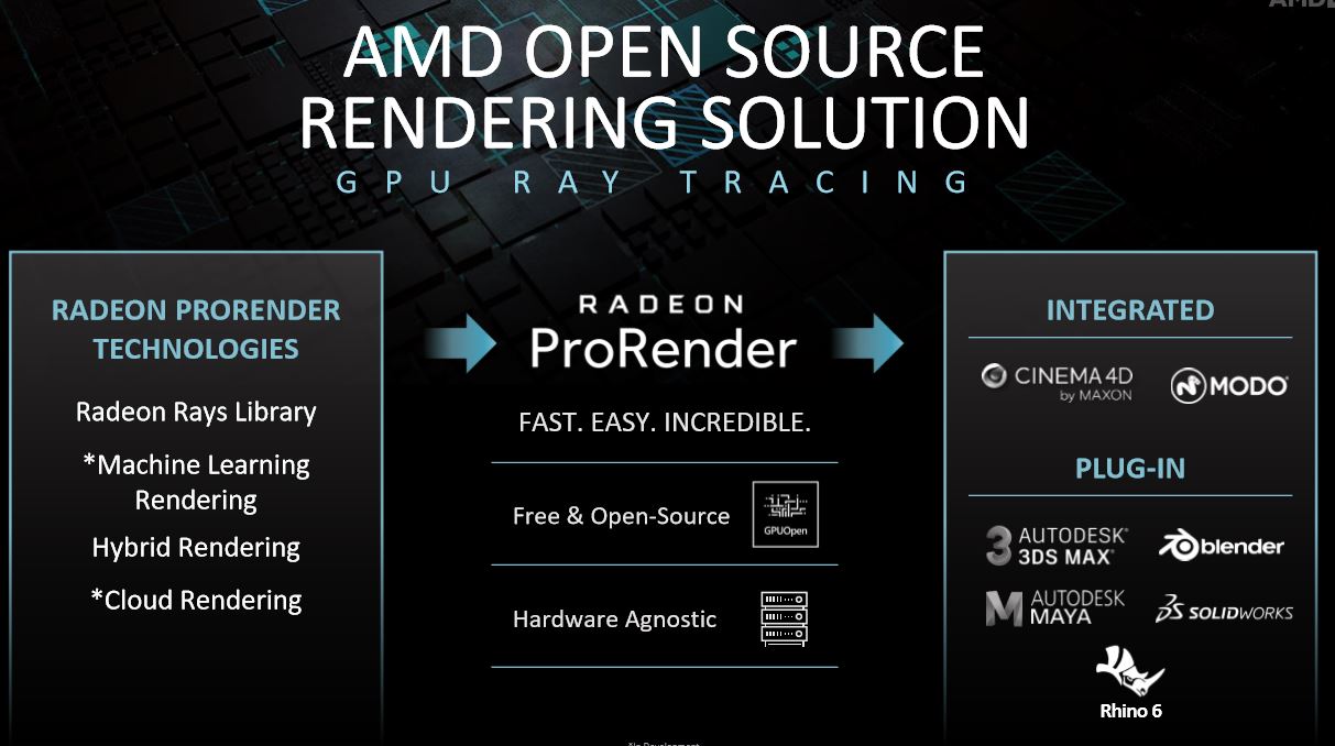
AMD demoed the GPU running a Cinema4D rendering workload with the company's open-source Radeon Pro Render ray tracing solution. AMD continues to leverage the open source community for its Radeon Open Ecosystem (ROCm) software solutions, which stands in stark contrast to other vendors' proprietary software, like CUDA.
Neural networks are becoming increasingly complex, and, as a byproduct, voluminous, so AI-driven architectures increasingly require more memory capacity to keep pace. AMD's 32GB of HBM2 should put the company on par with Nvidia's recent adjustment that boosts the Tesla V100 up to 32GB, but we aren't sure if AMD will also offer versions with 16GB of HBM2. That could be an asset given the current sky-high pricing for HBM2 memory. AMD didn't reveal specifications or pricing for the new cards or a definitive timeline for mainstream graphics cards.

Paul Alcorn is the Editor-in-Chief for Tom's Hardware US. He also writes news and reviews on CPUs, storage, and enterprise hardware.
-
oneblackened This is a big deal. AMD has beaten both Nvidia and Intel to the punch on process node shrinks.Reply -
bit_user Reply
Moot point, given that it hasn't got tensor cores. Okay, I'm assuming it doesn't have tensor cores, but I'm pretty sure she'd have mentioned them if it did. So, even with the 35% performance boost, it still can't touch the training performance or efficiency of Nvidia's V100.21035041 said:This is a big deal. AMD has beaten both Nvidia and Intel to the punch on process node shrinks.
BTW, the new instructions will help for inference, but not training.
-
Gary_133 AMD skipping 12nm and going straight to 7nm? That brings a tear to the eye in a very good way!!Reply
Nothing but praise the way Lisa Su is running the company placing technical improvements just as high as profits! -
InvalidError Reply
A tensor core is only a fancy name for matrix multiply-add. AMD could probably tweak the shader architecture to achieve comparable performance without dedicating a large chunk of die area to fixed-function math, albeit at the expense of power efficiency when running tensor-intensive workloads.21035085 said:Moot point, given that it hasn't got tensor cores. Okay, I'm assuming it doesn't have tensor cores, but I'm pretty sure she'd have mentioned them if it did. -
boju AMD have sailed their Chips over the narrow sea. The big war is coming who will prevail. Will it be the Advanced Mother of Dragons, the Nviannister's or the Intelwalker's. Winter is coming The night is dark and full of terrors, old man, but the fire burns them all away." "Look to your sins Lord Renly, the night is dark and full of terrors.Reply
-
bit_user Reply
Vega already had packed fp16 math, and (as I implied) I've already seen enough of the LLVM patches for the new instructions to know that they won't significantly change its fp16 throughput.21035180 said:
A tensor core is only a fancy name for matrix multiply-add. AMD could probably tweak the shader architecture to achieve comparable performance without dedicating a large chunk of die area to fixed-function math, albeit at the expense of power efficiency when running tensor-intensive workloads.21035085 said:Moot point, given that it hasn't got tensor cores. Okay, I'm assuming it doesn't have tensor cores, but I'm pretty sure she'd have mentioned them if it did.
So, the only way it gets more than the stated 35% performance boost @ training is by some fixed-function hardware that wasn't mentioned - a pretty big deal to gloss over, but it's possible they're keeping that bit under wraps. Otherwise, the V100 will still be over 3x as fast.
As for inference, their new 8-bit instructions net them a mere 67 TOPS, compared with V100's 110 TFLOPS. I doubt its efficiency improved enough to sustain 67 TOPS at a mere 150 W, which is nominally what they'd have to achieve to reach parity with V100's efficiency. Plus, lots of fixed function hardware is coming to market that targets inference (or already in use, such as Google's TPUv2).
Interestingly, the new chip has packed 4-bit arithmetic, which we'll probably be hearing about. However, that's so coarse that you probably need to compensate for the quantization noise by adding significantly more nodes in the layers using it. -
Co BIY "The new process also affords a 2x reduction in power efficiency"Reply
I think that should be "2x increase in power efficiency" -
Solandri Reply
I thought AMD sold off all their fabs? So wouldn't the fact that they're first to 7nm just mean they were willing to pay more to Global Foundries or TSMC or whoever so they could be first in line?21035041 said:This is a big deal. AMD has beaten both Nvidia and Intel to the punch on process node shrinks. -
bigpinkdragon286 Reply
Right, so basically VEGA has no need for the special purpose cores as each of the standard cores already supports mixed precision. A benefit of the more general purpose cores AMD designed; less need for fixed function hardware.21035491 said:
Vega already had packed fp16 math, and (as I implied) I've already seen enough of the LLVM patches for the new instructions to know that they won't significantly change its fp16 throughput.21035180 said:
A tensor core is only a fancy name for matrix multiply-add. AMD could probably tweak the shader architecture to achieve comparable performance without dedicating a large chunk of die area to fixed-function math, albeit at the expense of power efficiency when running tensor-intensive workloads.21035085 said:Moot point, given that it hasn't got tensor cores. Okay, I'm assuming it doesn't have tensor cores, but I'm pretty sure she'd have mentioned them if it did.
