Intel Details Core Ultra ‘Meteor Lake’ Architecture, Launches December 14
The Intel 4 process node has Intel’s highest Day-Zero yields in a decade.
- ▶ Meteor Lake: Core Ultra Architecture Detailed, Due Dec. 14
- ▶ Meteor Lake GPU: Chip doubles Integrated Graphics Performance Per Watt
- ▶ 5th-Gen Xeon: Intel Shows 288-Core Processor, Arrives Dec. 14
- ▶ Arrow Lake Wafer: Showcase for 20A Process Node; Chips in 2024
- ▶ Pike Creek: World’s First UCIe-Connected Chiplet-Based CPU
- ▶ Lunar Lake-Based PC: Intel also unveils Panther Lake for 2025
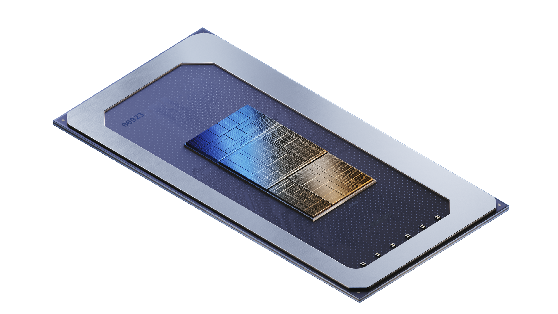
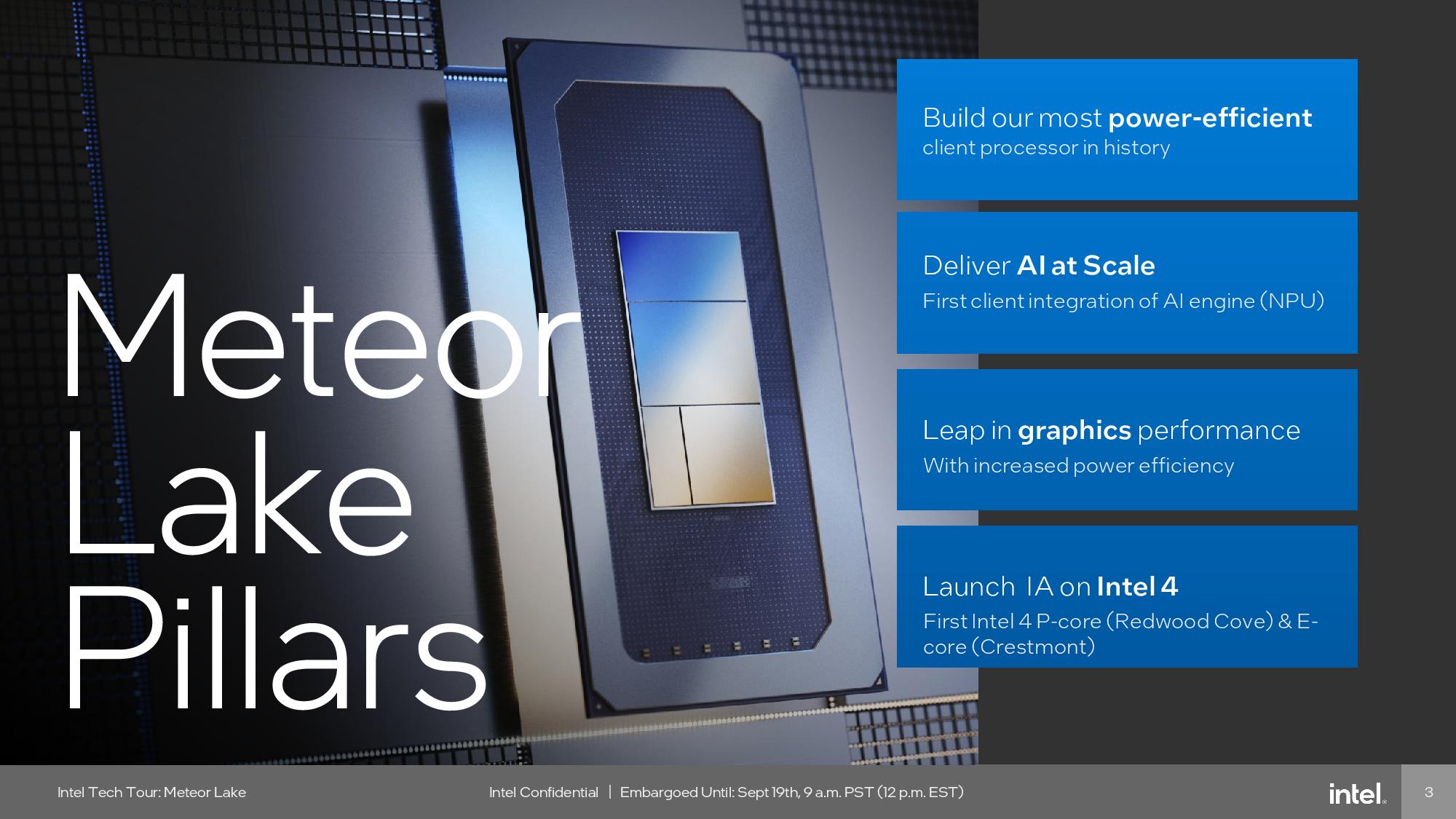
Intel shared the deep-dive details of its disruptive new Meteor Lake processors during its Intel Tech Tour in Malaysia, and while the company isn’t sharing product-level details yet, like the different chip models, before their launch on December 14, it’s whipping the covers off its new 3D performance hybrid architecture. That includes details about the chips’ CPU and GPU core microarchitectures, neural processing unit, Foveros 3D packaging that melds multiple chiplets into one chip, a new approach to power management, and its new low-power-island e-cores that create a third tier of CPU compute power in addition to the standard P-cores and E-cores. Intel also shared core details about its new EUV-enabled Intel 4 process node, which it says is delivering the best initial yields the company has seen in a decade.
Intel says its new design methodology results in stunning gains in power efficiency, but it hasn’t shared performance benchmarks yet. The company describes its move to Foveros 3D packaging technology as its largest architectural shift in 40 years, a fair statement given the radical new packaging technology will pave the way to more advanced chips in the future, with CEO Pat Gelsinger even calling it the company’s next ‘Centrino moment.’ These are needed changes as Intel looks to regain the lead over its primary fab competitor, TSMC, in process node tech, and outmaneuver its primary chip competitor, AMD, with its new chiplet-based architecture. Intel also has to fend off Apple, which has now made a disruptive entrance into the laptop market with faster, more power efficient processors.
Meteor Lake marks not only a fundamental rethinking of Intel’s processor design, but also its approach to fabricating its processors – these are the company’s first mainstream chips to use silicon from a competing fab. Intel leans on TSMC’s process node tech for three of the four active tiles on the processor, selecting two less expensive TSMC nodes for some functions, and one higher-density and higher-performance TSMC node than its own ‘Intel 4’ node that it uses for its CPU tile.
We’ll start at the top, covering the basic design elements, and then dive into the deeper details of each unit. We also have details of the overall AI implementation and software, along with the design decisions behind the new Foveros 3D-based architecture.
Intel Meteor Lake Architecture Overview
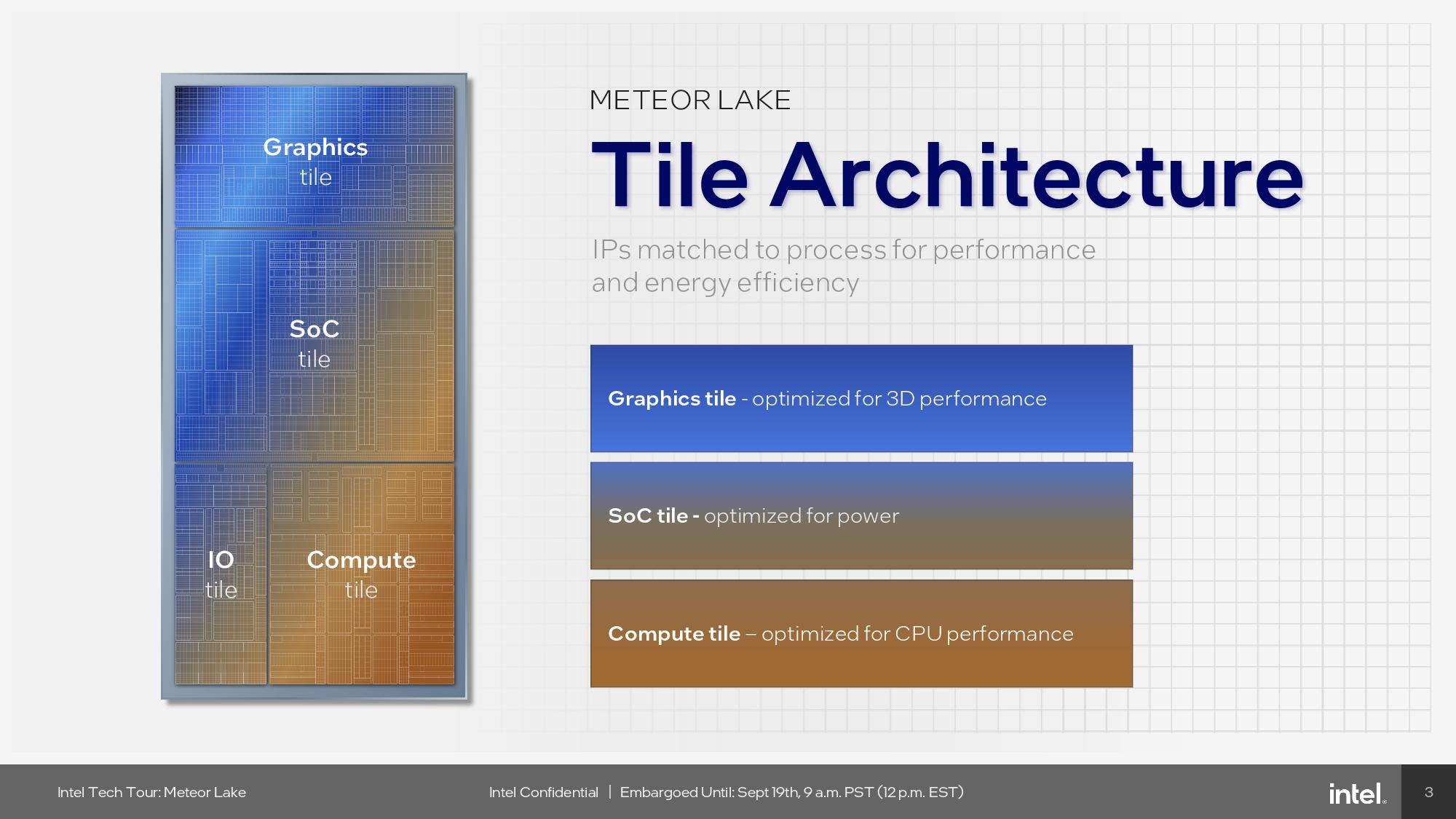
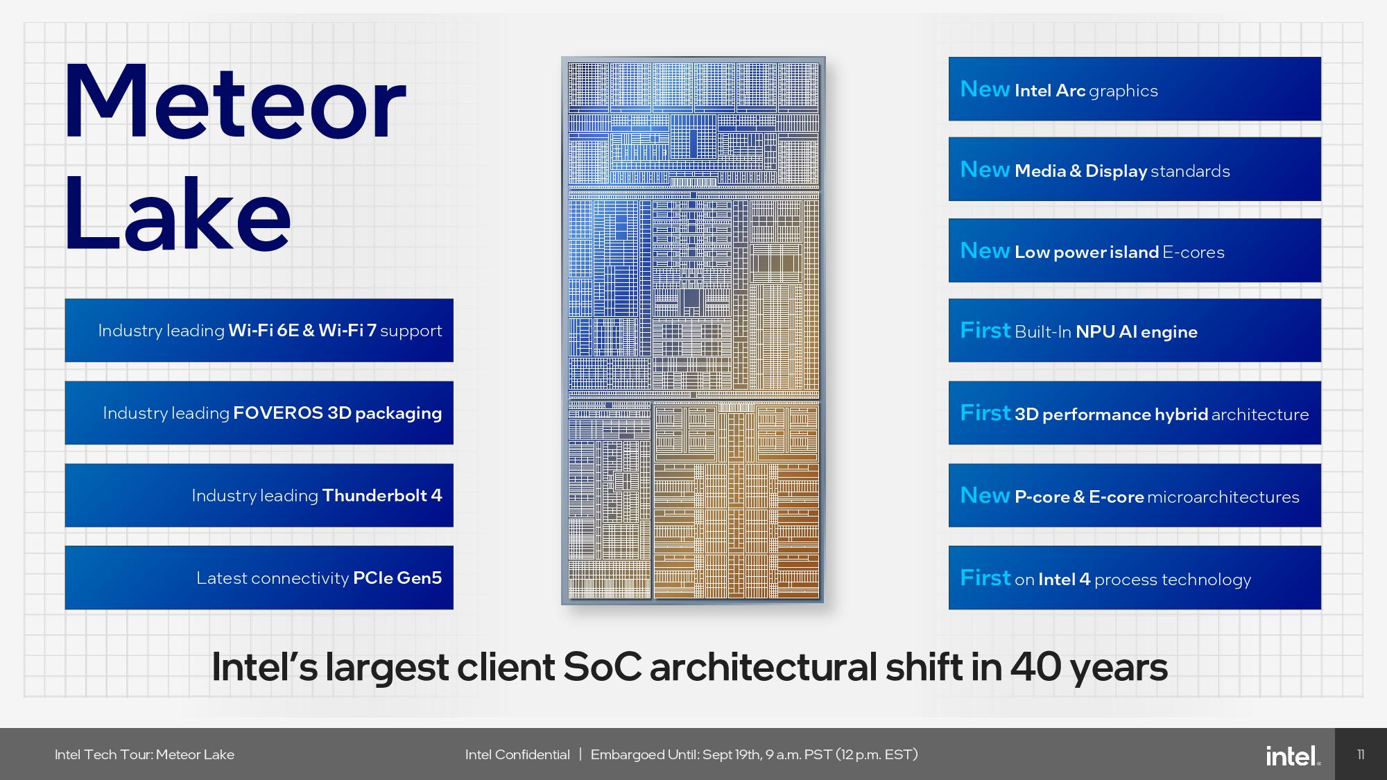




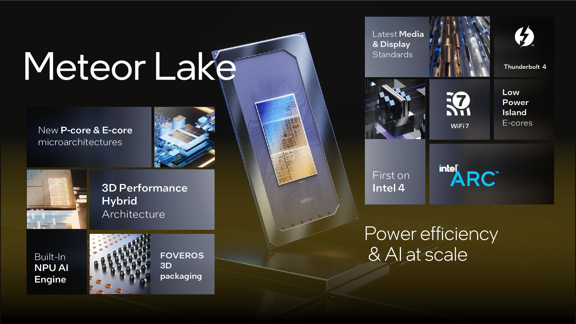
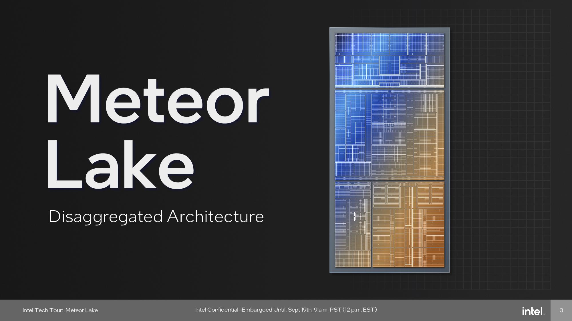
Intel refers to its die disaggregation technique as a ‘tiled’ architecture, whereas the rest of the industry refers to this as a chiplet architecture. In truth, there really isn’t much technical differentiation between the two terminologies. Intel says that a ‘tiled’ processor refers to a chip using advanced packaging, which enables parallel communication between the chip units, while standard packaging employs a serial interface that isn’t as performant or energy efficient. However, other competing processors with advanced packaging are still referred to as chiplet-based, so the terms are largely interchangeable.
| Intel Meteor Lake Tile/Chiplet | Manufacturer / Node |
| CPU Tile | Intel / 'Intel 4' |
| 3D Foveros Base Die | Intel / 22FFL (Intel 16) |
| GPU Tile (tGPU) | TSMC / N5 (5nm) |
| SoC Tile | TSMC / N6 (6nm) |
| IOE Tile | TSMC / N6 (6nm) |
Meteor lake has four disaggregated active tiles mounted atop one passive interposer: a Compute (CPU) tile, graphics (GPU) tile, SoC tile, and I/O tile. All these units are Intel-designed and feature Intel microarchitectures, but external foundry TSMC will manufacture the I/O, SoC, and GPU tiles, while Intel manufactures the CPU tiles on its Intel 4 process. All four of these active tiles ride on top of a single unifying Intel-produced Foveros 3D base tile that ties together the functional units with high enough bandwidth and low enough latency for the chip to function as close to one monolithic die as possible.
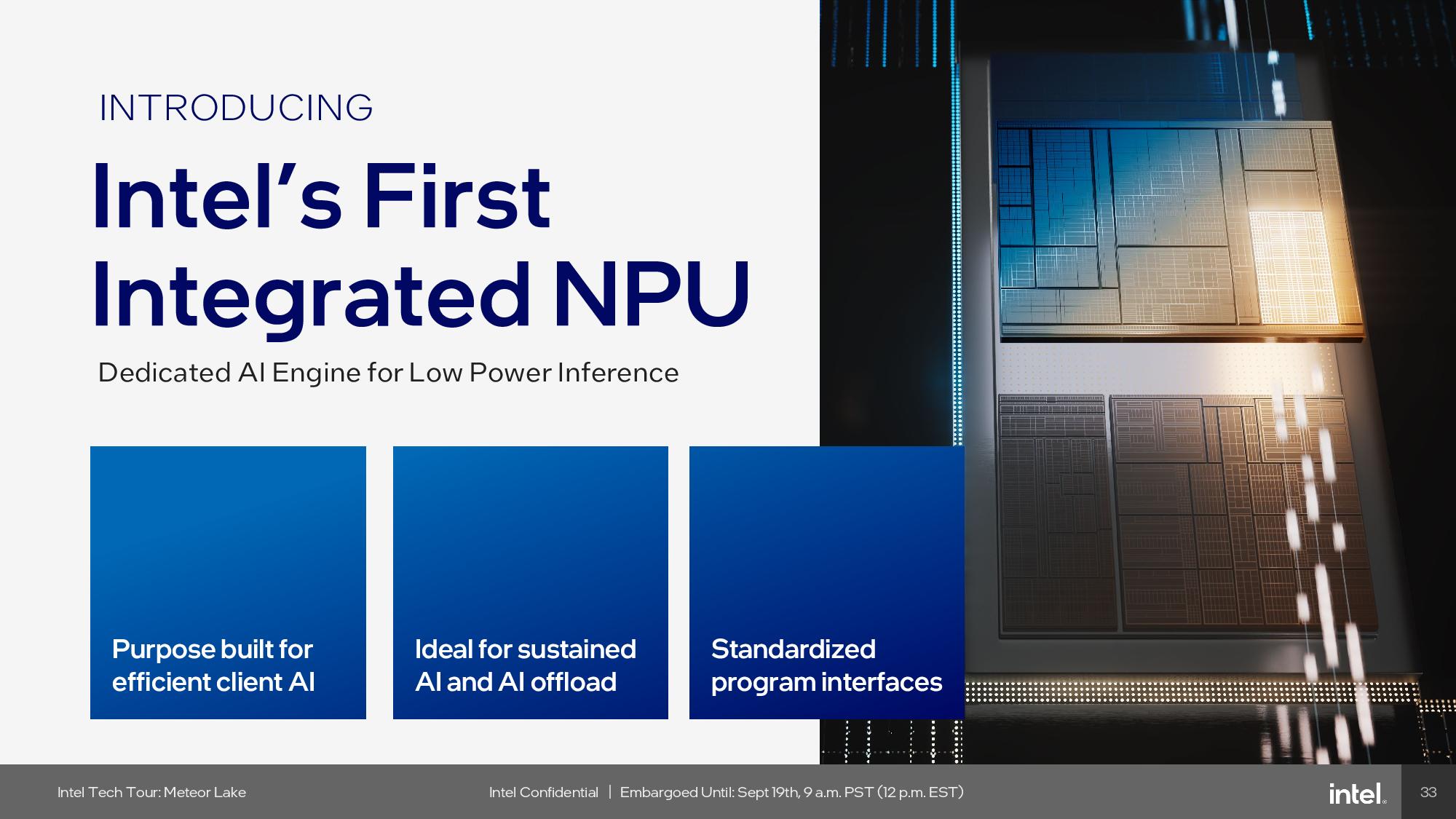
All told, Meteor Lake has three compute units that can process AI workloads, the CPU, NPU and GPU. AI workloads will be directed to each unit based on workload requirements, which we’ll dig into a bit further below.
Get Tom's Hardware's best news and in-depth reviews, straight to your inbox.
Meteor Lake Compute (CPU) Tile
Intel fabs its compute (CPU) tile with the Intel 4 process, which it selected because it affords opportunities for tightly tuning its process node for the specific requirements of a high-powered CPU. We’ll dive into the details of the Intel 4 node later in the article.
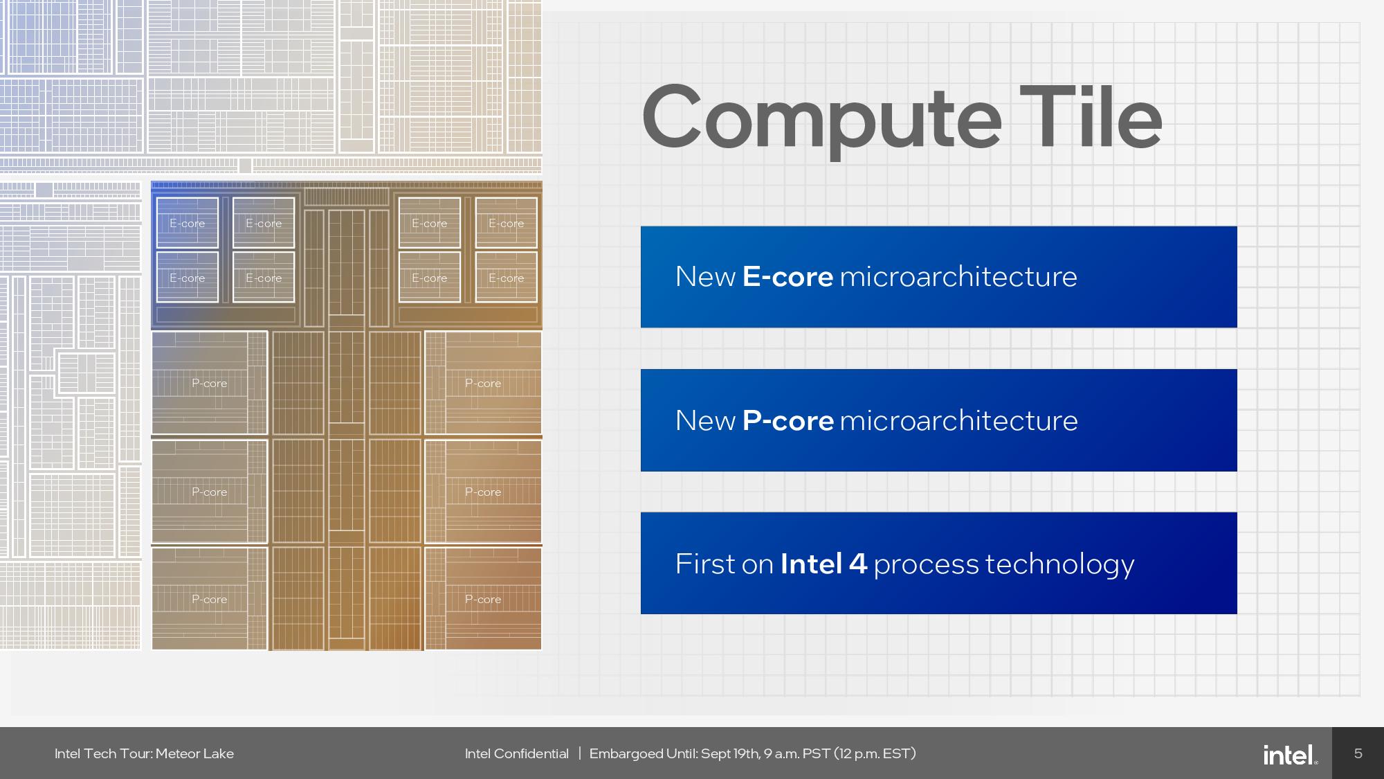
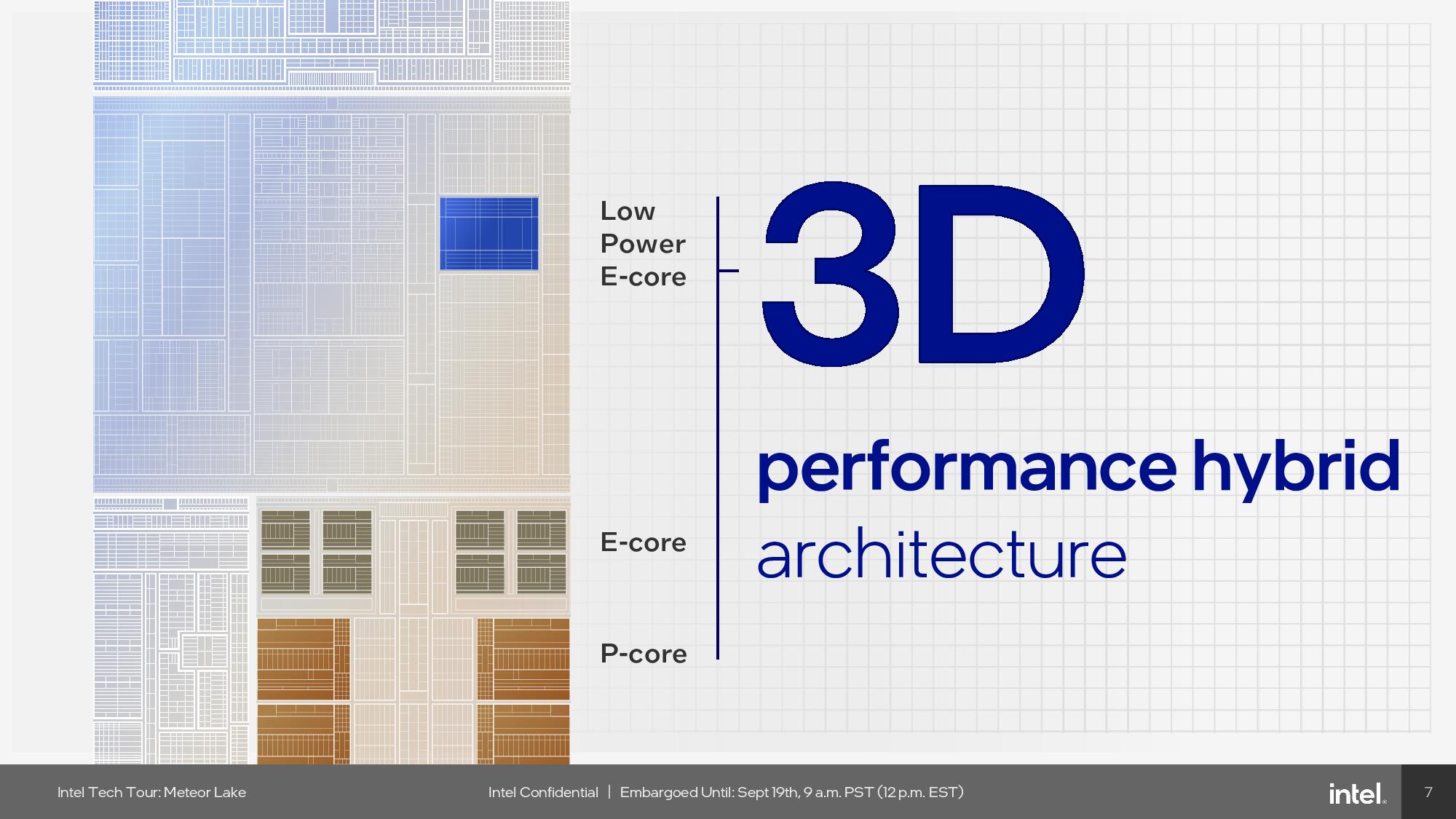
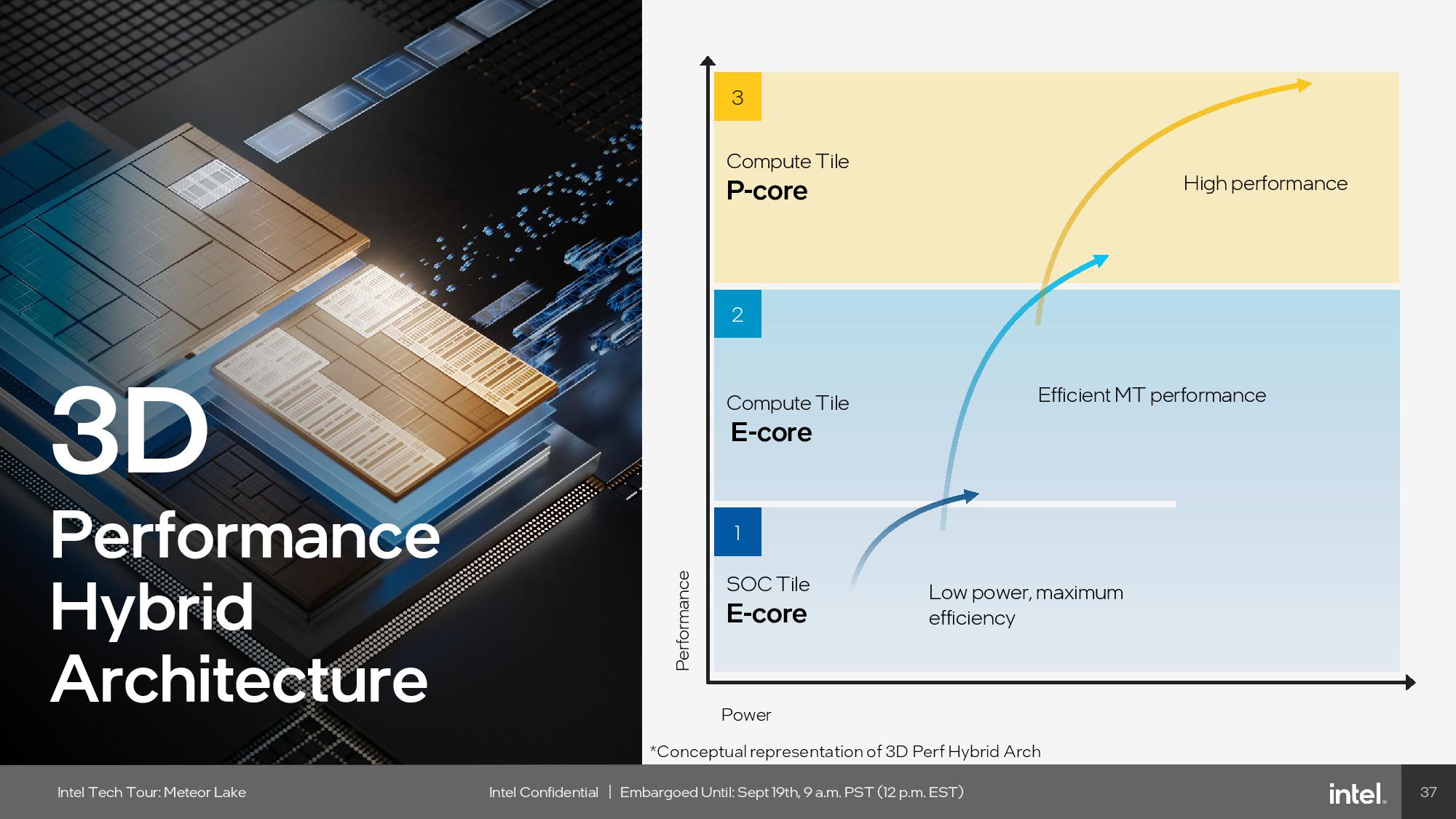
As before, Intel has a mixture of P-core and E-cores, with P-cores handling latency sensitive single-threaded and multi-threaded work, while the E-cores step in to handle both background and heavily threaded tasks. However, these two types of cores are now augmented by two new low-power-island e-cores located on the SoC tile. These two new cores are geared for the lowest-power tasks, which we’ll cover in the SoC tile section below. Intel calls this new three-tier core hierarchy the 3D performance hybrid architecture.
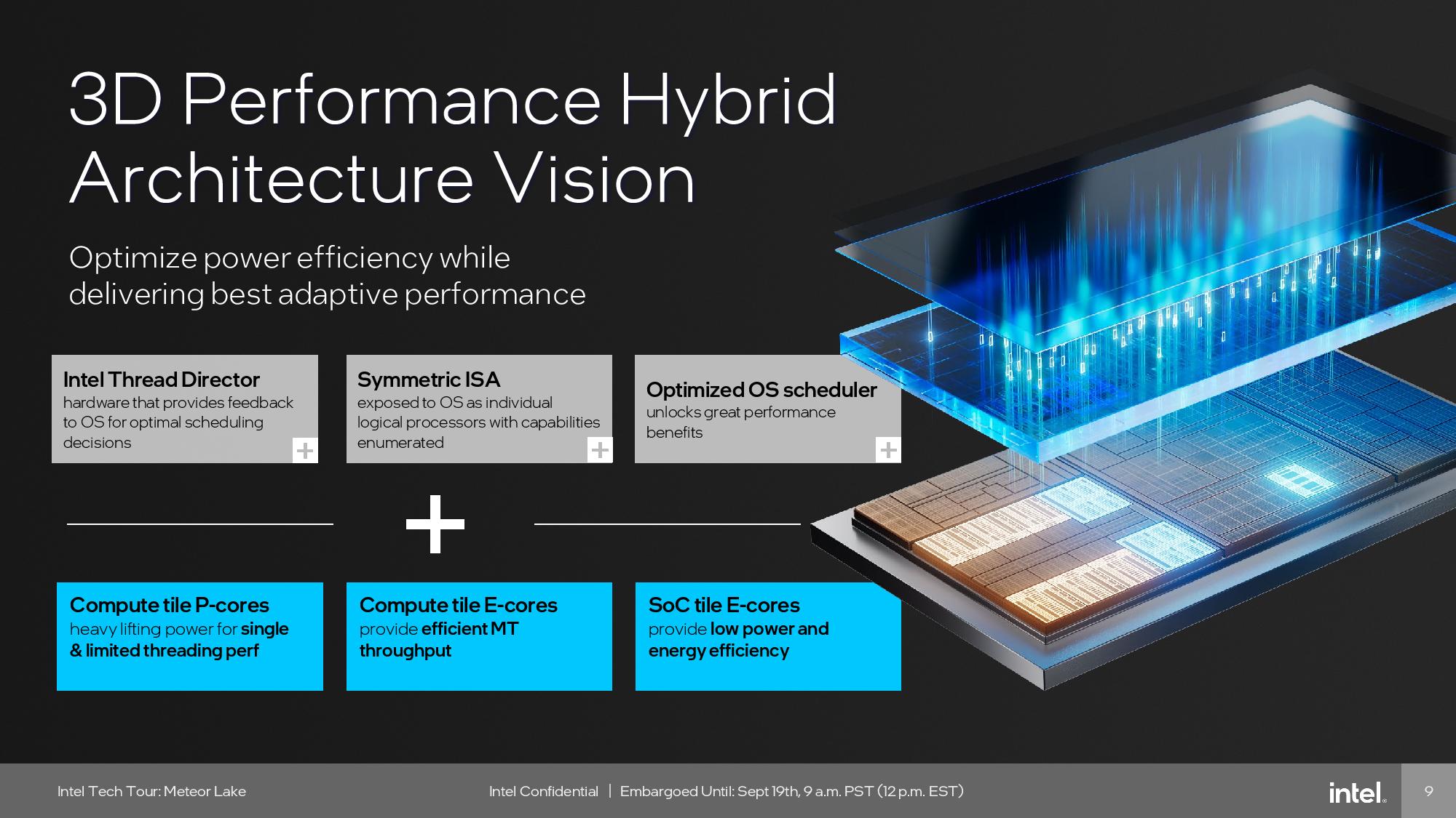
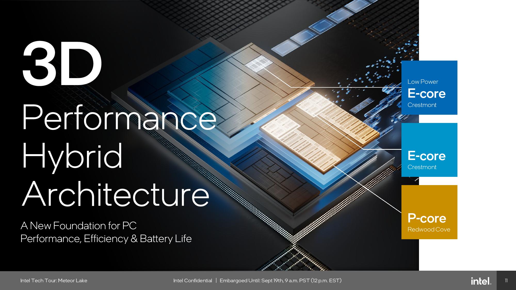
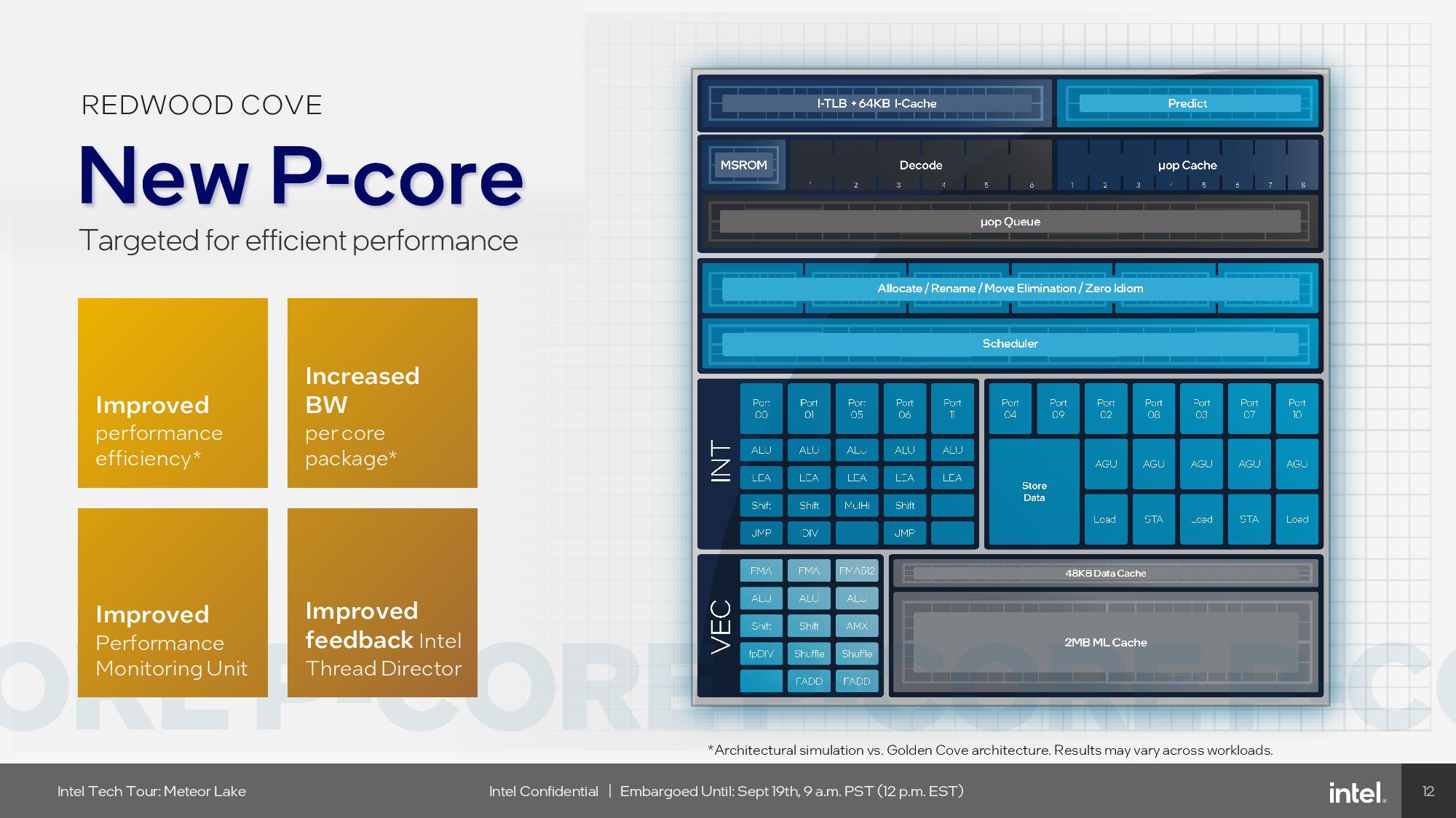

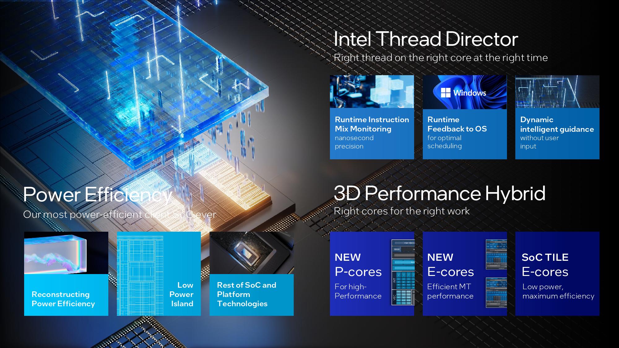
The compute tile carries the Redwood Cove P-Cores and Crestmont E-cores, and surprisingly, there aren’t many IPC improvements to speak of. In fact, while the Redwood Cove cores do have some improvements under the hood, they don’t provide an improvement in instructions per clock (IPC) throughput. Intel says Redwood Cove is akin to what it has traditionally called a ‘tick,’ meaning its basically the same microarchitecture and IPC as found in the Golden Cove and Raptor Cove microarchitectures used with the 12th and 13th generation Alder/Raptor Lake processors.
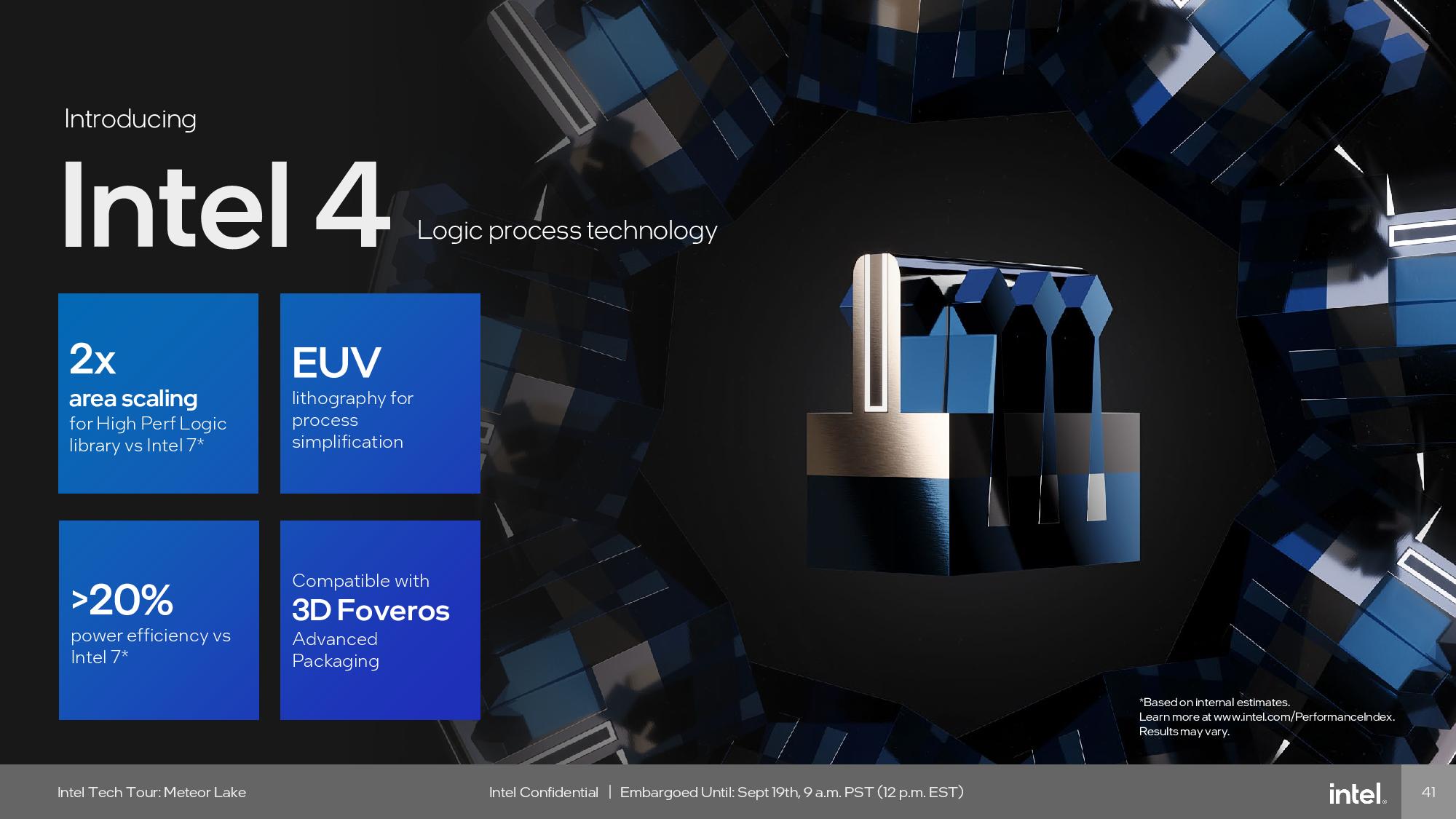
With a tick, instead of relying upon microarchitectural IPC gains, Intel instead uses a proven architecture to unlock the advantages of a more refined and smaller process; in this case, Intel 4. The new Intel 4 process does provide better performance at any given point on the voltage/frequency curve than the Intel 7 node previously used in Intel’s PC chips, meaning it can either run faster at the same power level, or run at the same speed with lower power. Intel says it focused on extracting higher power efficiency with this design, so it’s clear that we shouldn’t expect radical performance gains from the P-cores. Intel does say the Intel 4 process confers a 20% improvement in power efficiency, which is impressive.
Intel did do some plumbing work to accommodate the new tiled design, like improving the memory and cache bandwidth both on a per-core and package level, which could result in an extra bit of improvement in multi-threaded workloads. It also added enhanced telemetry data for its power management unit, which helps improve power efficiency and generate better real-time data that’s fed to the Thread Director, thus ensuring the correct workloads are placed on the correct cores at the right time.
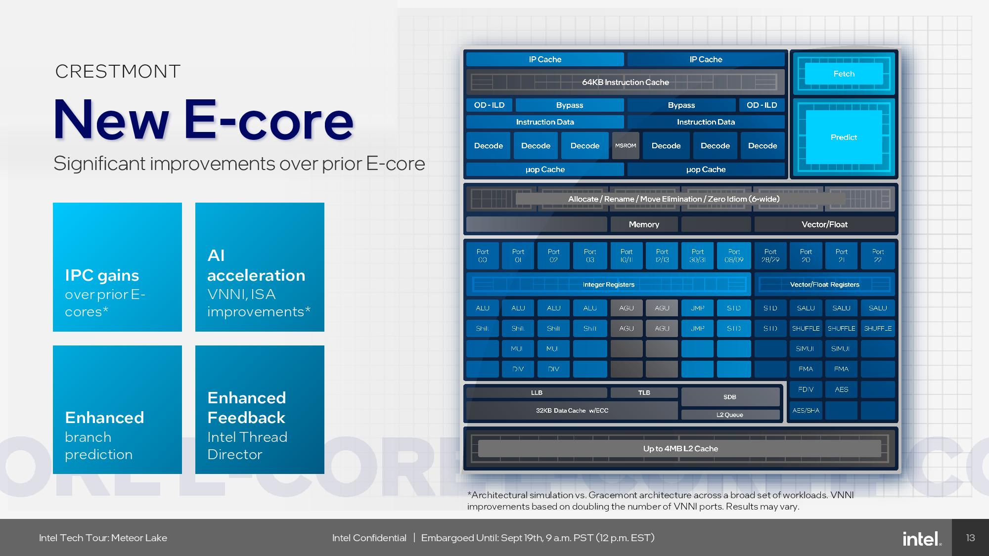
Intel’s Crestmont E-Core microarchitecture does have a 3% IPC improvement over the previous-gen Gracemont, but much of that stems from the addition of support for Vector Neural Network Instructions (VNNI) instructions that boost performance in AI workloads. Intel also made unspecified improvements to the branch prediction engine.
Crestmont does have one major new advance, though: This Crestmont architecture supports arranging the e-cores into either two or four-core clusters that share a 4MB L2 cache slice and 3MB of L3 cache. The previous-gen Gracemont didn’t have that capability, so Intel could only use e-cores in four-core clusters. Now Intel can carve out smaller dual-e-core clusters with twice the amount of cache per core, and that’s exactly the approach it took for the low-power-island e-cores on the SoC tile – those cores use the same Crestmont architecture as the standard e-cores on the compute die, but they are tuned for the TSMC N6 process node.
As with prior generations, each E-core is single-threaded. Intel also doubled the L1 cache to 64KB and employs a 6-wide decode engine (dual 3-wide to improve latency and power consumption), 5-wide allocate, and 8-wide retire.
The Crestmont cores do not support AMX or AVX-512, but they do not support AVX10. [EDIT 9/22/2023: Corrected article to reflect that Meteor Lake does not support AVX10.]
Meteor Lake Graphics (GPU) Tile
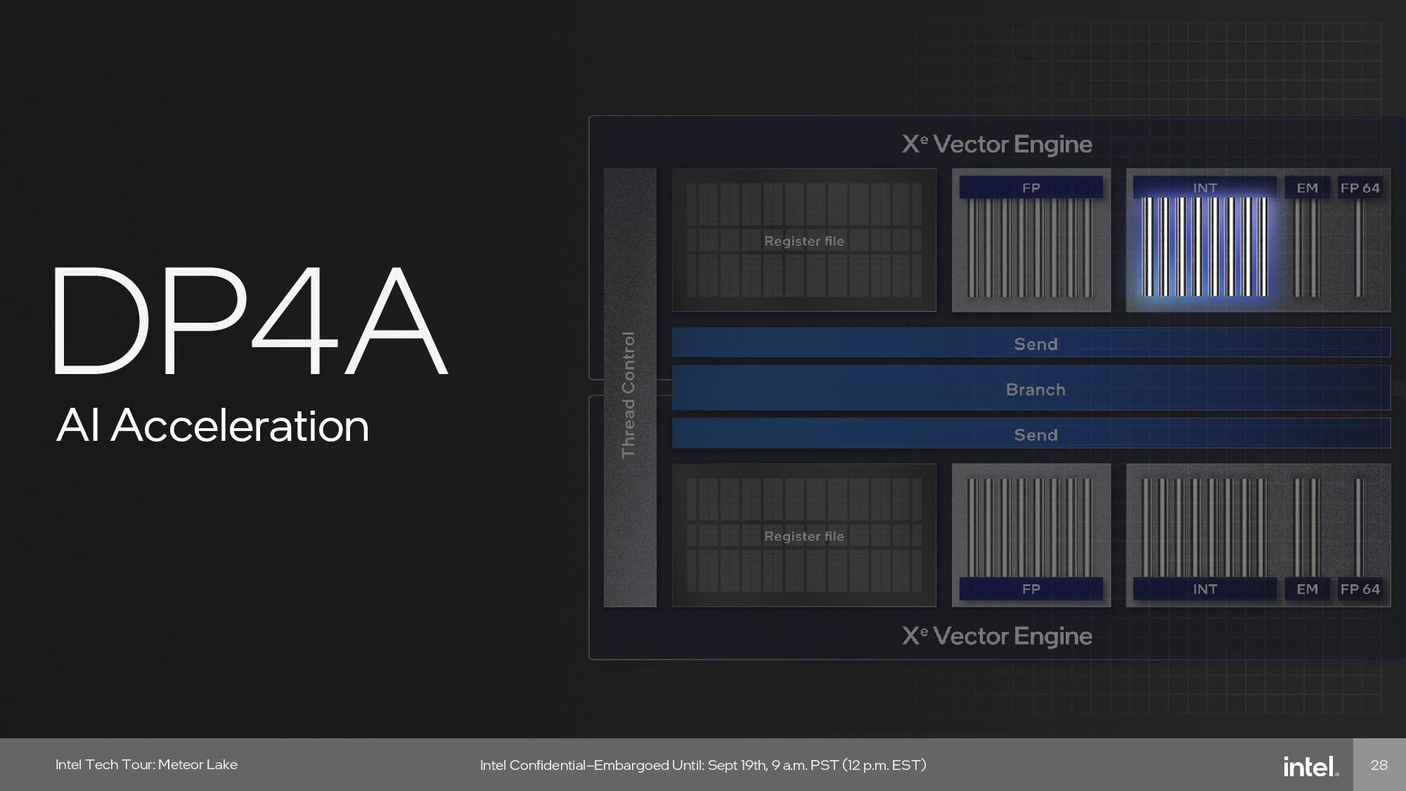
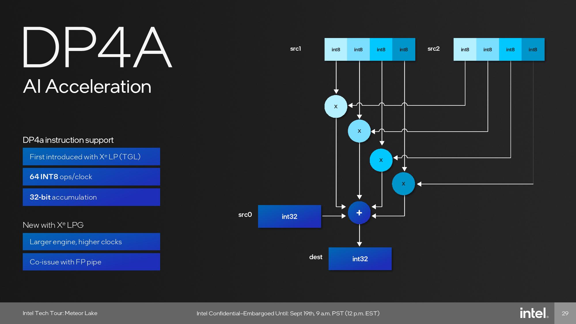

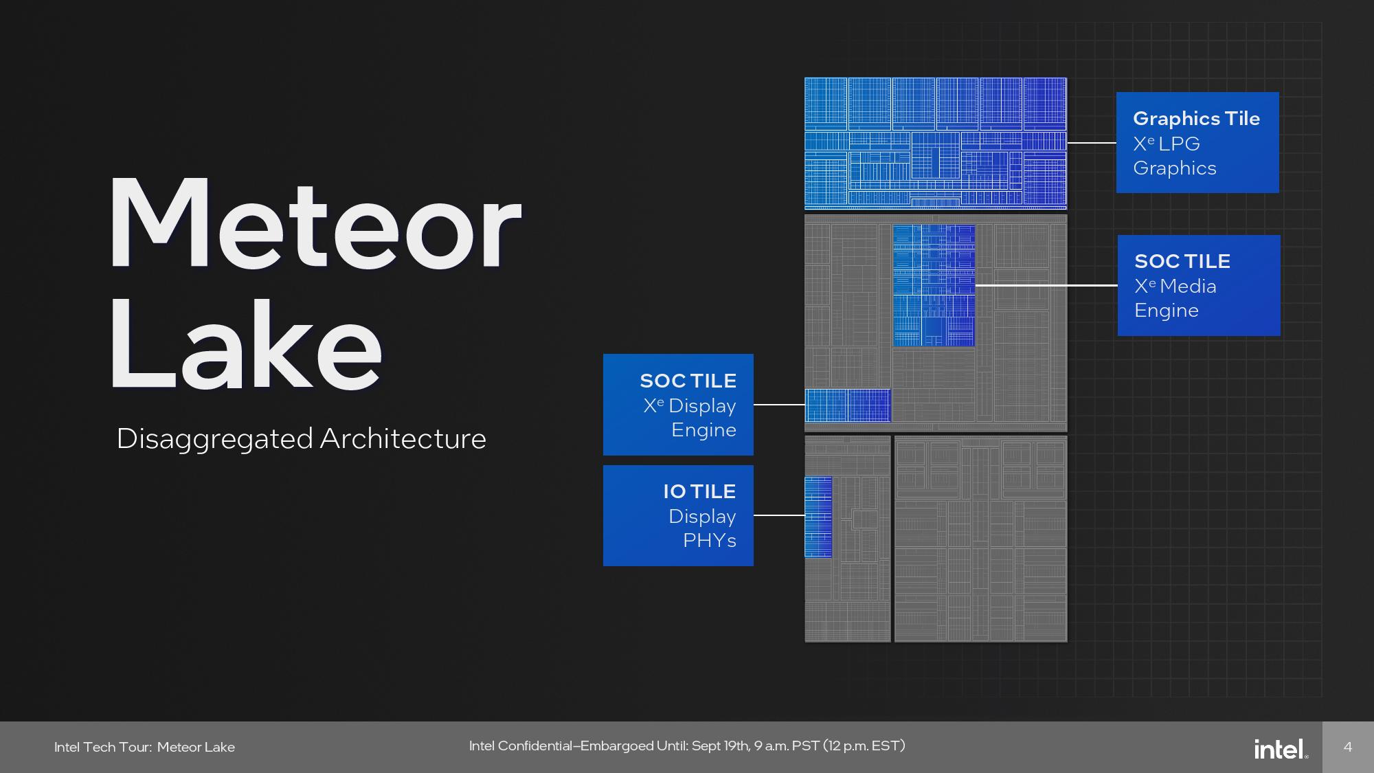
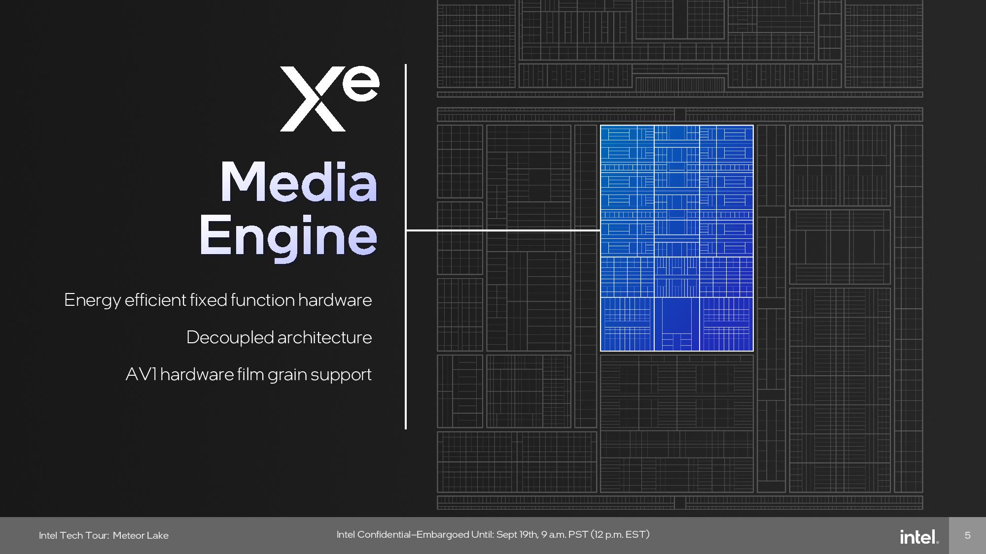
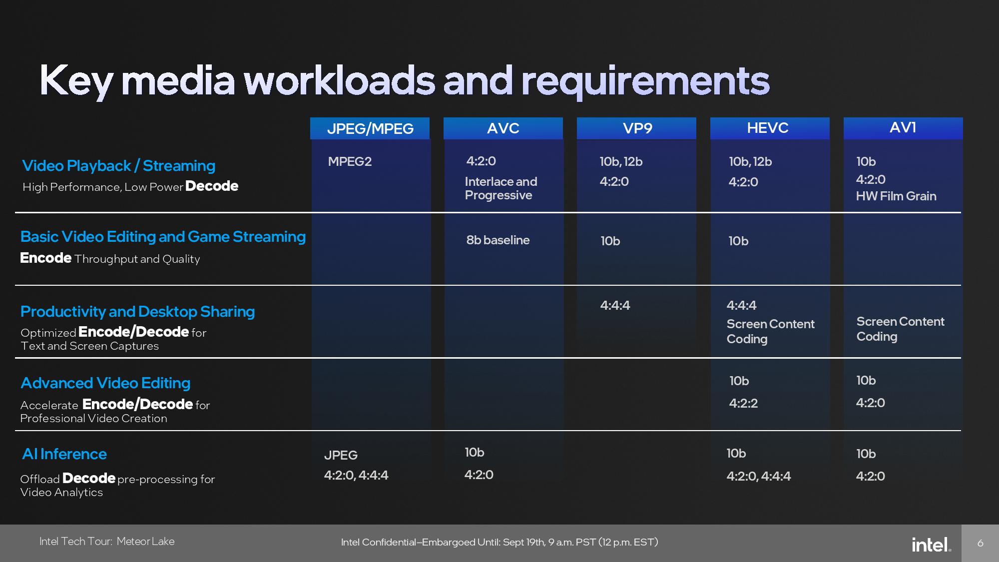
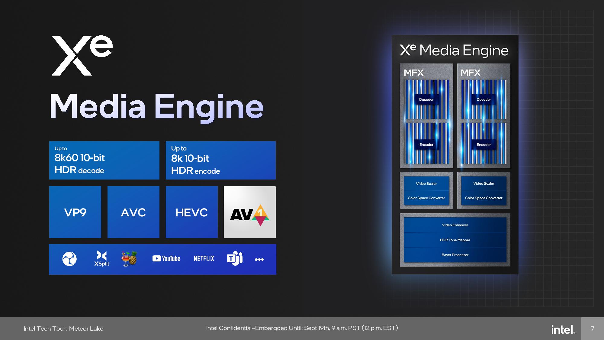
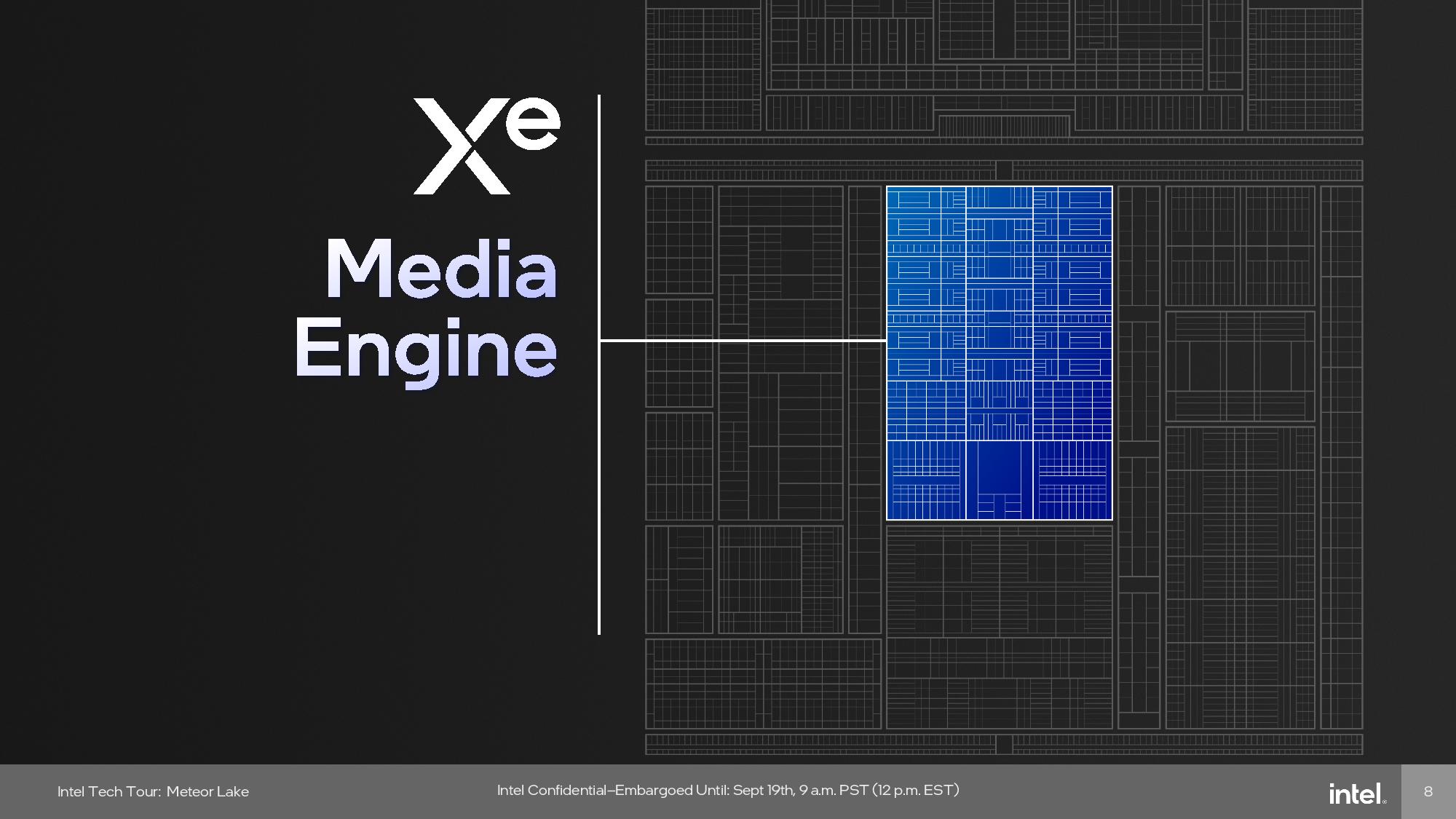
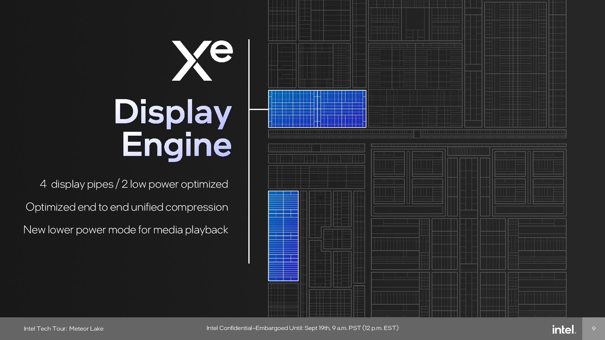
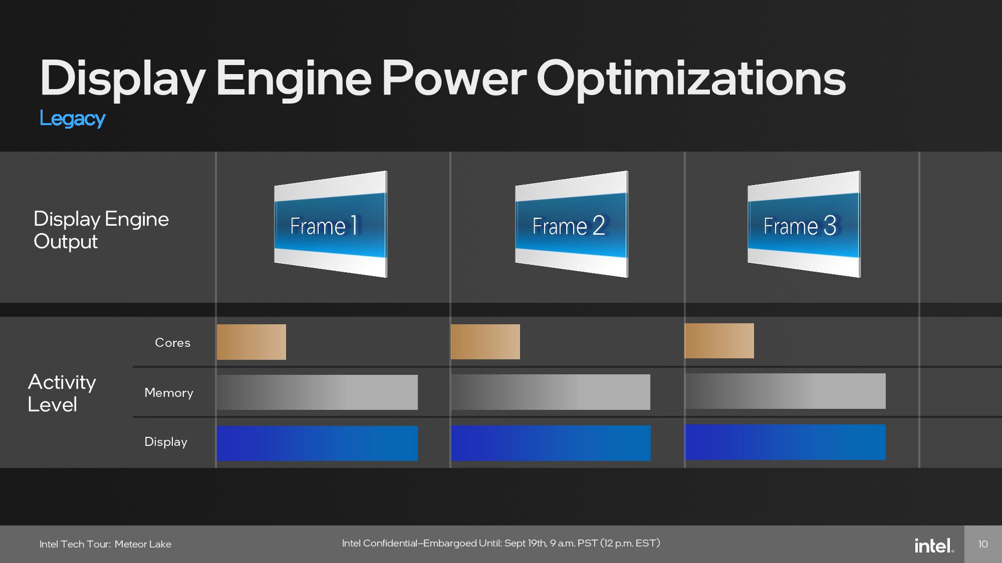
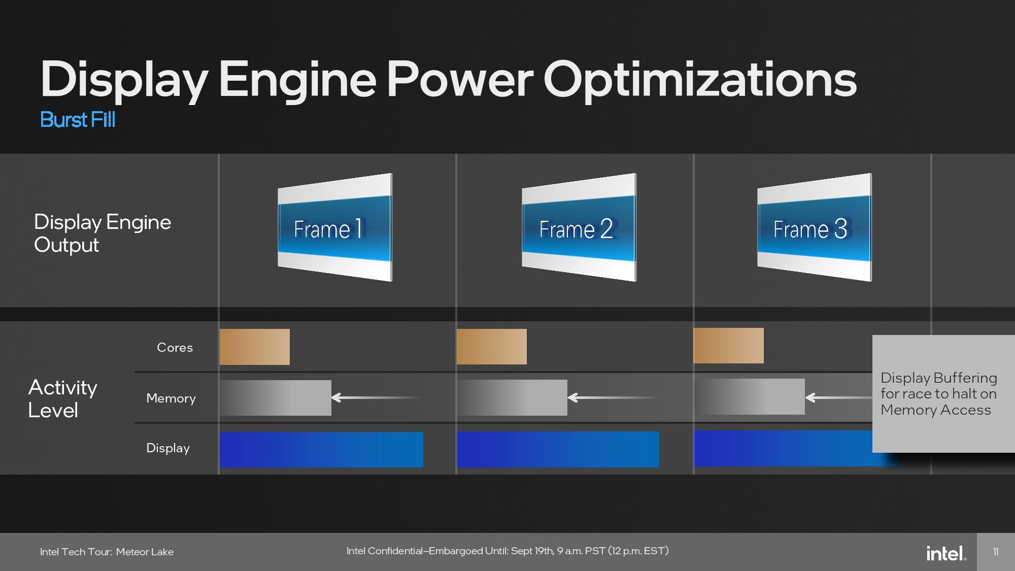
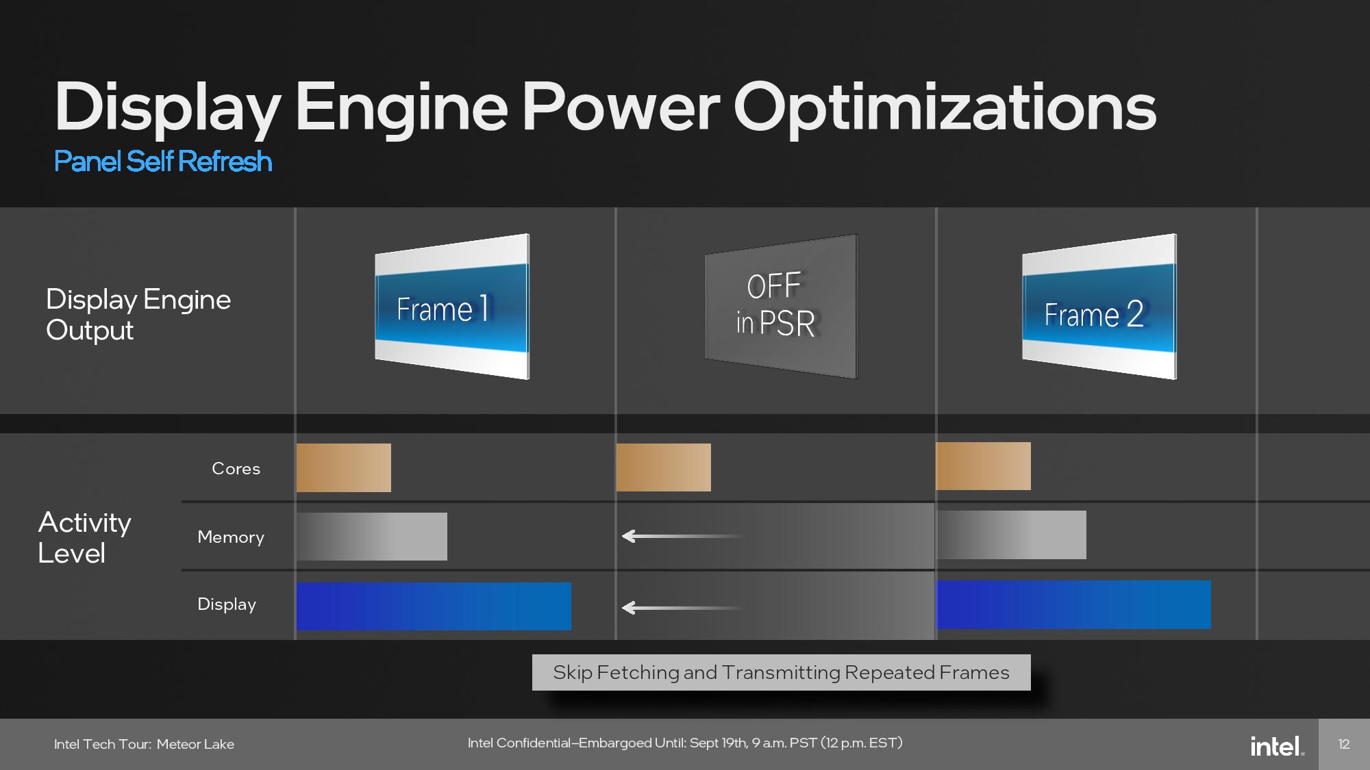
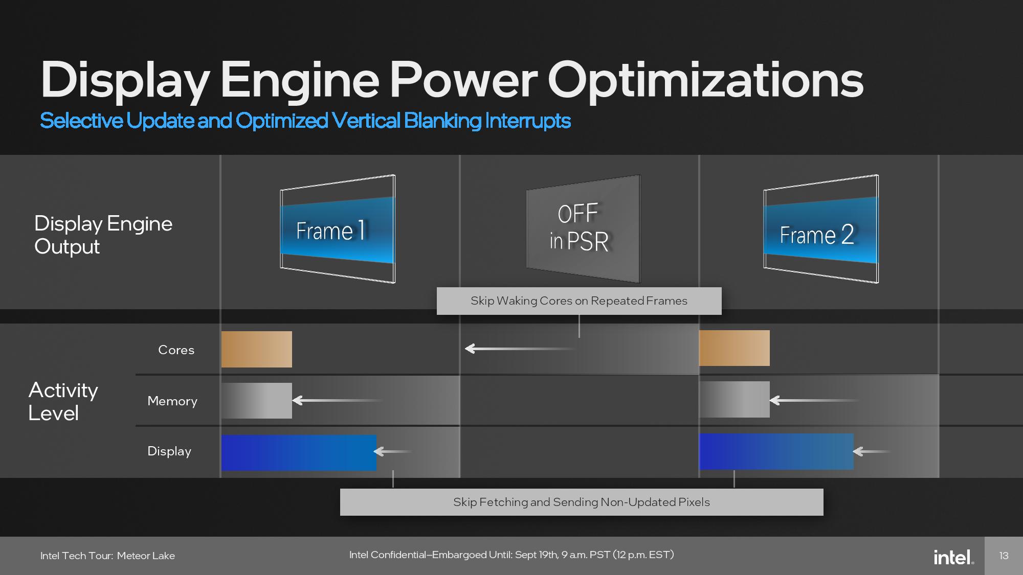
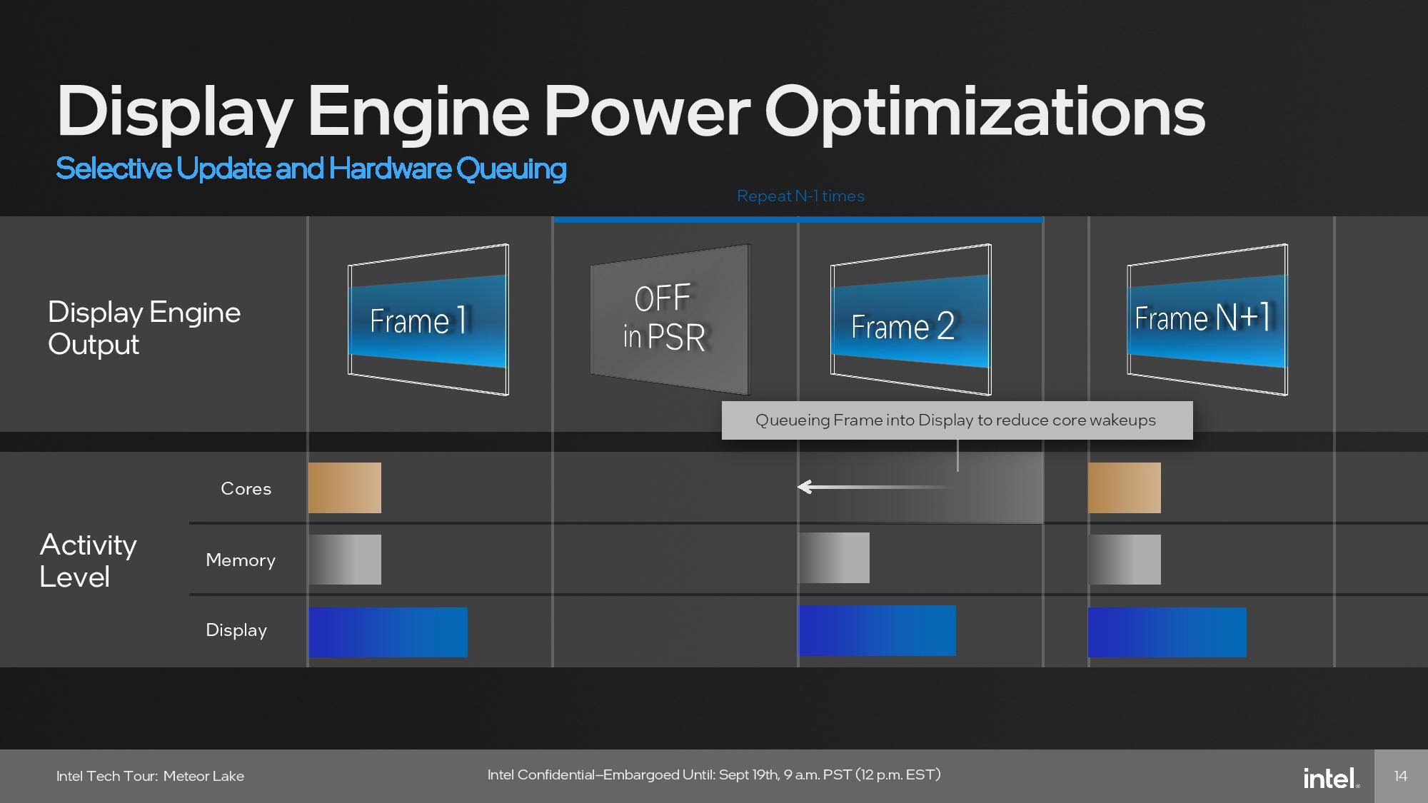
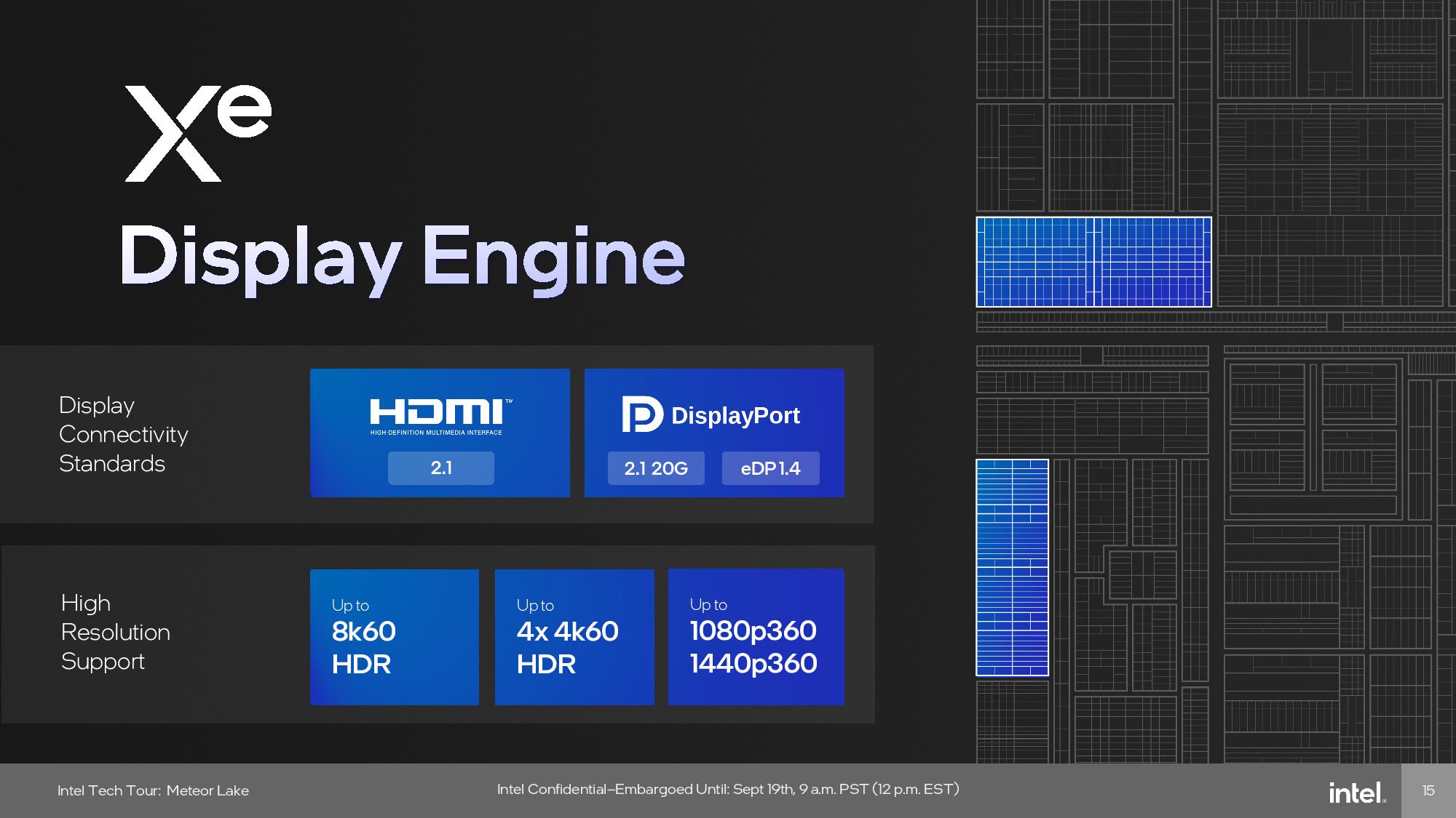
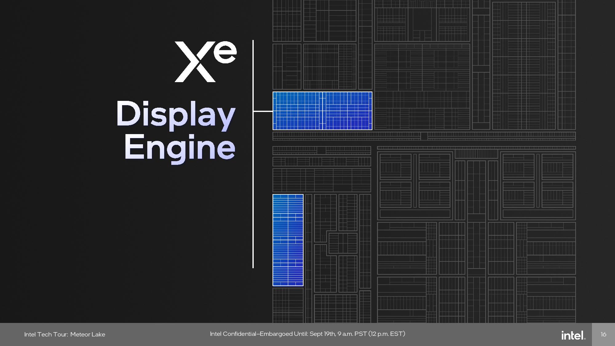
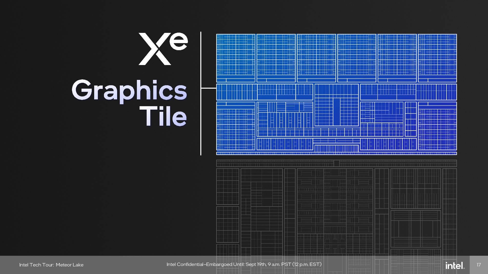
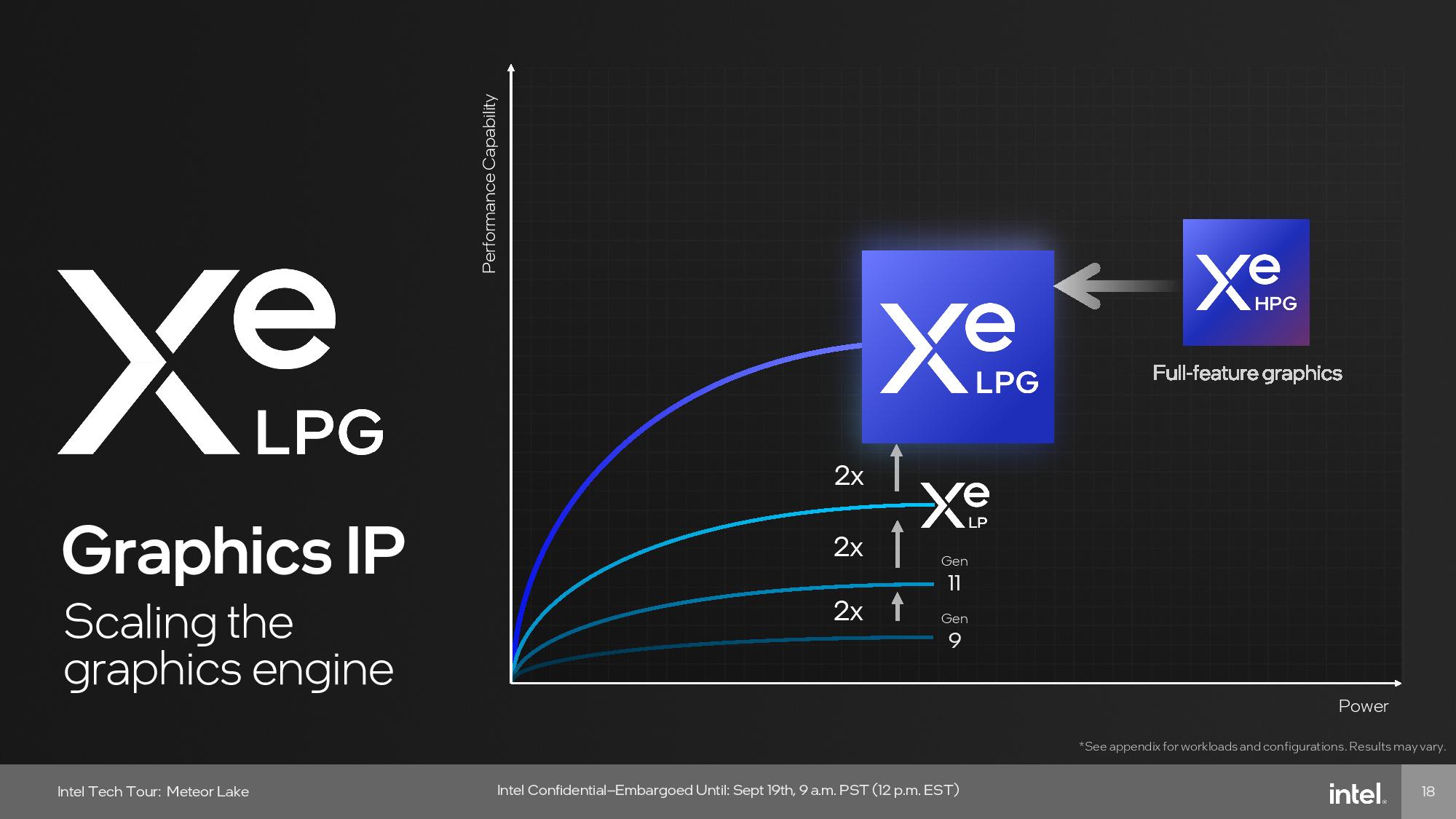
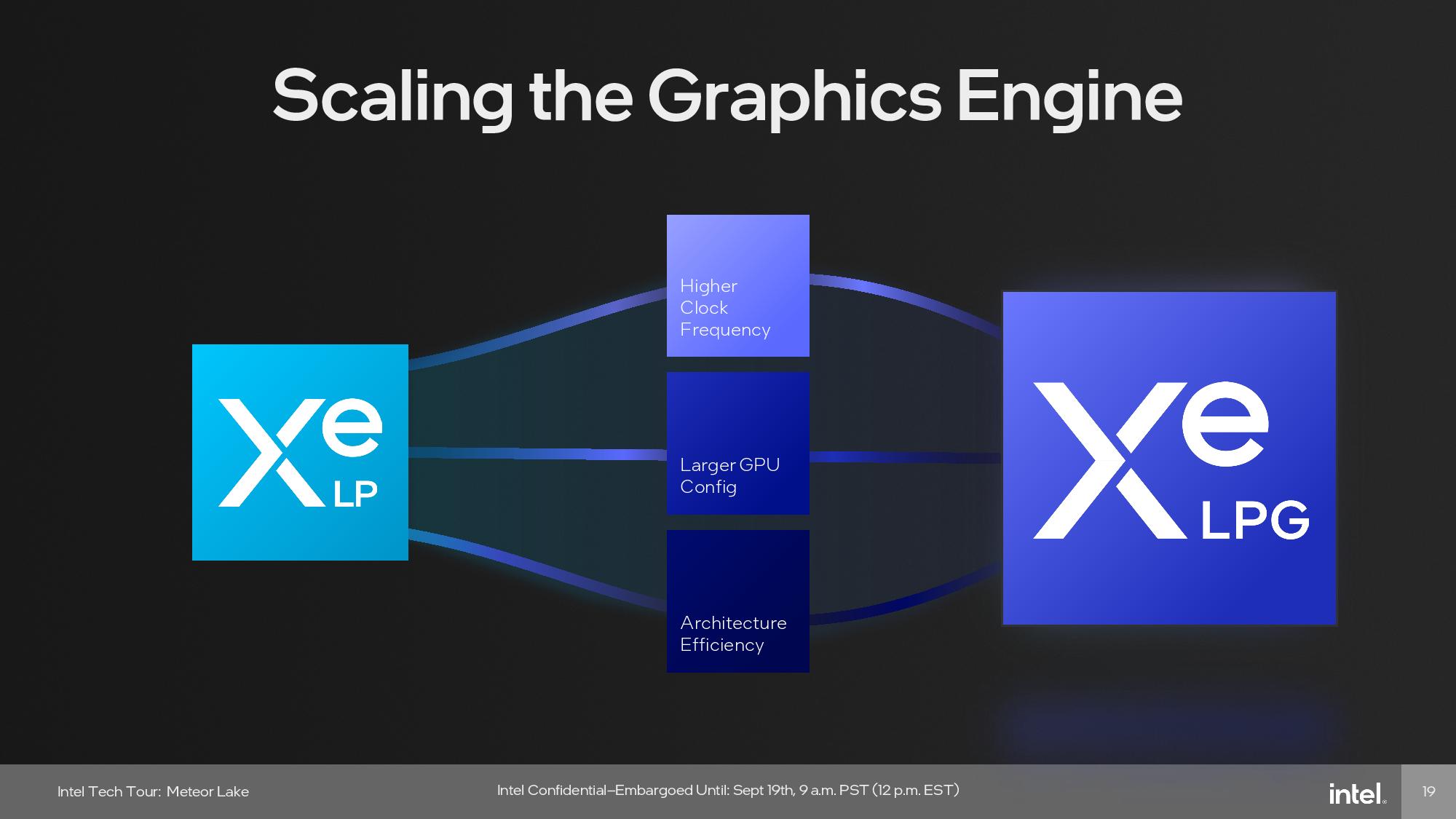
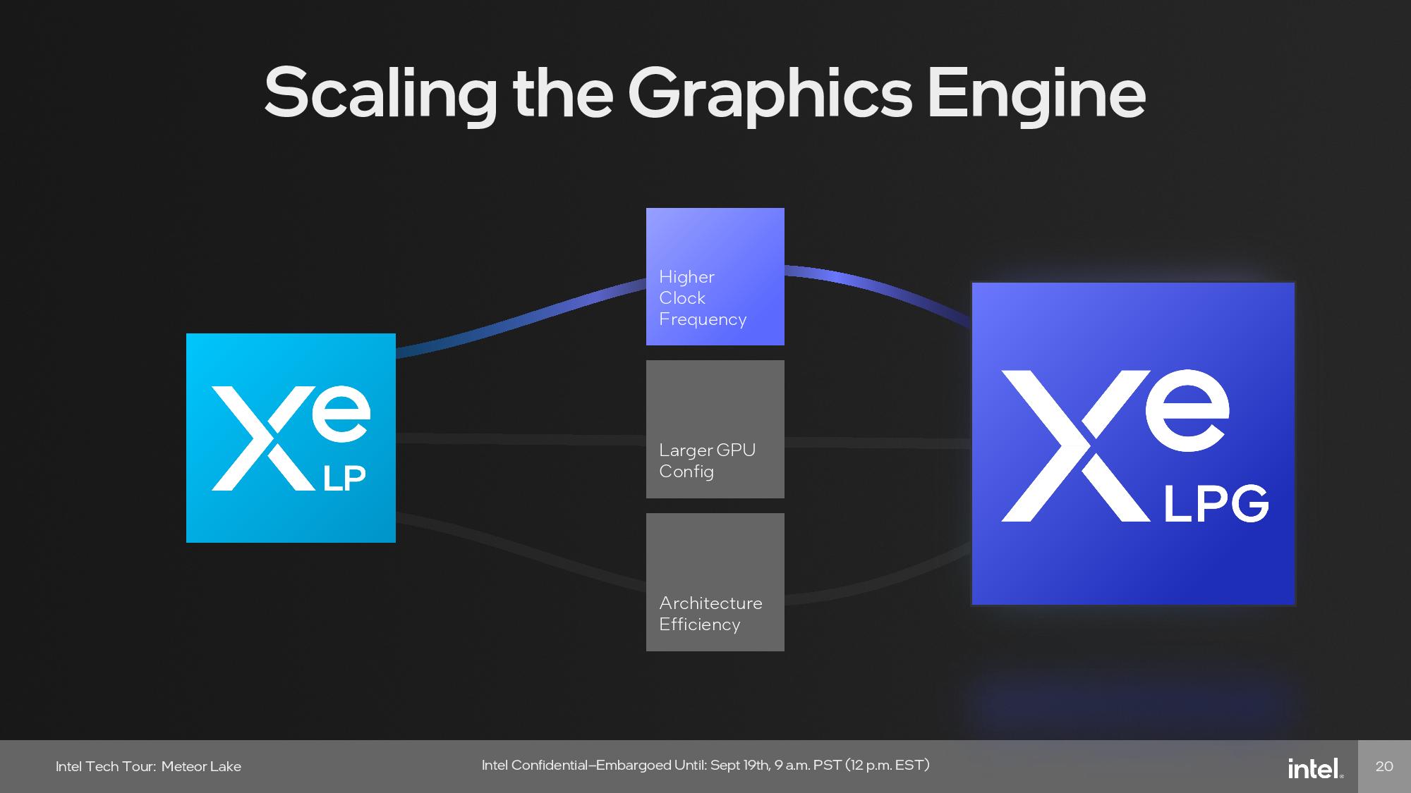
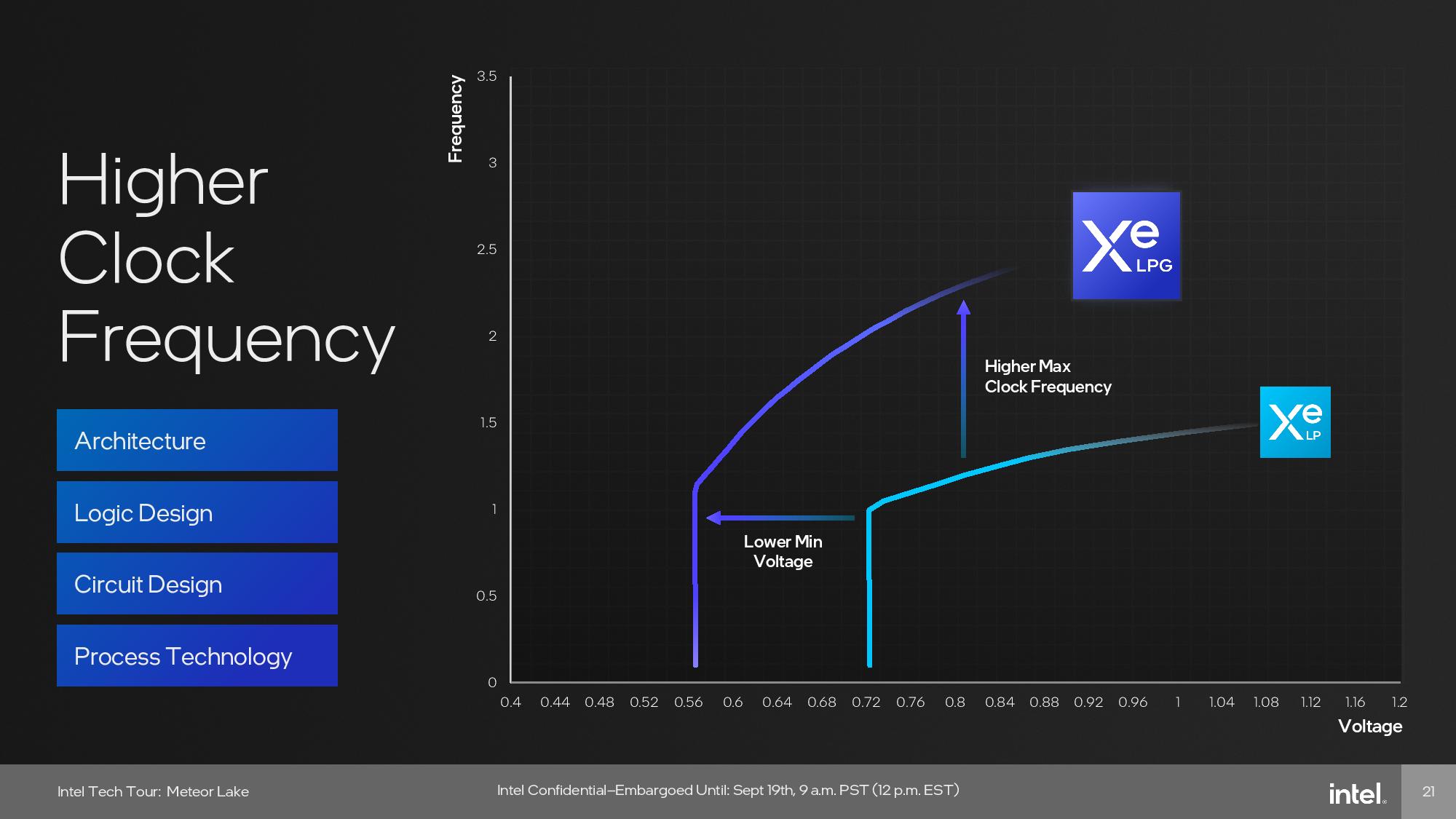
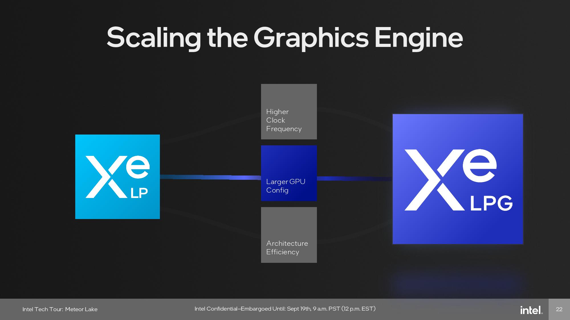
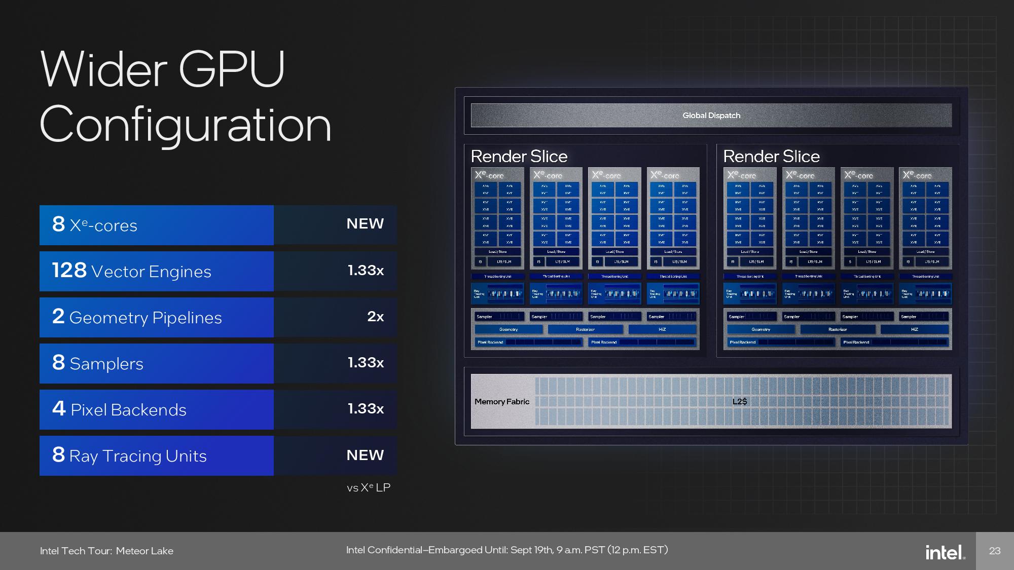
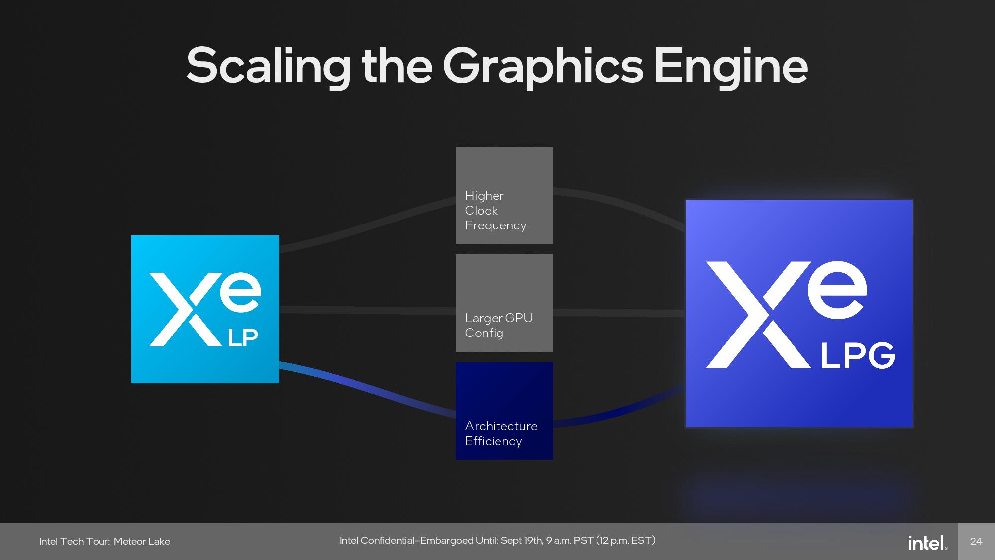
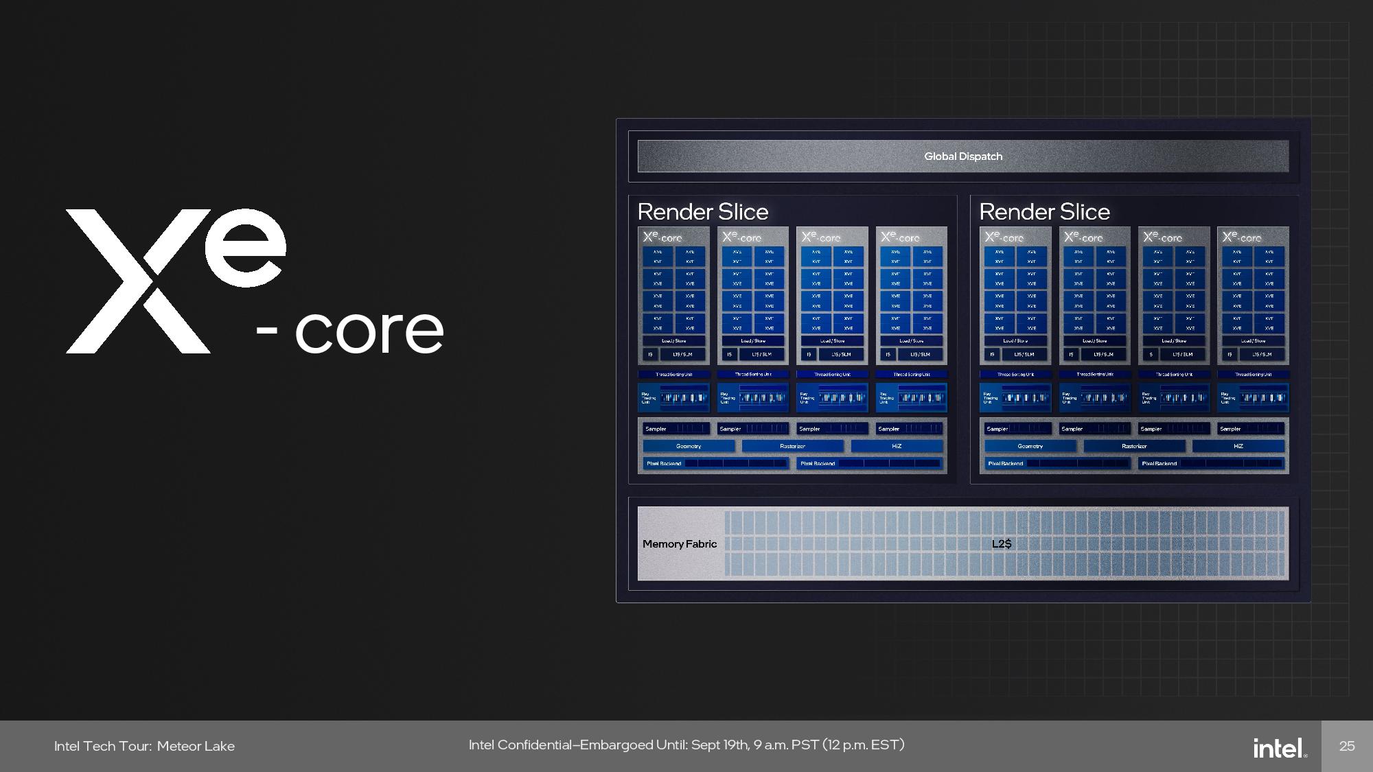
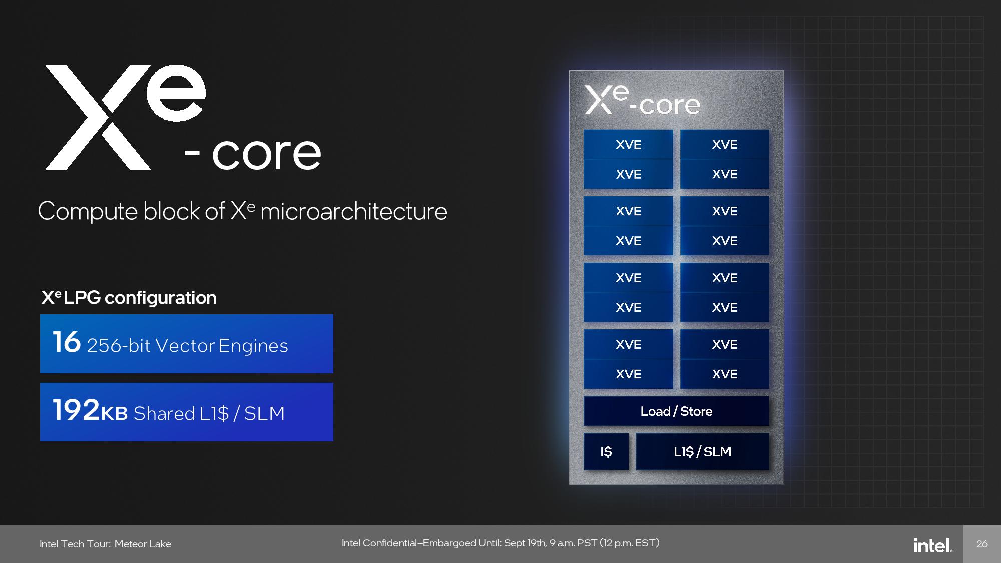
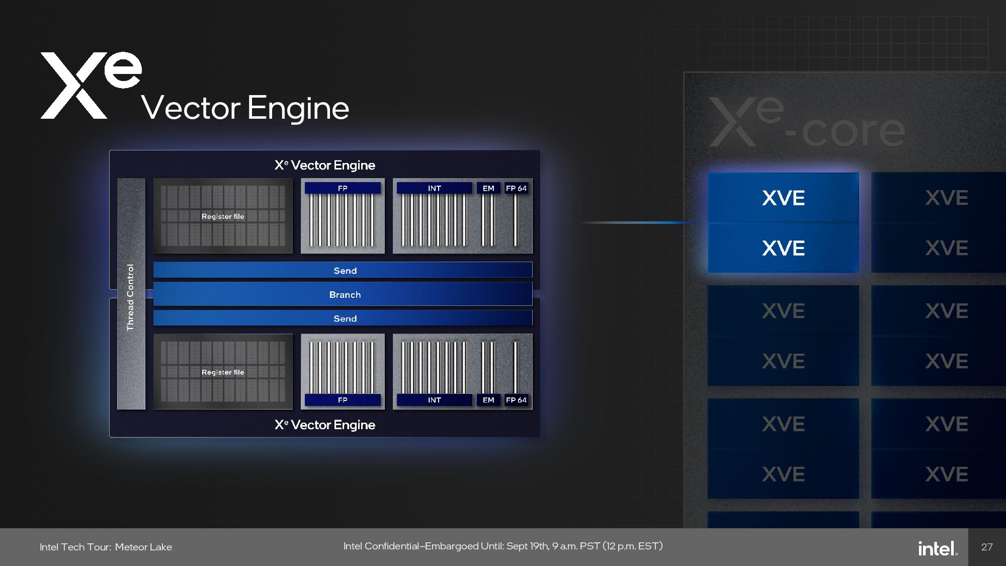
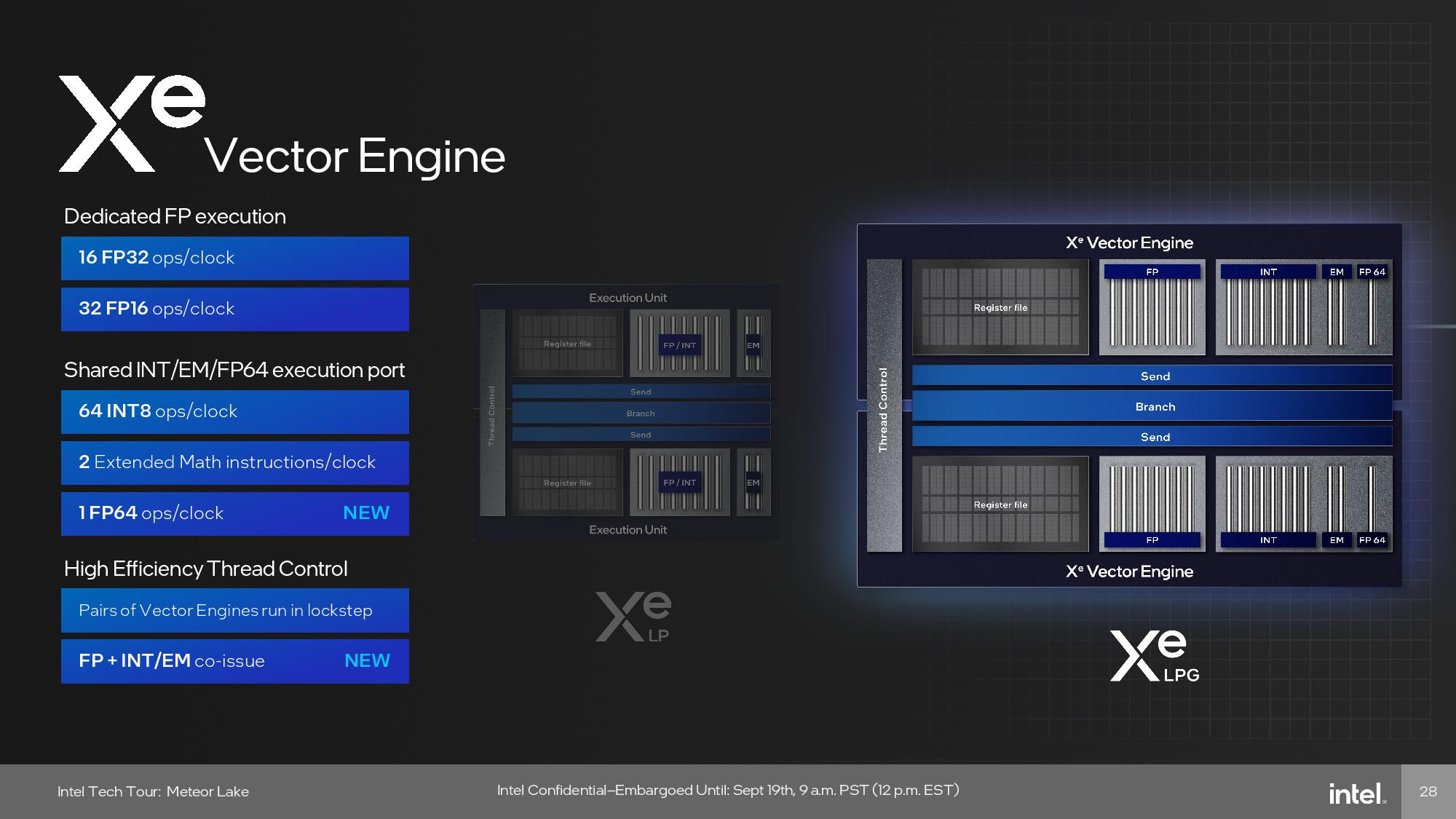
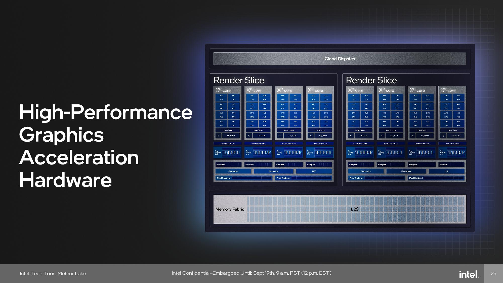
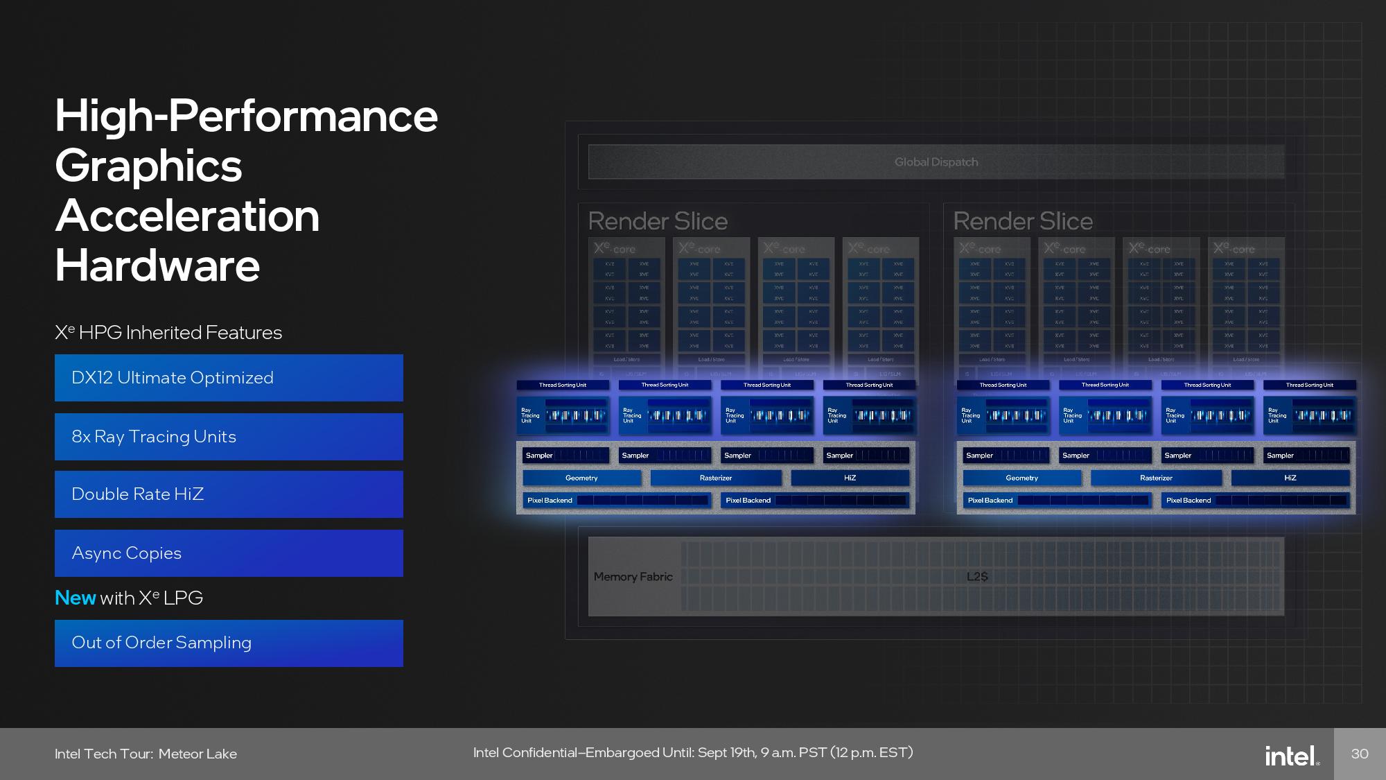
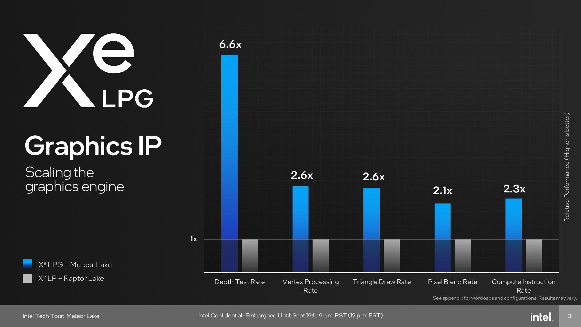
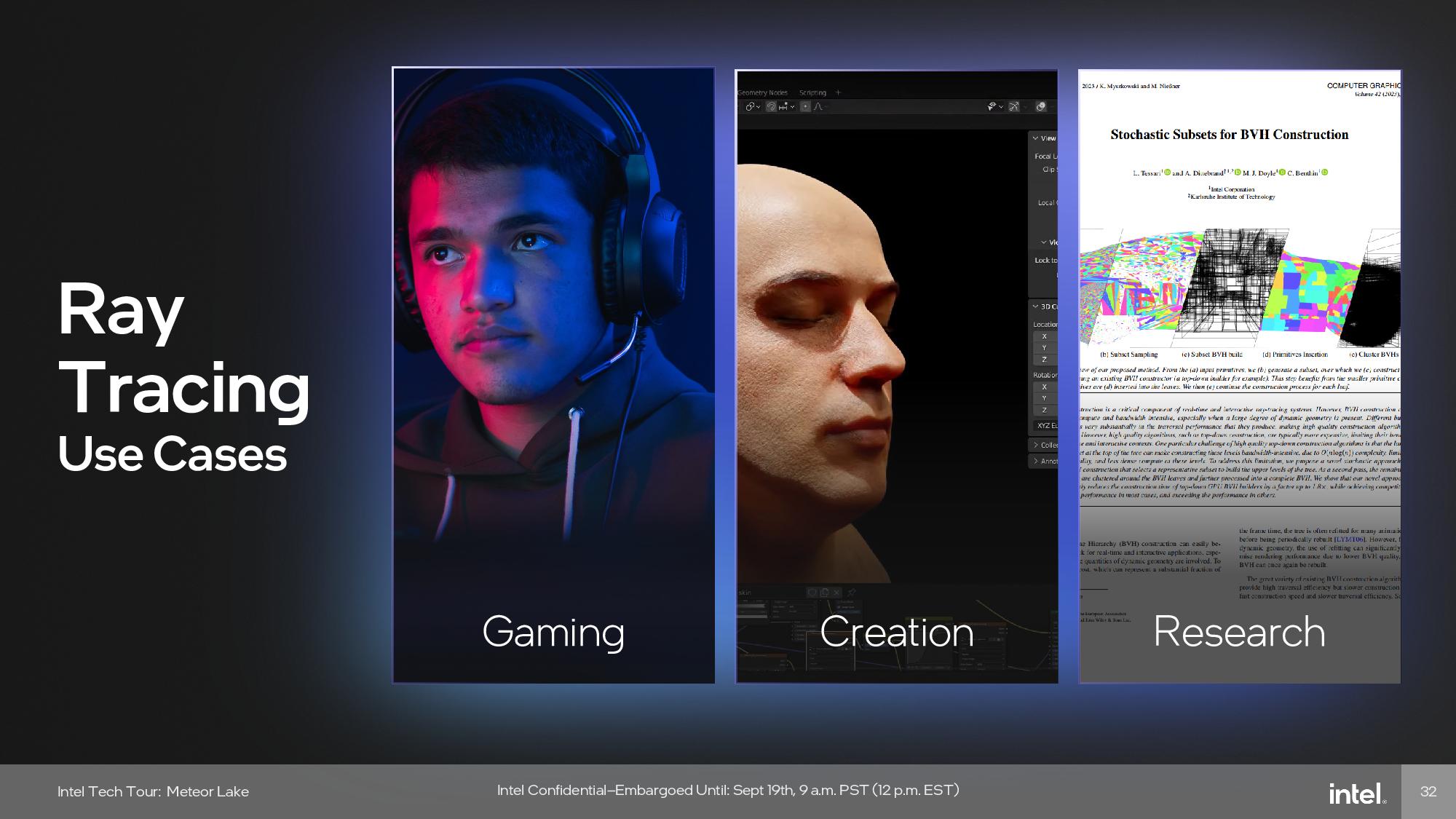
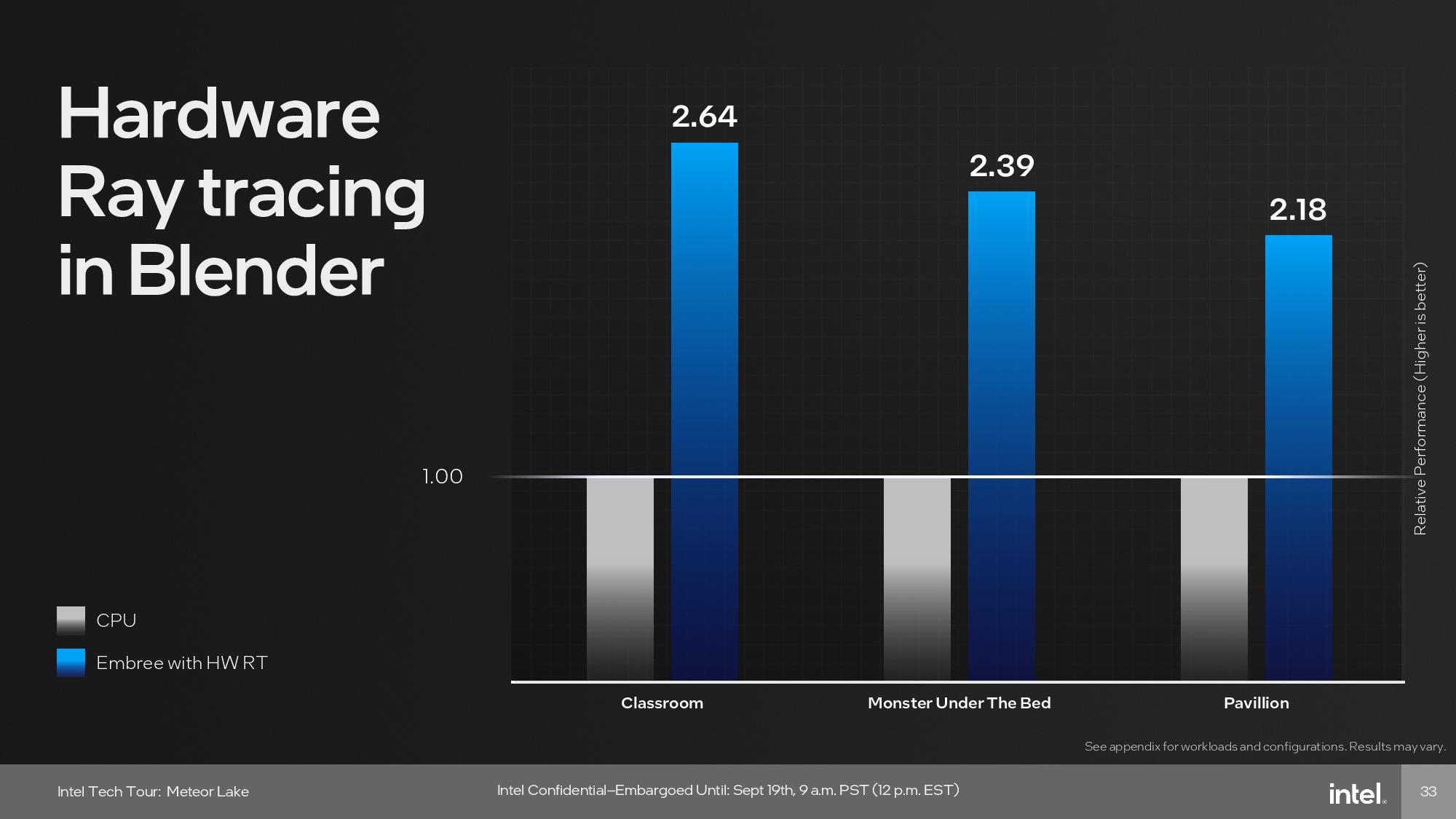
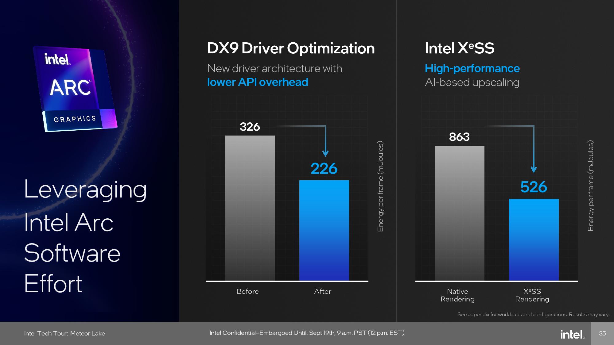
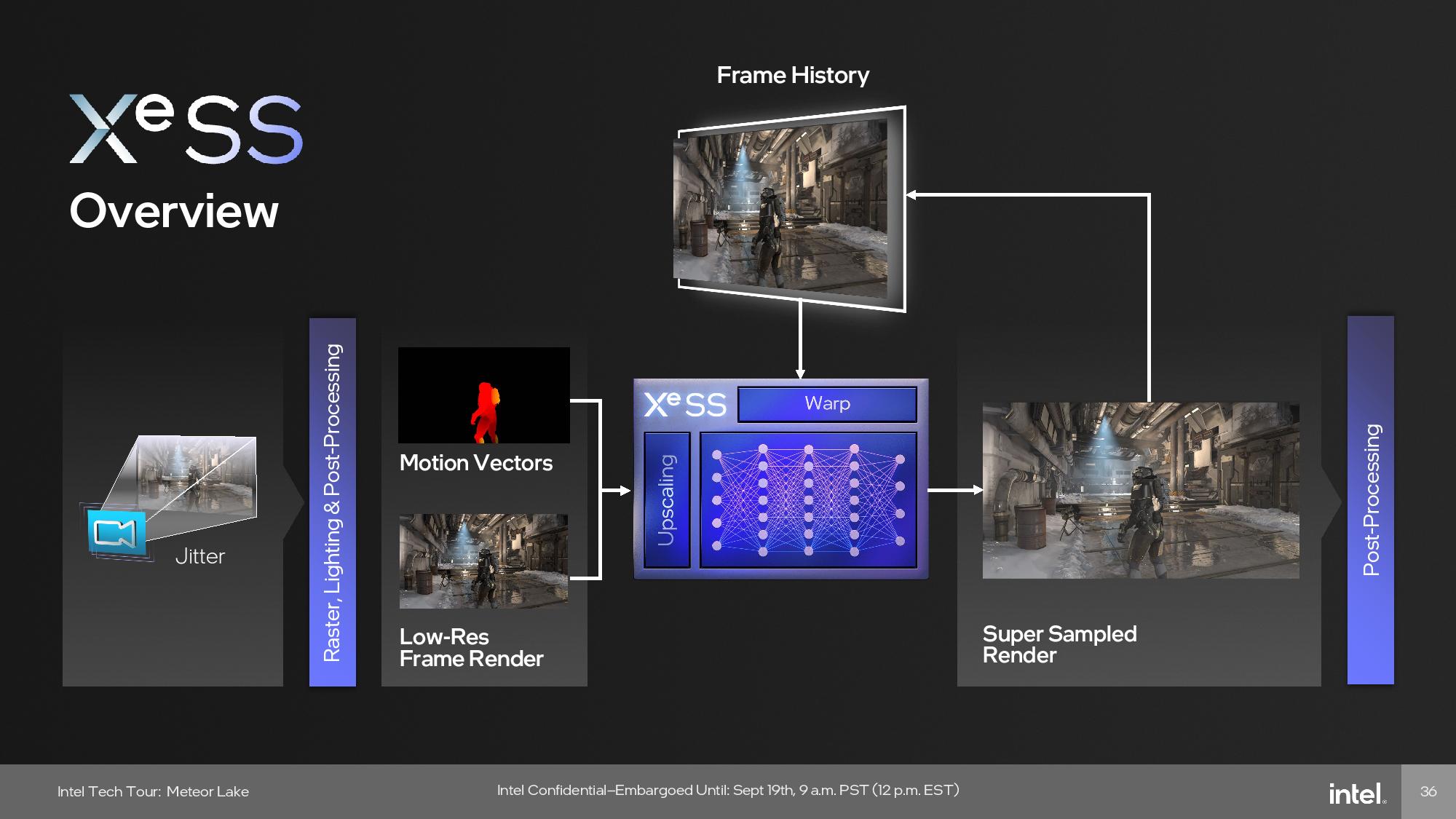
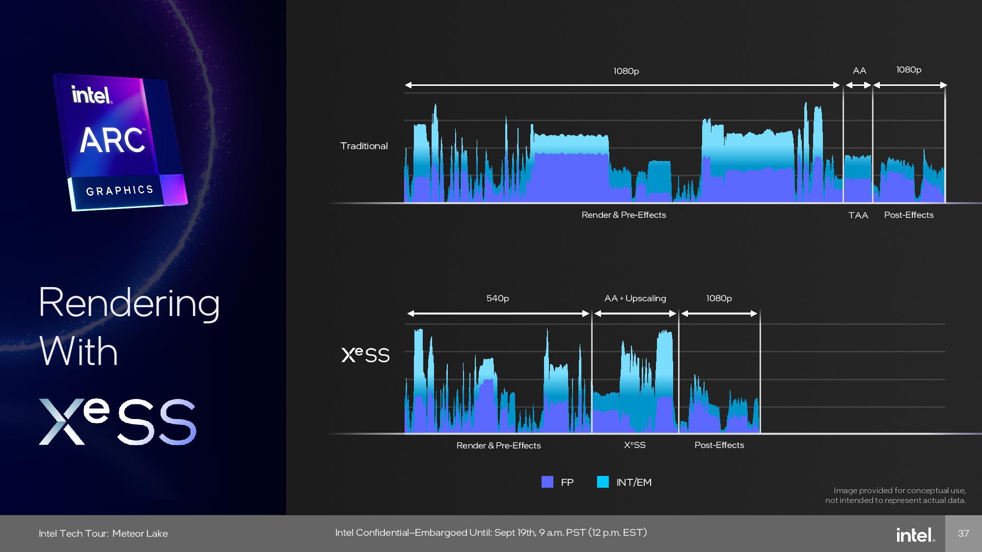
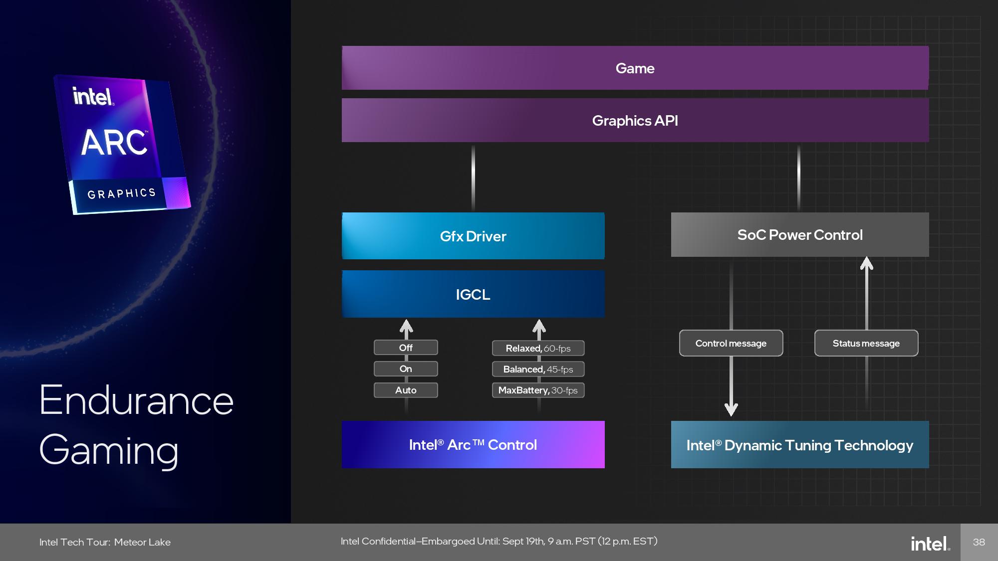
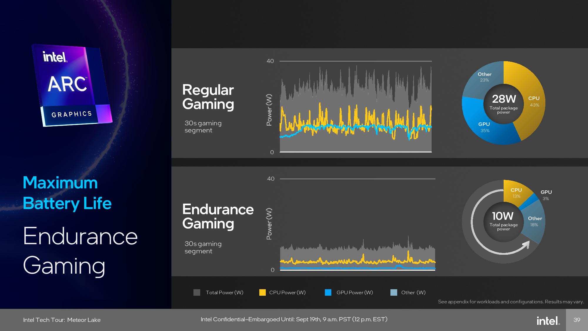
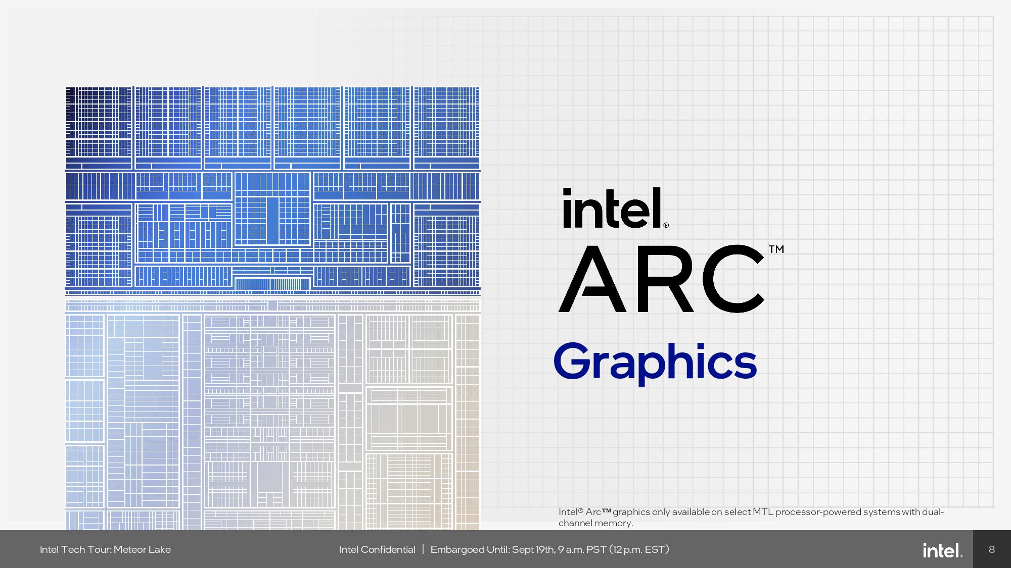
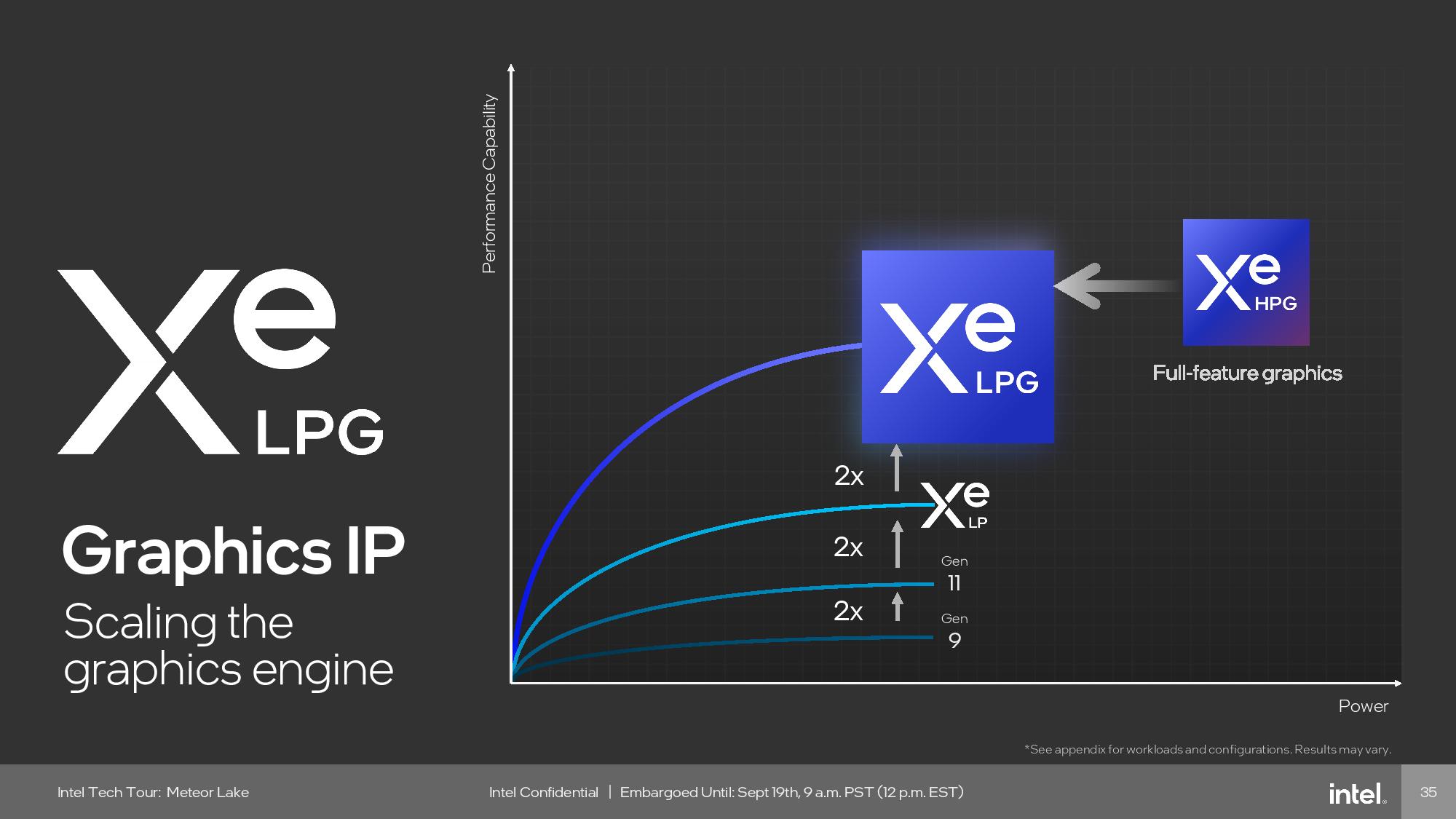
The GPU tile is fabbed on the TSMC N3 process node and employs Intel’s Xe-LP architecture, which now has many of the same features as Intel’s Xe-HPG architecture that’s found in its discrete graphics cards.
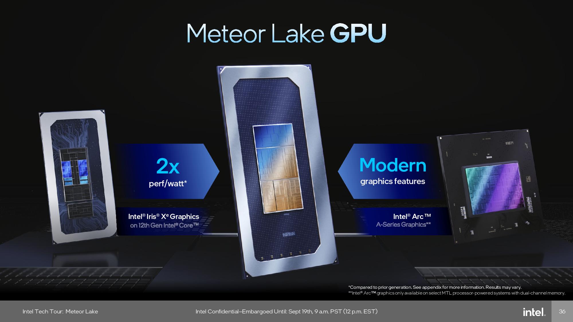
Intel claims a doubling of performance and performance-per-watt for this unit over the prior-gen, among other highlights. Intel also disaggregated the graphics tile by splitting off the Xe Media and Display engine blocks from the main engine on the GPU die and moving them onto the SOC tile, which helps with power consumption in many scenarios.
Naturally, the GPU tile is optimized for 3D performance, which includes hardware-accelerated ray tracing, mesh shading, variable rate shading, and sampler feedback. Intel also tuned the graphics engine’s voltage and frequency curve to run at much lower voltages and reach higher clock speeds. The GPU can also perform high-throughput AI operations using DP4A acceleration.
The slides above contain a good overview of the new design, and our resident GPU guru Jarred has written up a deeper dive on the Meteor Lake graphics unit, which you can read here.
Meteor Lake SoC Tile






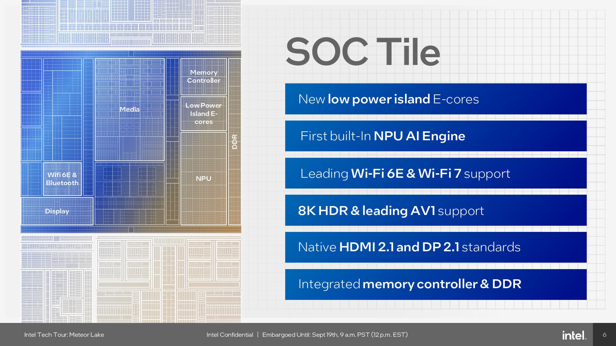
The SoC tile is fabbed on the low-power TSMC N6 process and serves as the central communication point for the tiles with a new-next gen uncore. Given the SoC tile’s focus on low power usage, Intel also calls it the low power island. The SoC tile comes with two new compute clusters, the two low-power-island e-cores and Intel’s Neural Processing Unit (NPU), a block that’s used entirely for AI workloads, among many other units.
Intel moved all the media, display and imaging blocks from the GPU engine to the SoC tile, which helps maximize power efficiency by allowing those functions to operate on the SoC tile while the GPU is in a lower power state. The GPU tile is also fabbed on the more expensive TSMC N5 node, so removing these non-performance-sensitive blocks allowed Intel to better utilize the pricier transistors on the GPU tile for graphics compute. As such, the SoC tile houses the display interfaces, like HDMI 2.1, DisplayPort 2.1, and DSC 1.2a, while also supporting 8K HDR and AV1 encoding/decoding.
The SoC tile resides next to the GPU tile, and the two communicate over a die-to-die (tile-to-tile) interface on one side of the die. You can see this tile-to-tile interface in the above album. Each side of the interconnect has a primary mainband interface that provides the bandwidth required to pass data between the chips. This connection runs through the underlying Foveros 3D silicon, thus providing a much more efficient pathway than standard traces that run through organic substrates (like PCBs). Additionally, a secondary connection provides the interfaces for clock, test and debug signals, along with a dedicated Power Management Controller (PMC) interface between the tiles.
The GPU is connected to an isolated high-performance cache-coherent network on chip (NOC) that connects the NPU, low-power e-cores, and media and display engines to ensure they have efficient access to the memory bandwidth provided by the memory controllers that also reside on the same bus. This NOC also connects to the compute (CPU) tile via another tile-to-tile interface on the other side of the tile.
Intel has a second lower-power IO Fabric (not coherent) that connects to the I/O tile via another tile-to-tile interface. This IO fabric also contains other lower-priority devices, like Wi-Fi 6E and 7, Bluetooth, the security engines, ethernet, PCIe, SATA, and the like.
That leaves Intel with two independent fabrics on the die, but they must be able to communicate with one another. Intel connected the two with an I/O Cache (IOC) that buffers traffic between the two fabrics. This does incur a latency penalty for cross-fabric communication between the two buses, but the additional latency falls within performance targets for the low-priority I/O fabric.
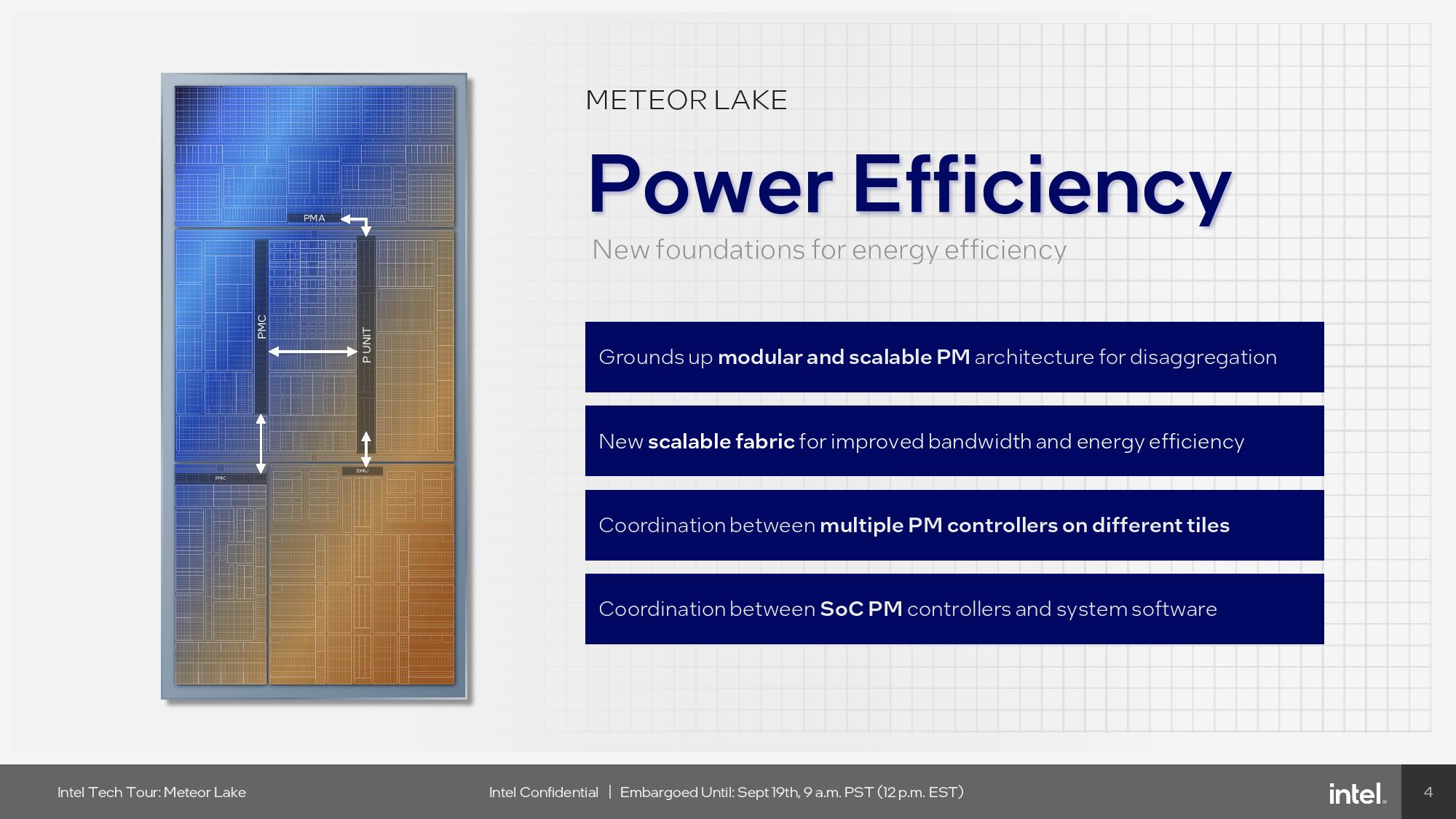
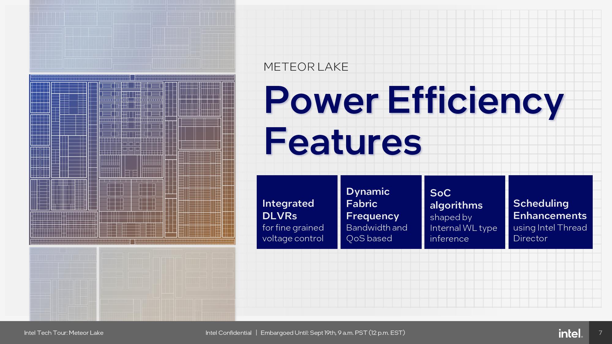
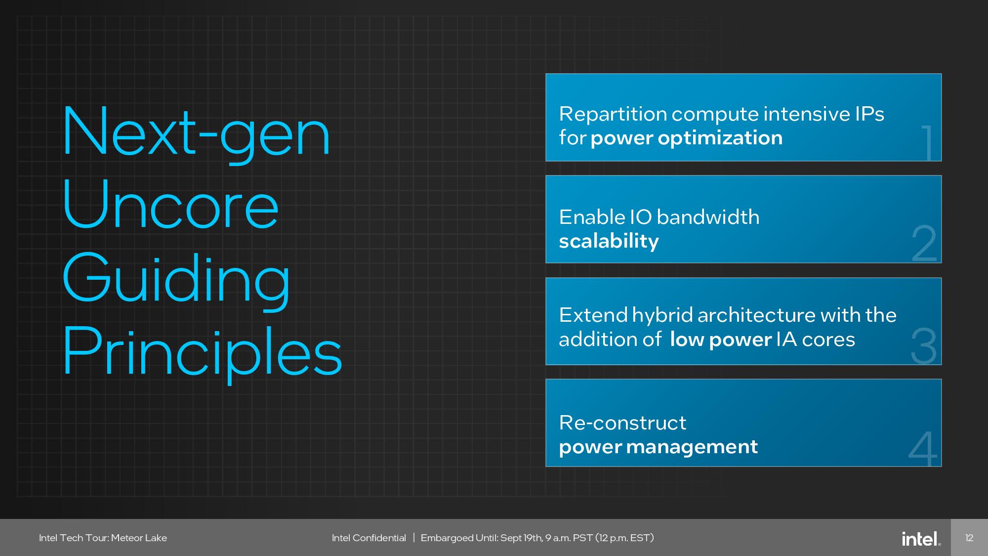
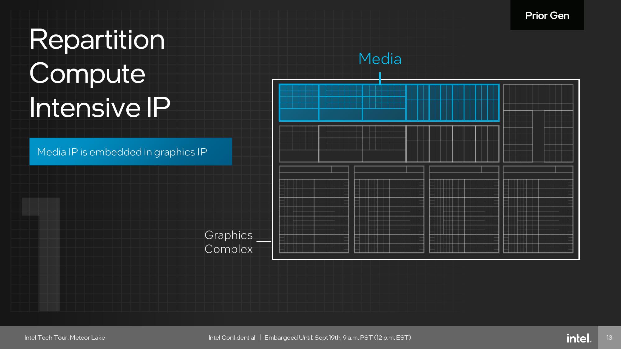
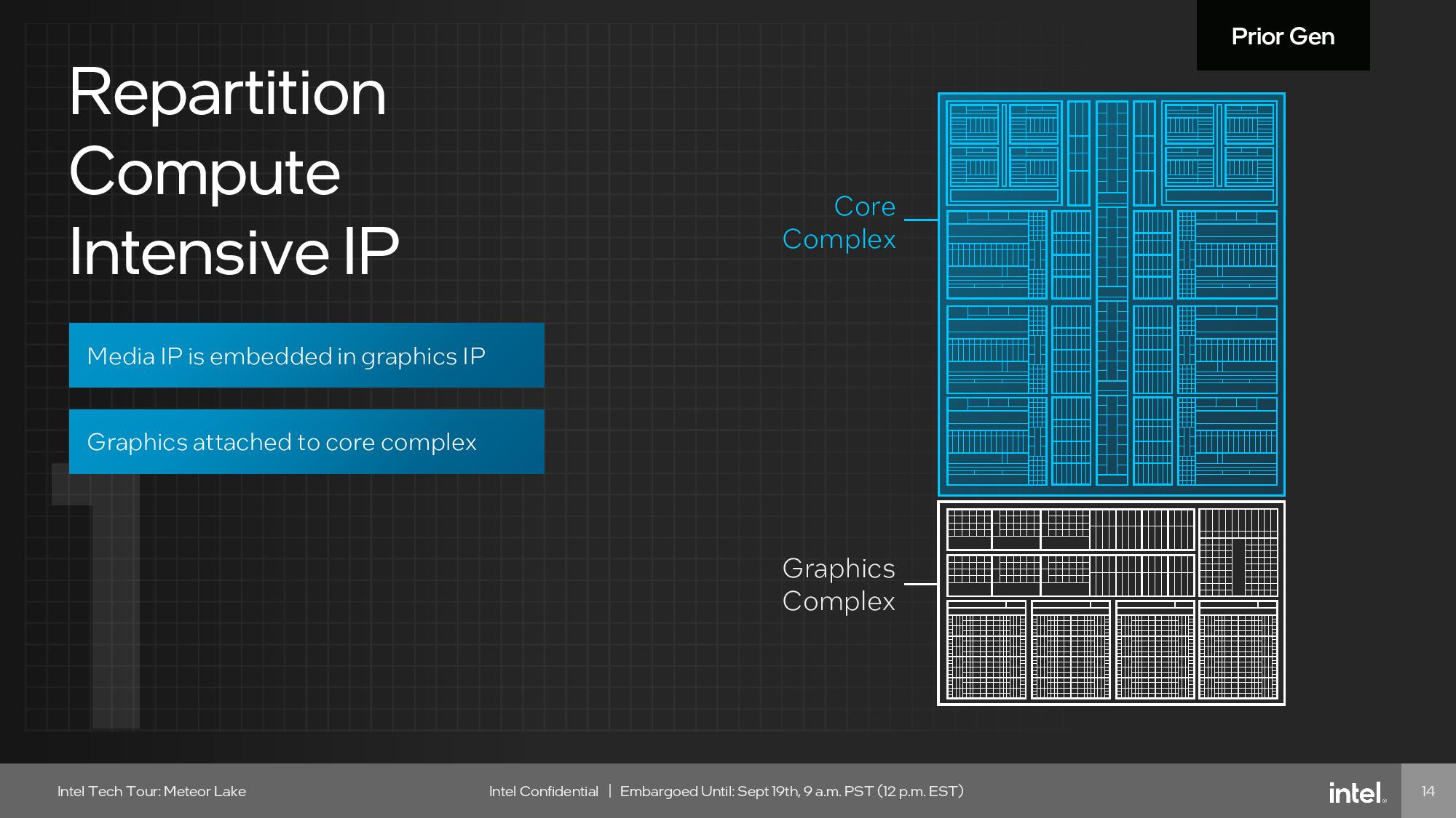
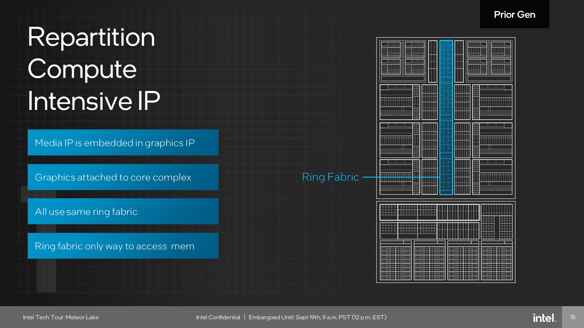
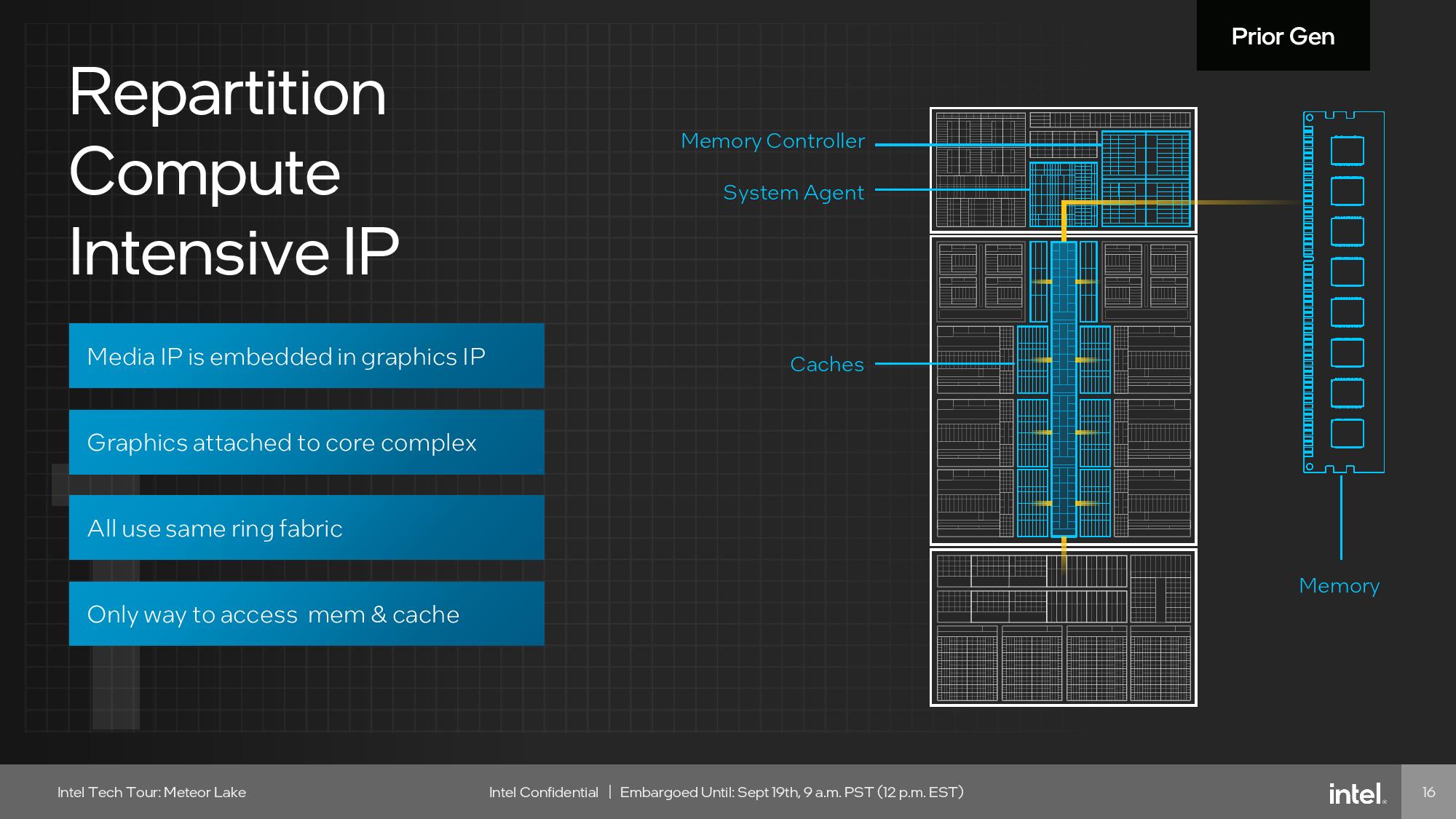
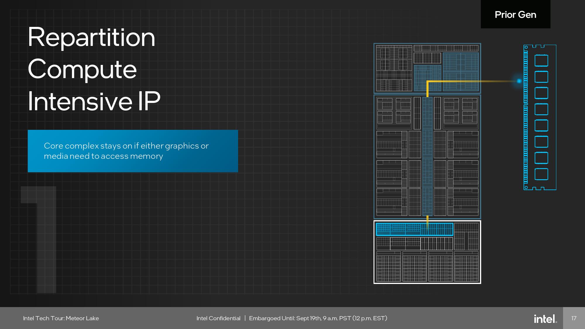
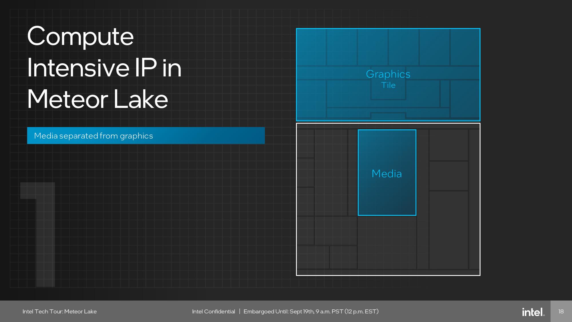
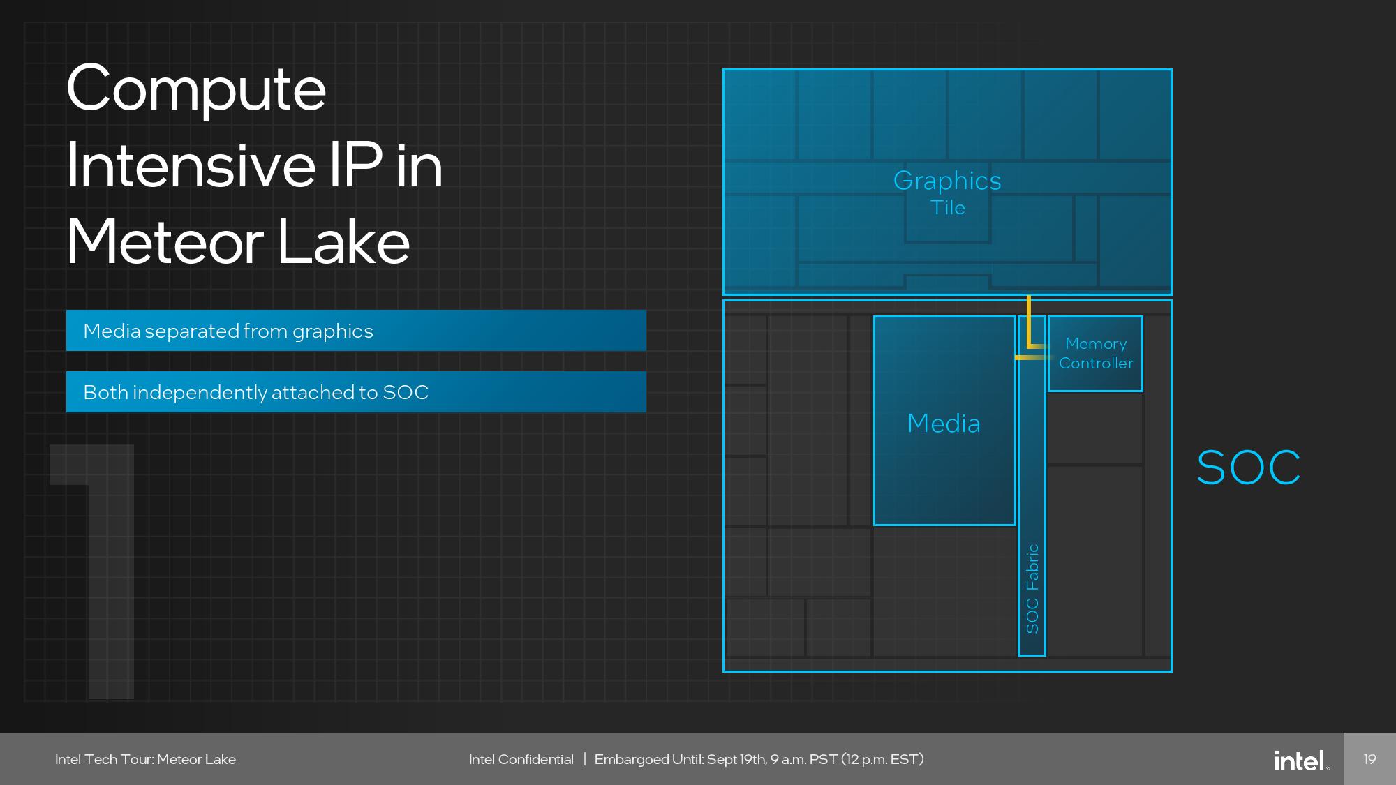
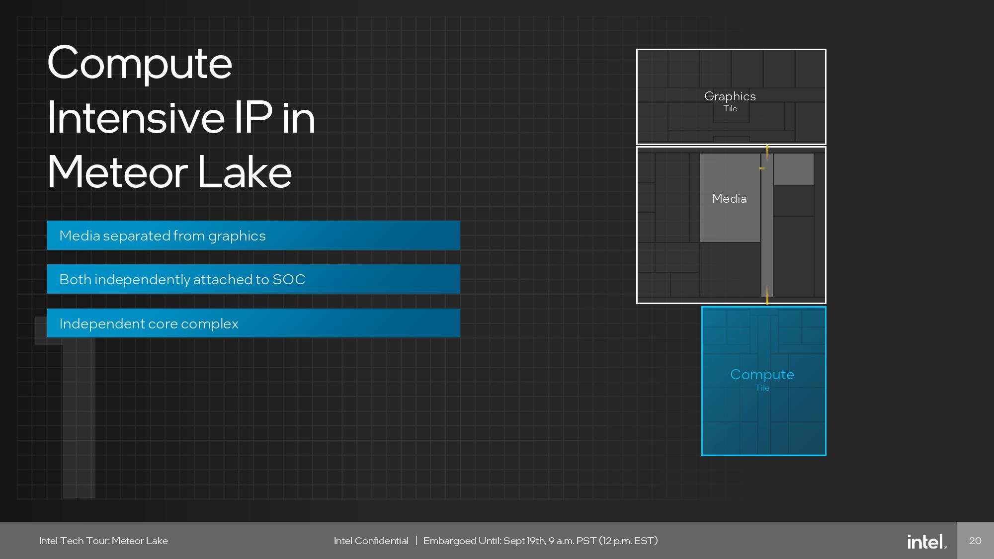
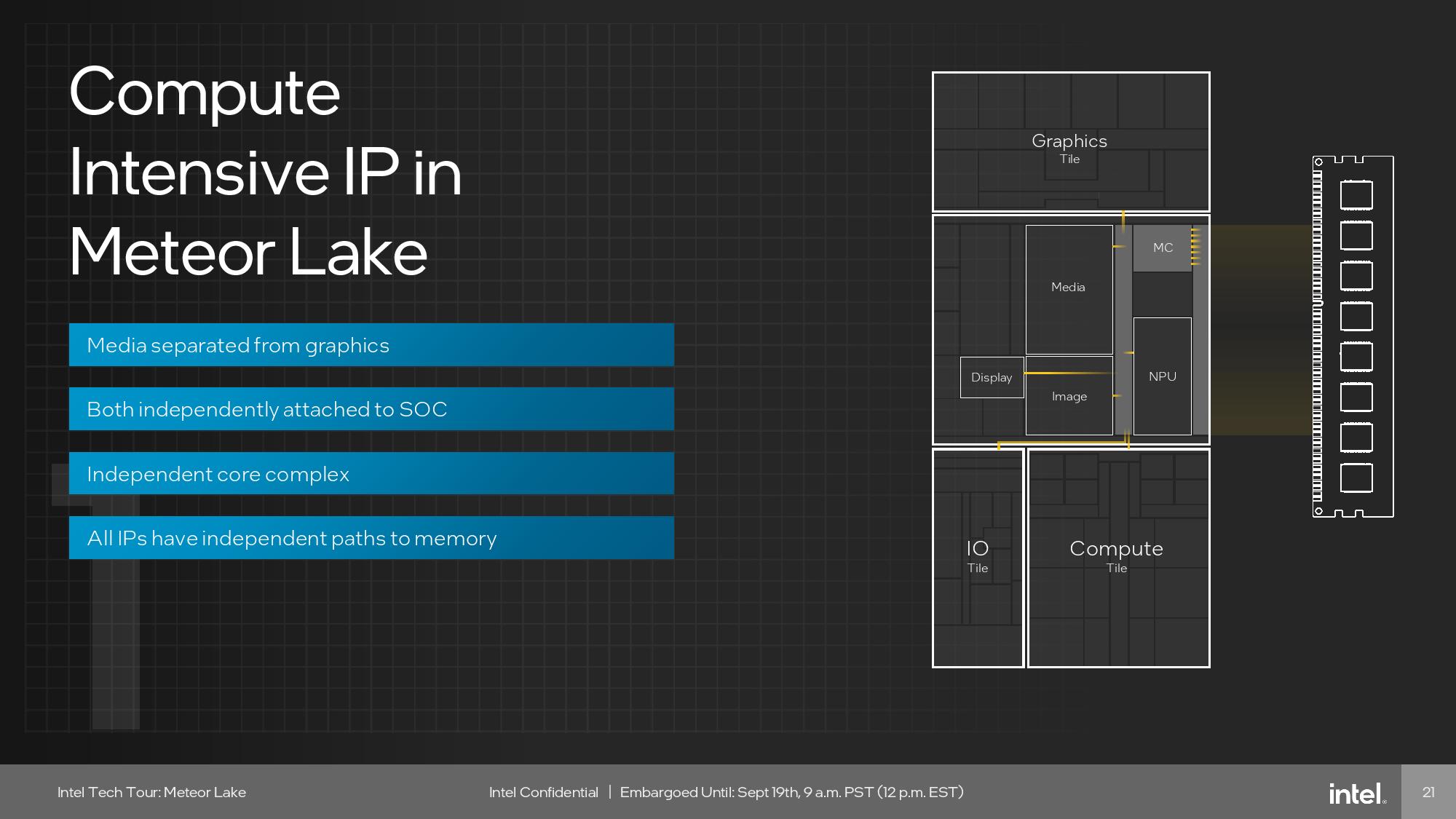
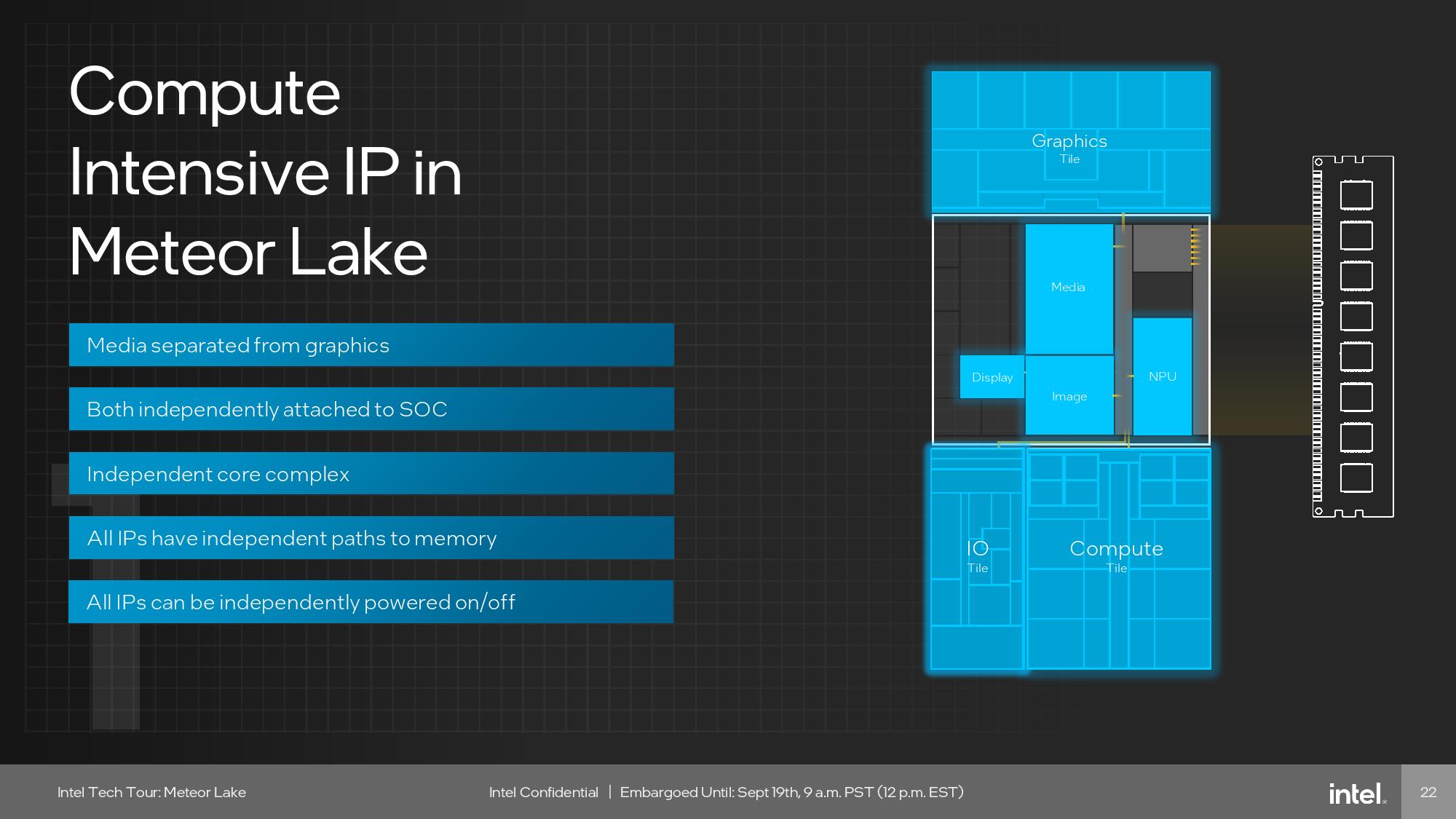
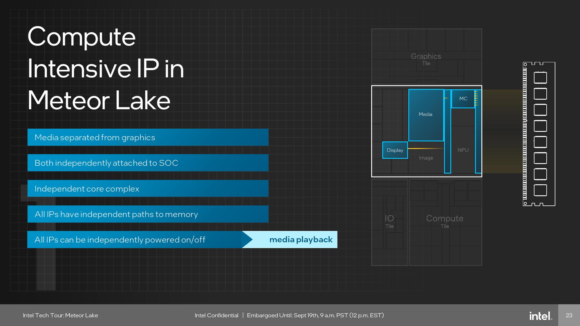
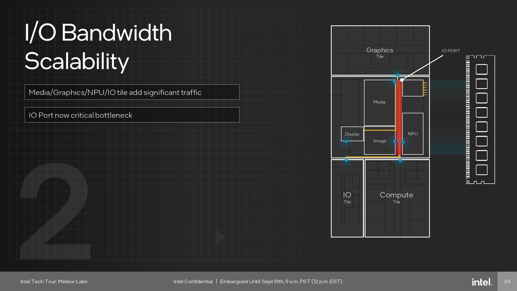
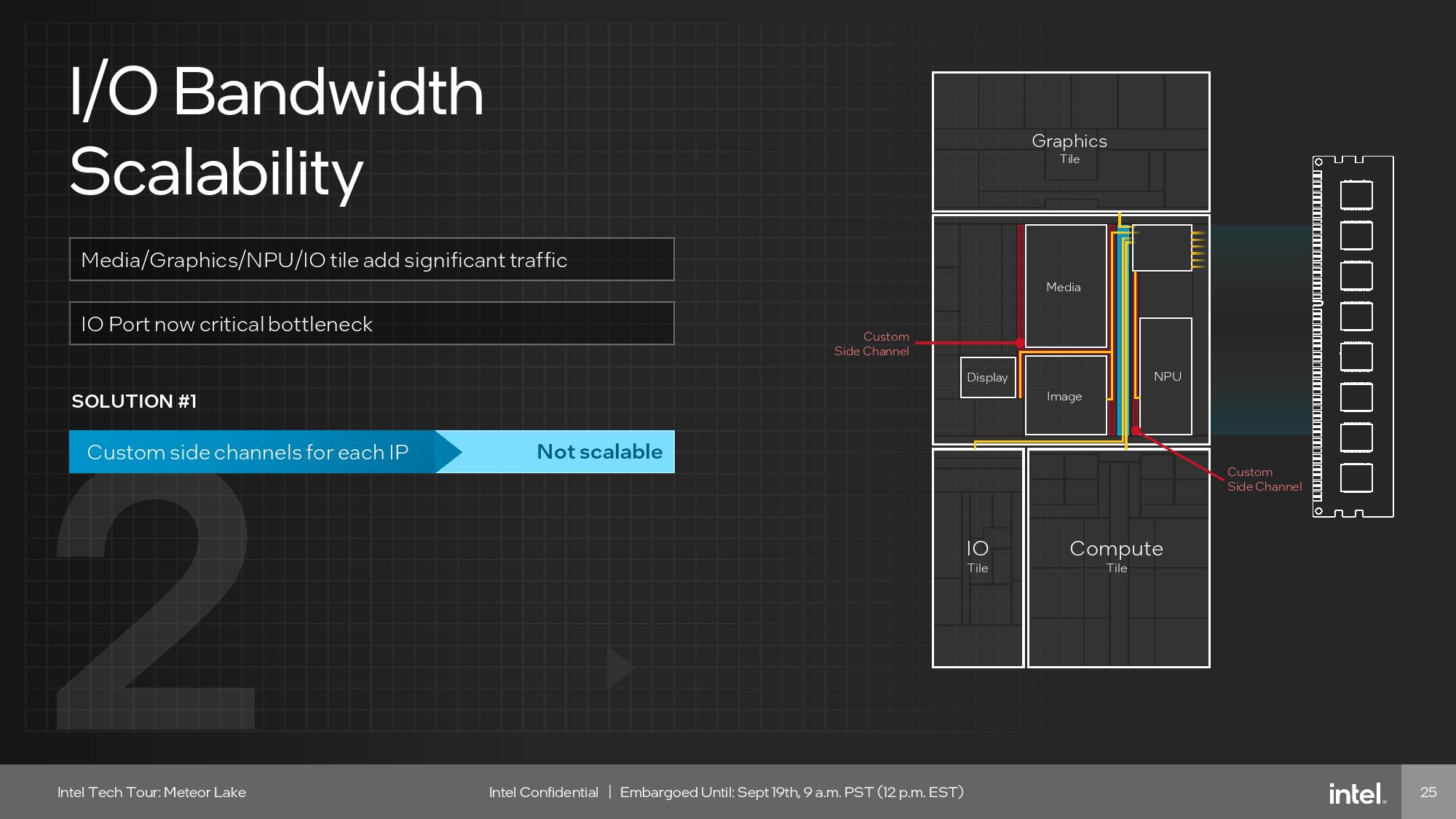
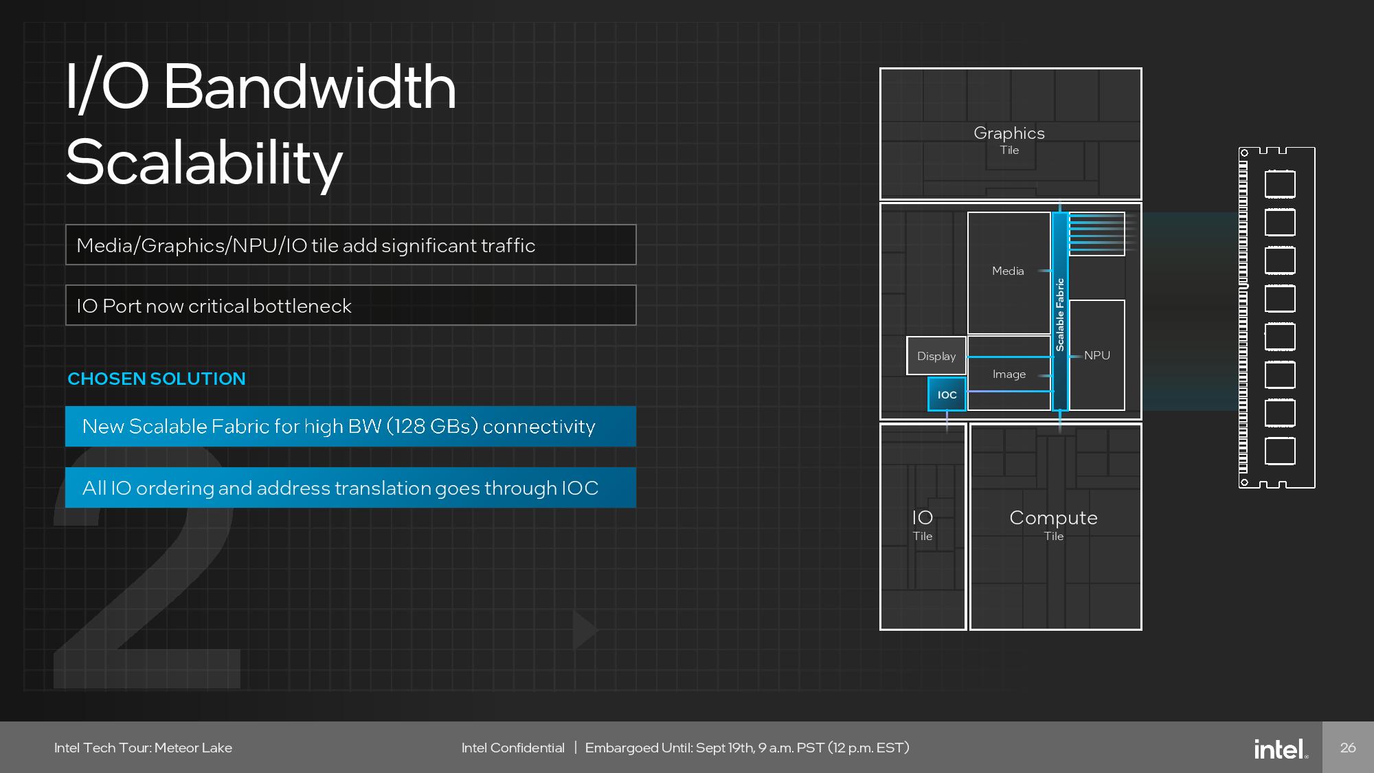
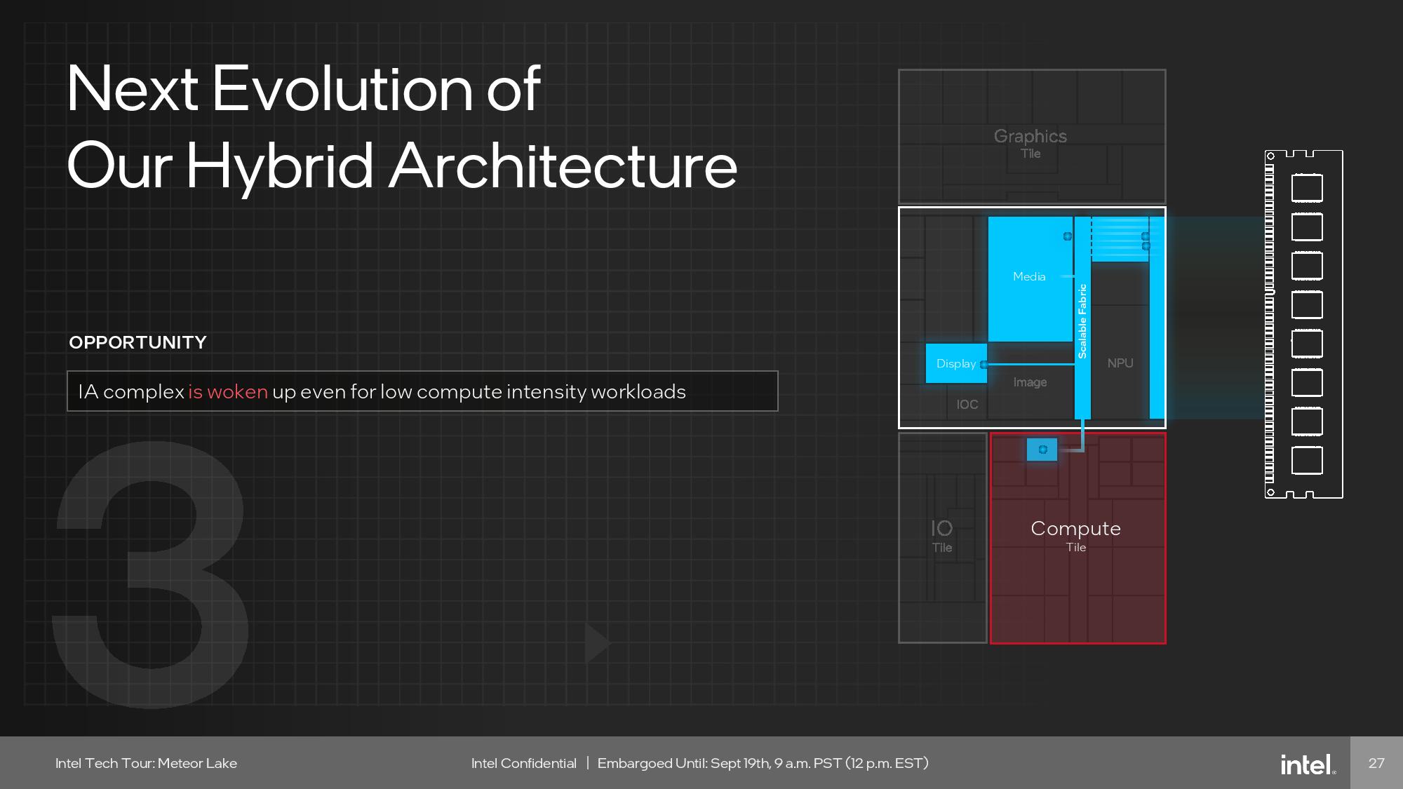
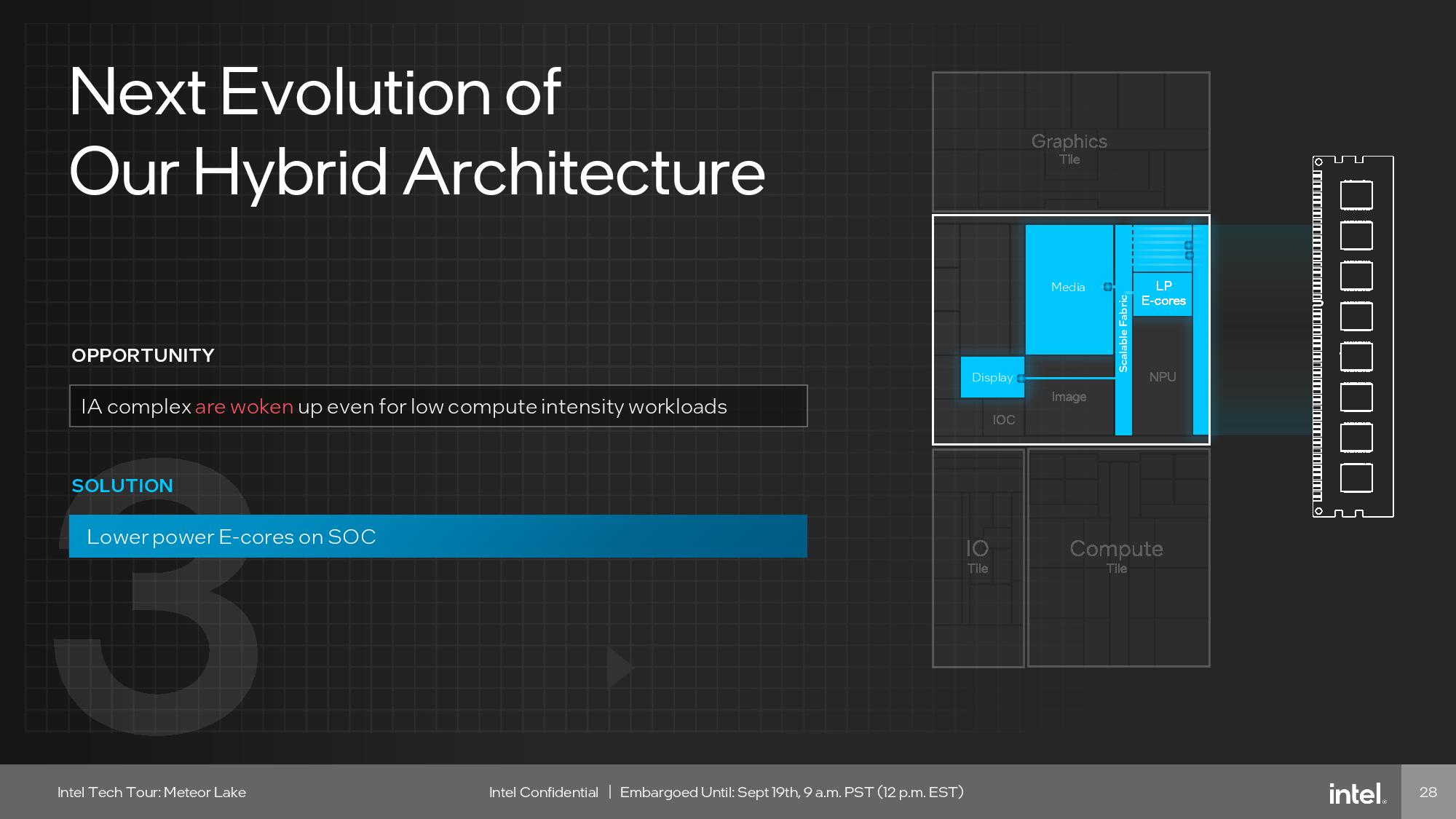
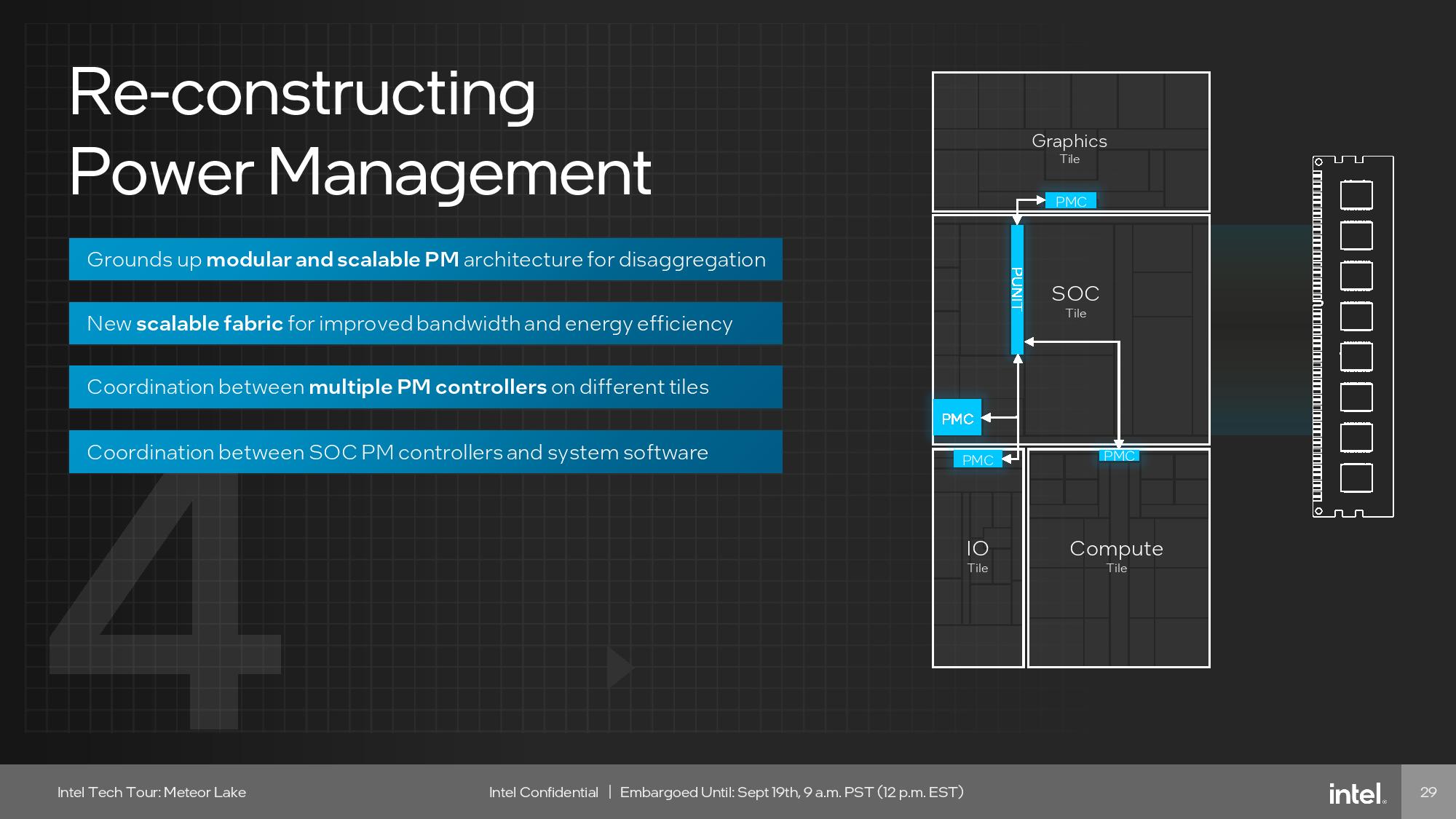
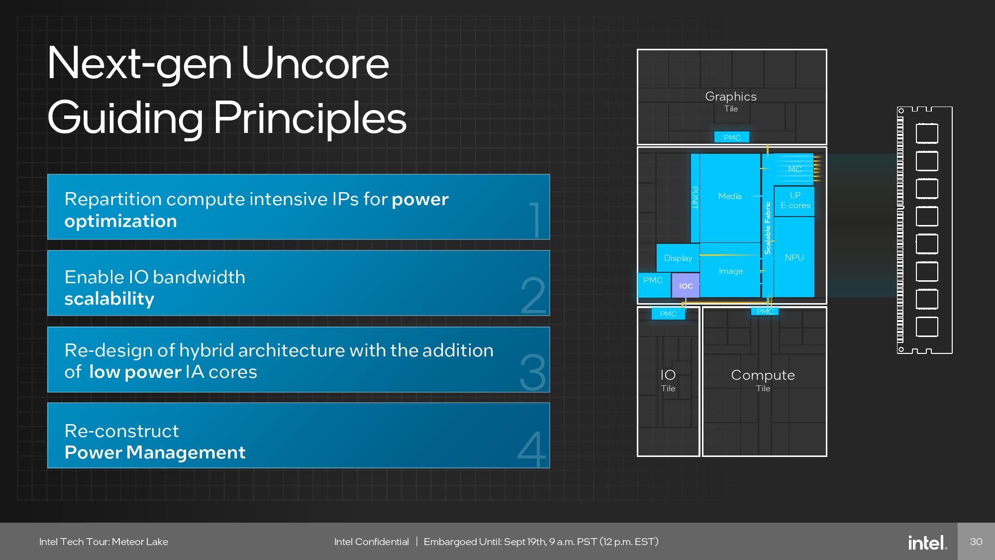
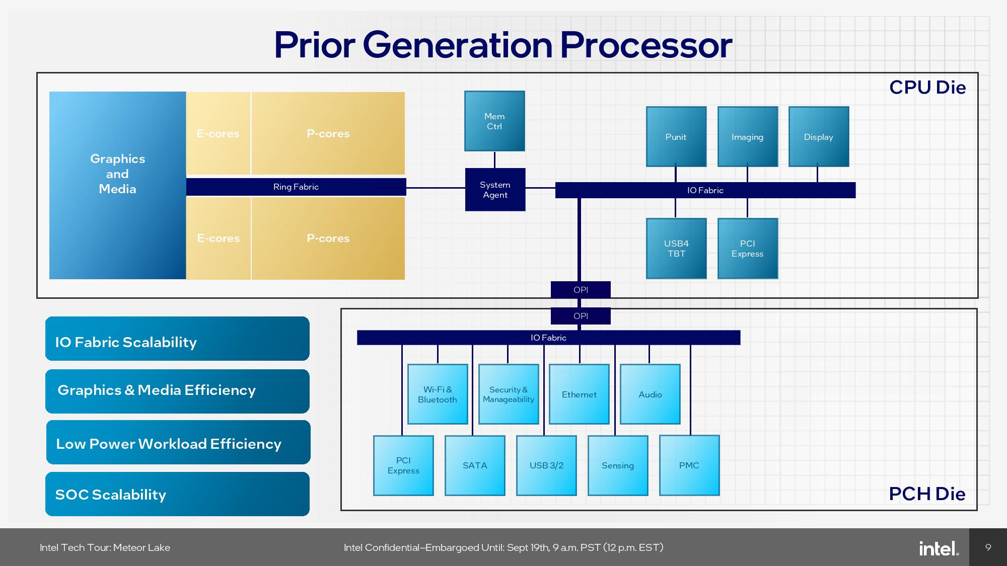
Intel refers to this new fabric hierarchy as the next-generation Uncore. As you can see in the image album above, the previous-gen chip design placed the devices on an I/O fabric that communicated through a system agent controller connected to isolated memory controllers. However, this system agent also controlled memory bandwidth flowing to the ring fabric that connects the CPU cores, thus creating unnecessary contention and bandwidth constraints. That simply wasn’t scalable enough to handle the addition of more bandwidth-hungry devices, like the NPU and low-power E-cores, to the I/O fabric.
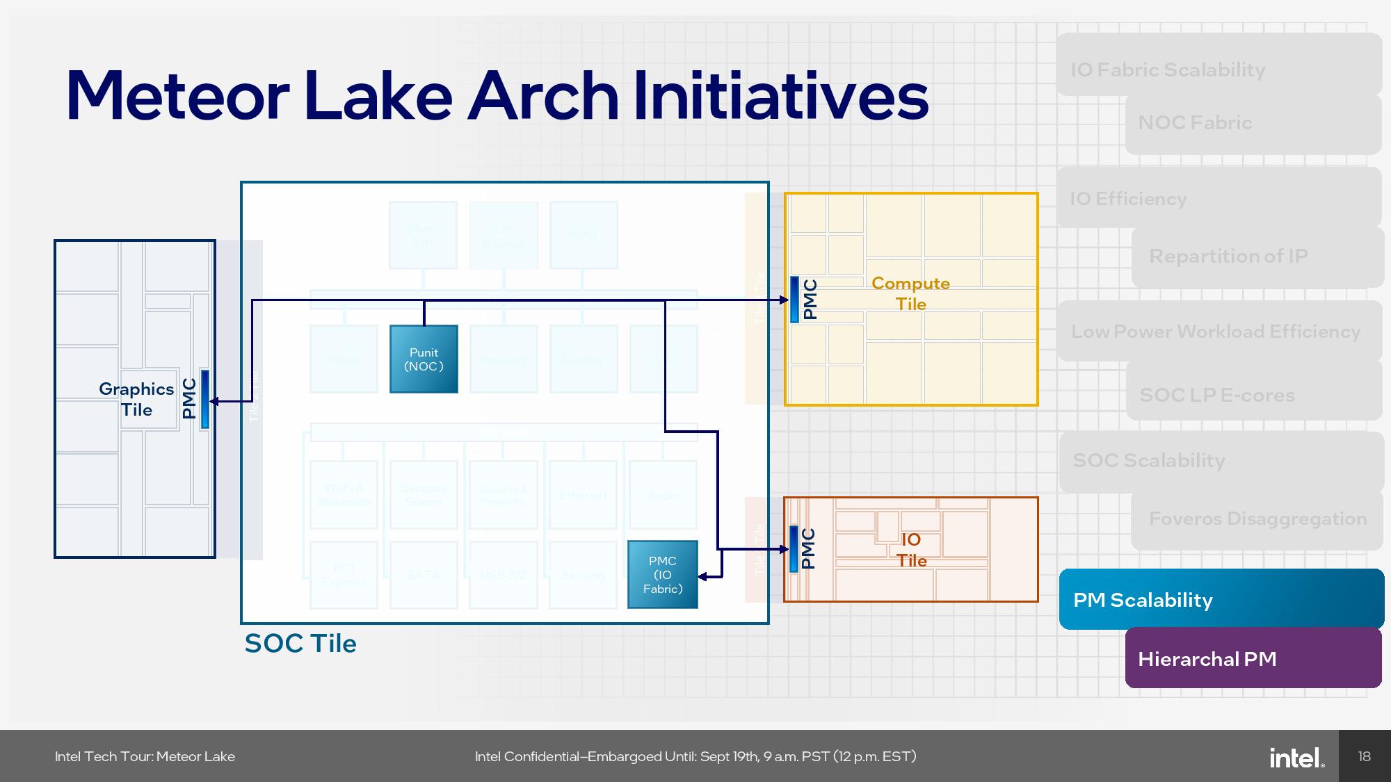
The next-gen uncore solves those issues, and more, as you can see when you step through the slides. Intel has also now added an independent power management controller (PMC) to each tile for independently voltage and frequency control. However, those are all connected to two PMCs on the SoC tile that control the independent fabrics, thus creating a power management hierarchy that affords greater energy savings. All tiles also contain their own DLVRs to closely modulate voltages, along with dynamic fabric frequencies that adjust based on bandwidth and quality of service requirements.
Meteor Lake I/O Tile
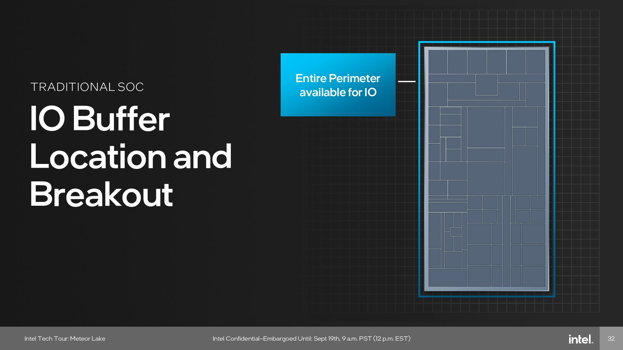
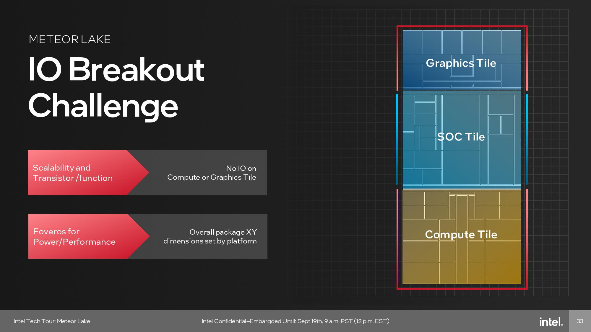
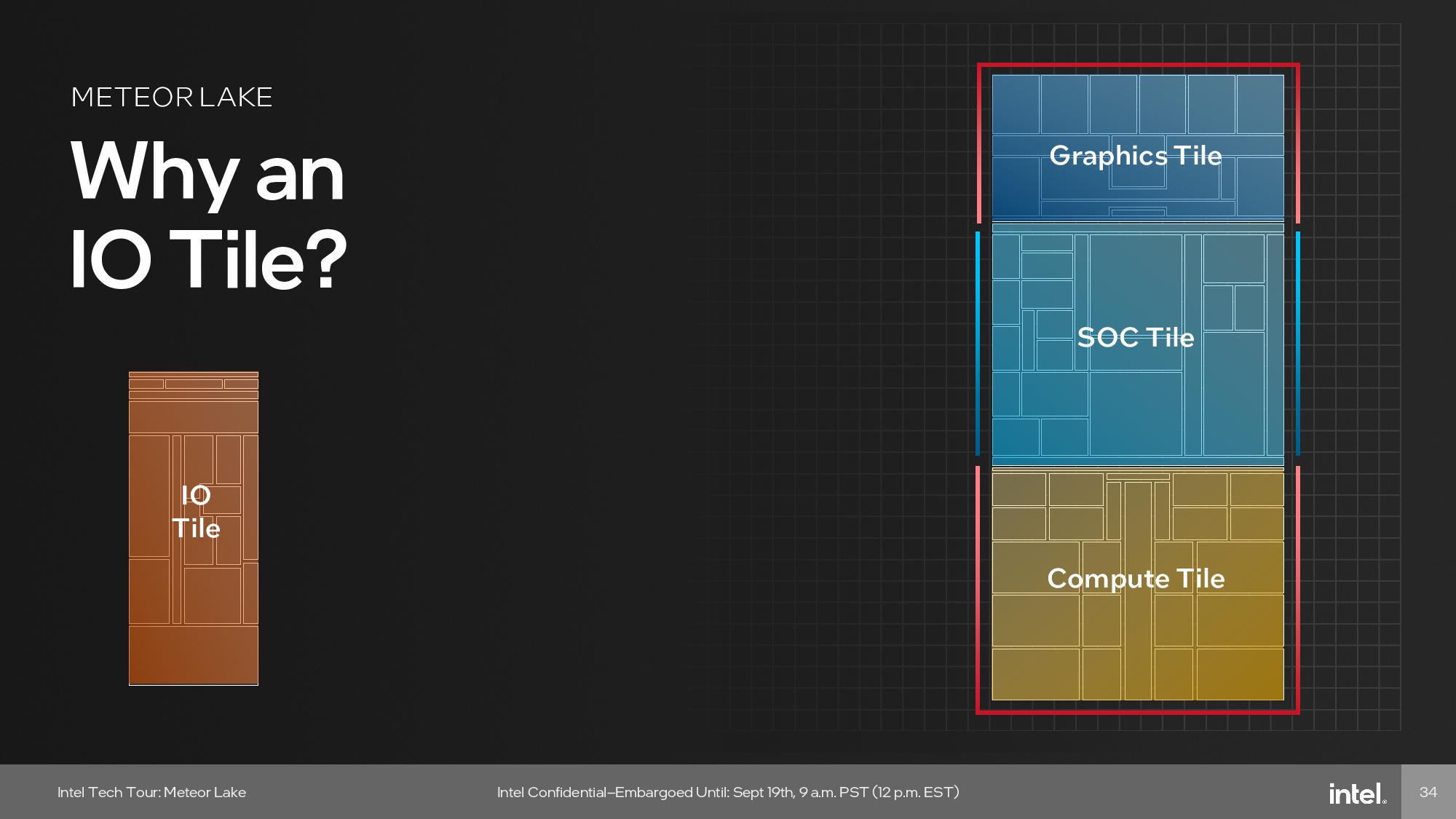
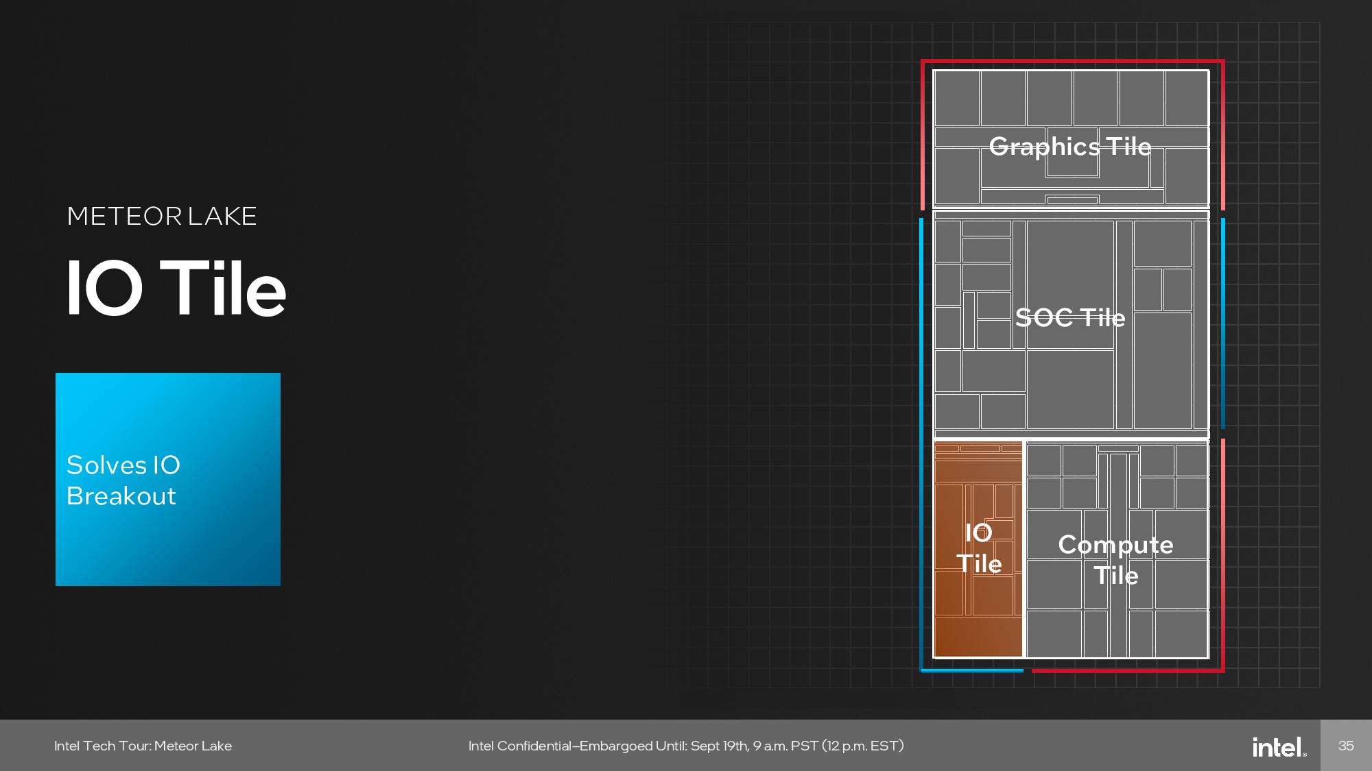
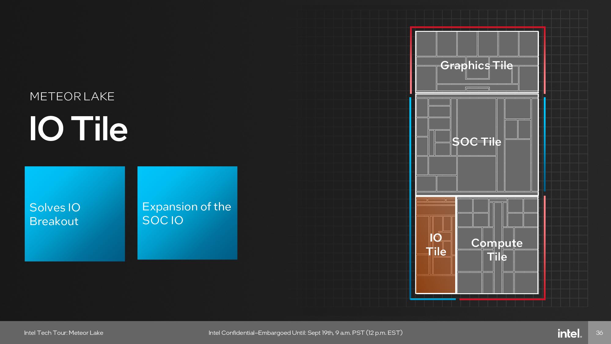
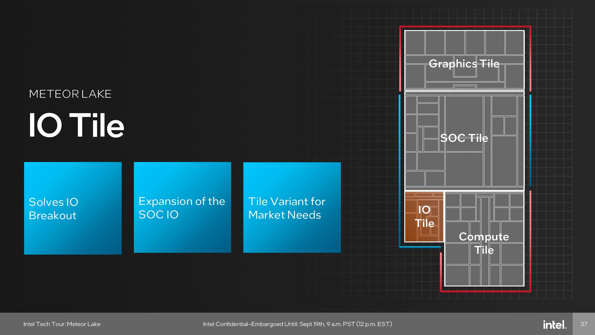
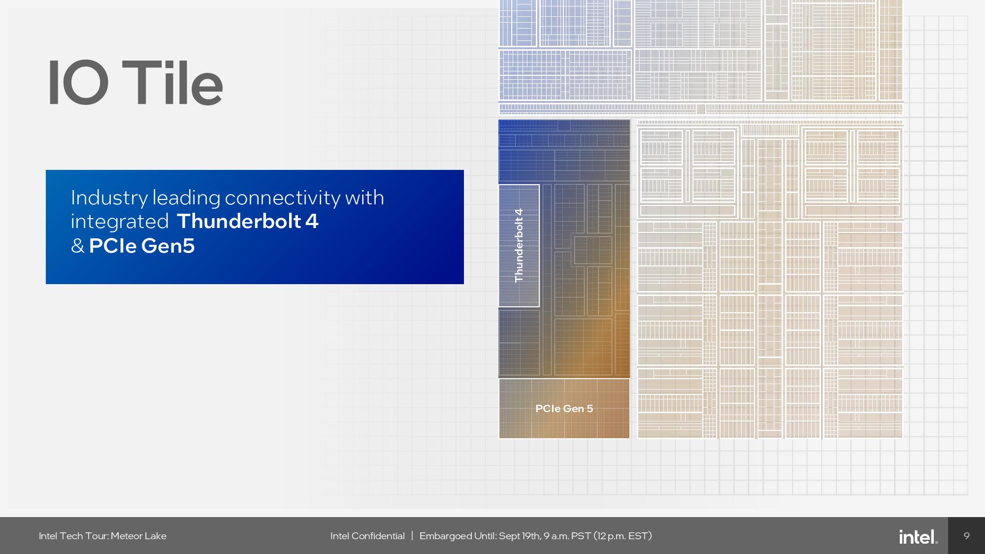
Intel’s next-gen uncore design methodology isn’t without drawbacks, though. The SoC tile houses the DDR5 memory and PCIe controllers, but those external interfaces can only be placed on two sides of the die – the other two sides are used for communication with the other tiles. This presents a limitation on the number of connections that can be placed on those edges of the die (shoreline). To solve this problem, Intel created a secondary I/O tile to enable more room for connections to additional PCIe lanes and the Thunderbolt 4 external interface. Other options, like changing the aspect ratio of the SoC tile, won’t work due to compatibility issues with existing socket interfaces.
The I/O tile is the smallest of the four Meteor Lake tiles and is fabbed on the TSMC N6 process. This tile houses I/O functions like Thunderbolt 4 (yes, not version 5) and PCIe Gen 5.0. Intel will use different sizes of I/O tiles for different products based upon the amount of connectivity required.
Low Power Island E-Cores
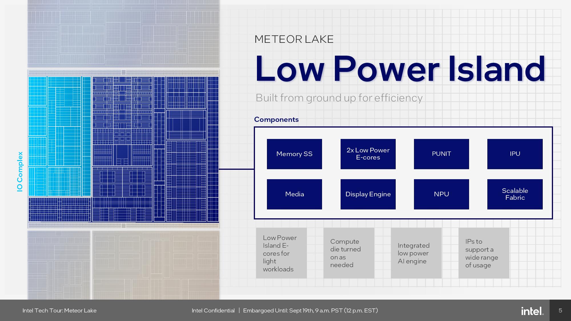
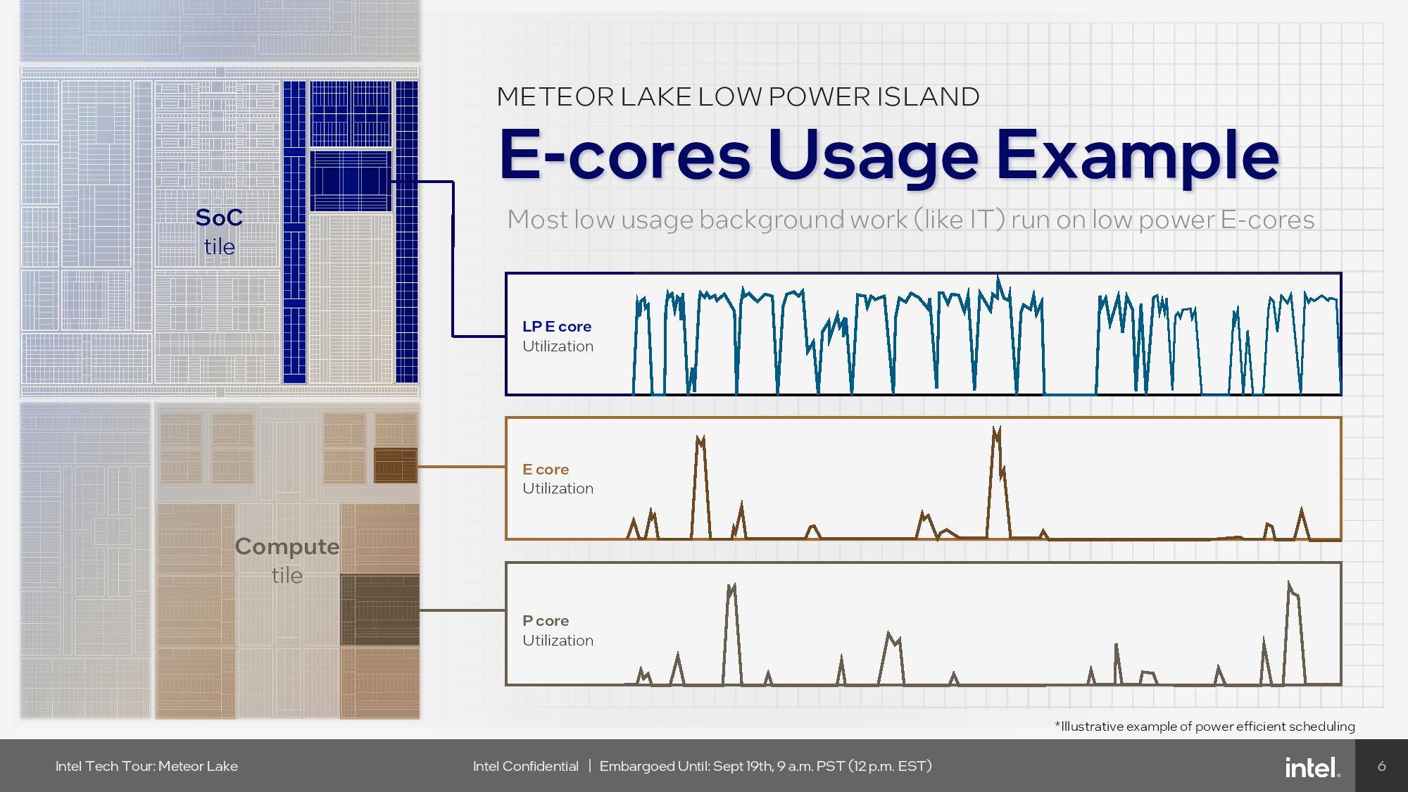
Intel’s SoC tile comes with two low-power E-cores that use the same Crestmont microarchitecture we described in the compute tile section. These low-power cores can run the operating system in certain light usage modes, like while playing back video, allowing the entire compute tile to be placed into a low power mode to conserve energy. Additionally, the cores can handle many of the day-to-day light background tasks that don’t require the heft of the quad-core E-core clusters on the compute tile, thus allowing it to put individual cores to sleep more often. Intel hasn’t shared specifics about the performance of these cores, but we do know they are tuned specifically for TSMC’s low-power N6 node.
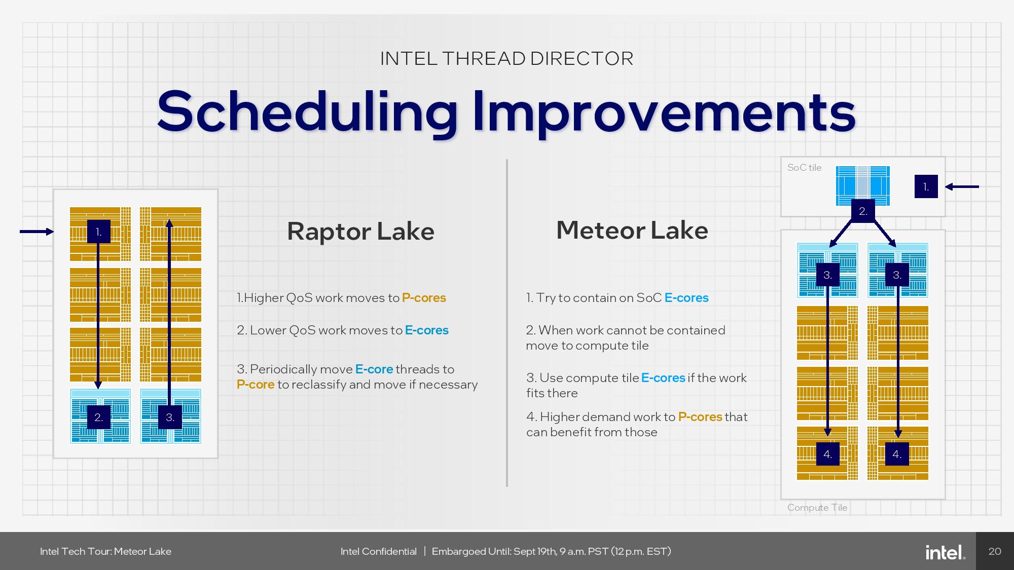
Intel also indicated that Thread Director will now prioritize the low-power E-cores first when it decides where to place any given thread that isn’t specifically targeted at a certain core type. However, if a thread begins to run on the low-power e-cores and it becomes evident it needs more compute power, the operating system will move it to a faster core. In the past, Thread Director prioritized the P-cores as the first-order destination for any given workload. The decision to prioritize these low power e-cores raises questions about the impact on performance responsiveness, but we won’t know the full impact until chips land in our labs.
Neural Processing Unit (NPU)
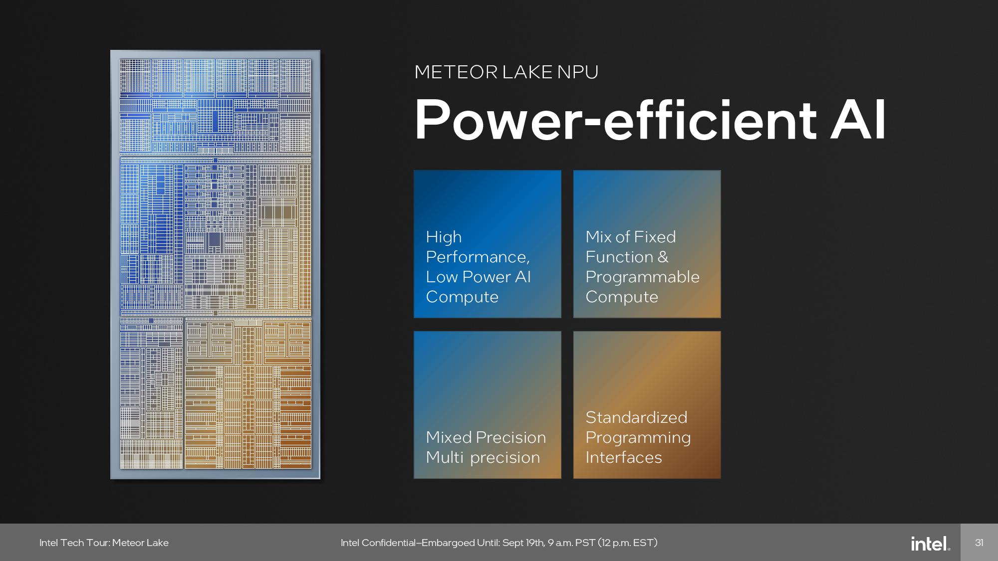
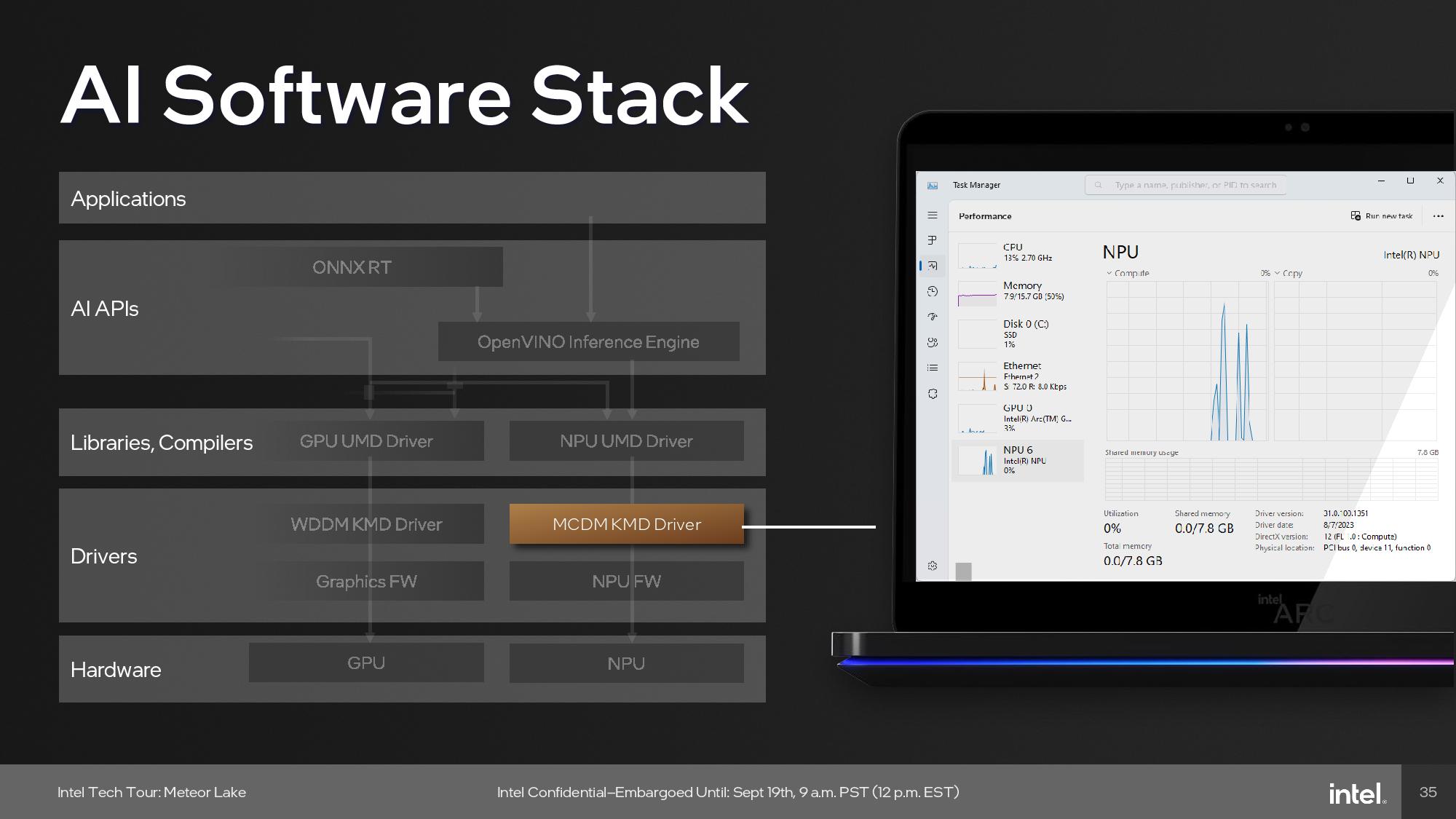
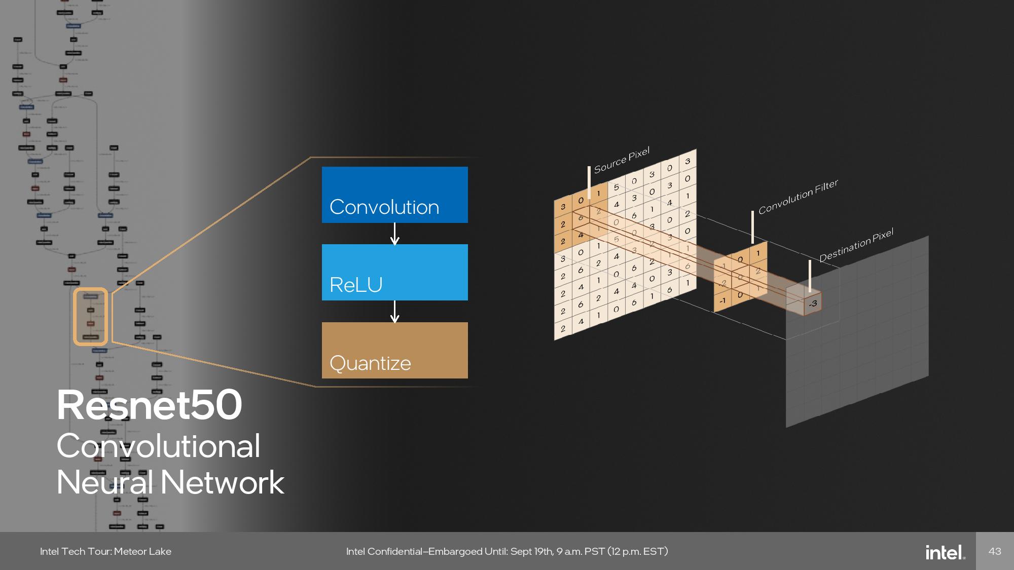
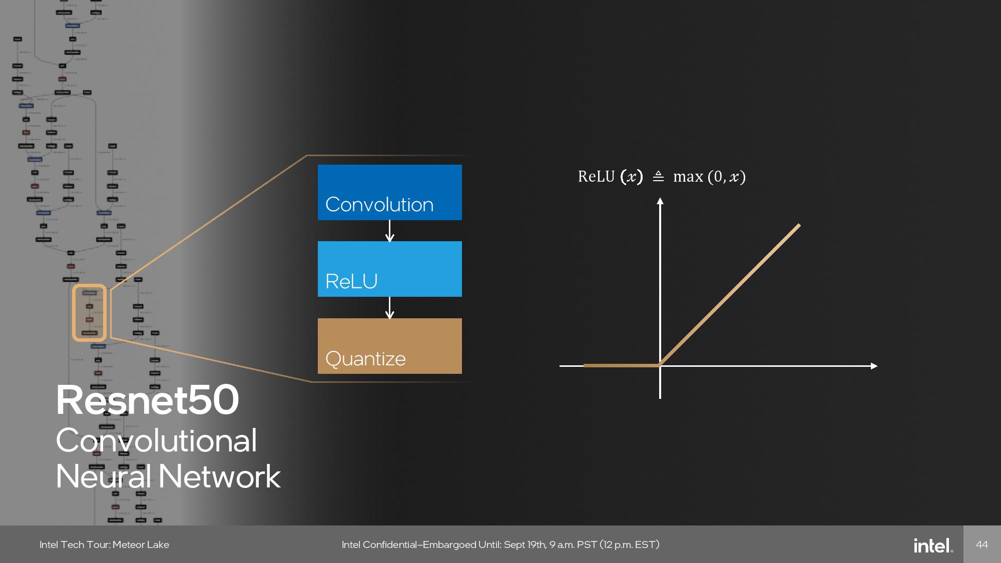
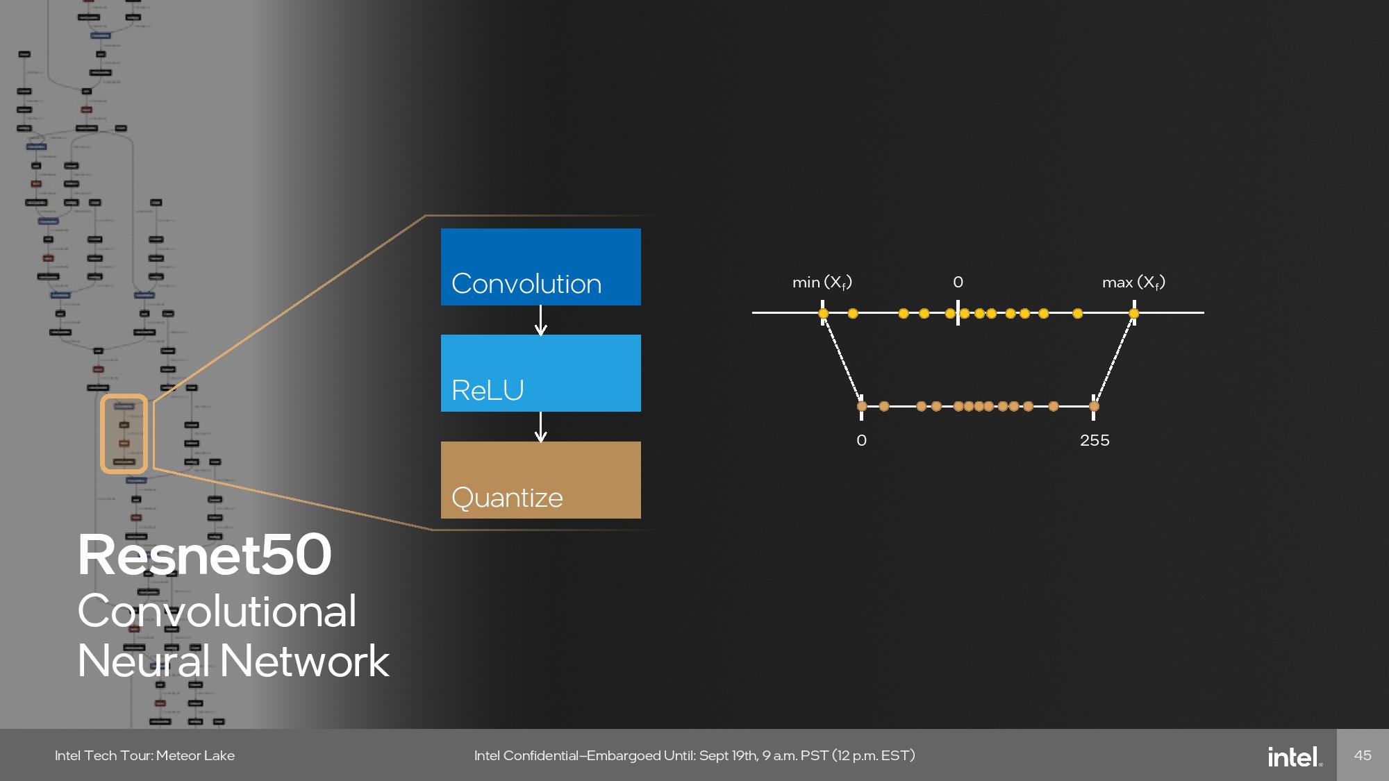

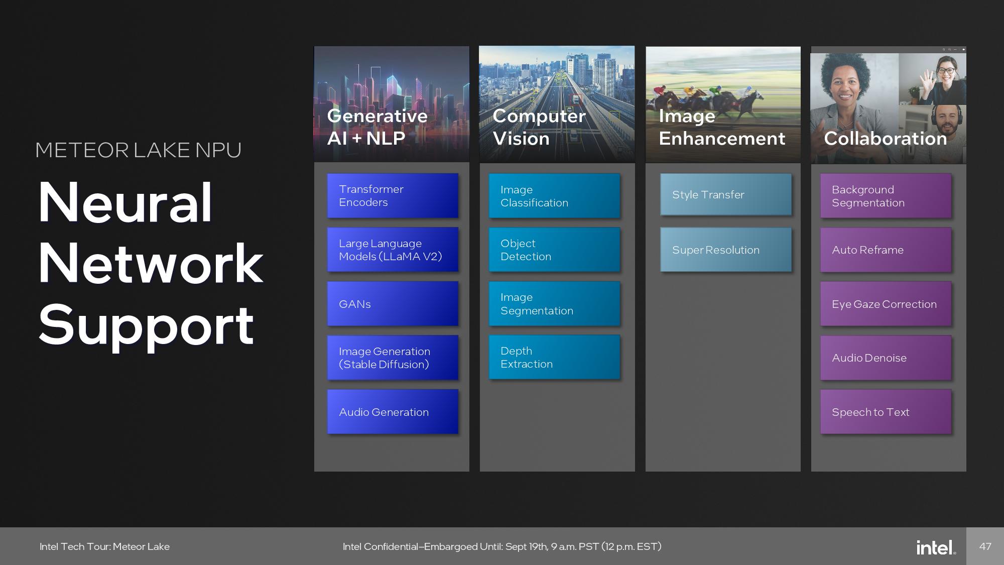
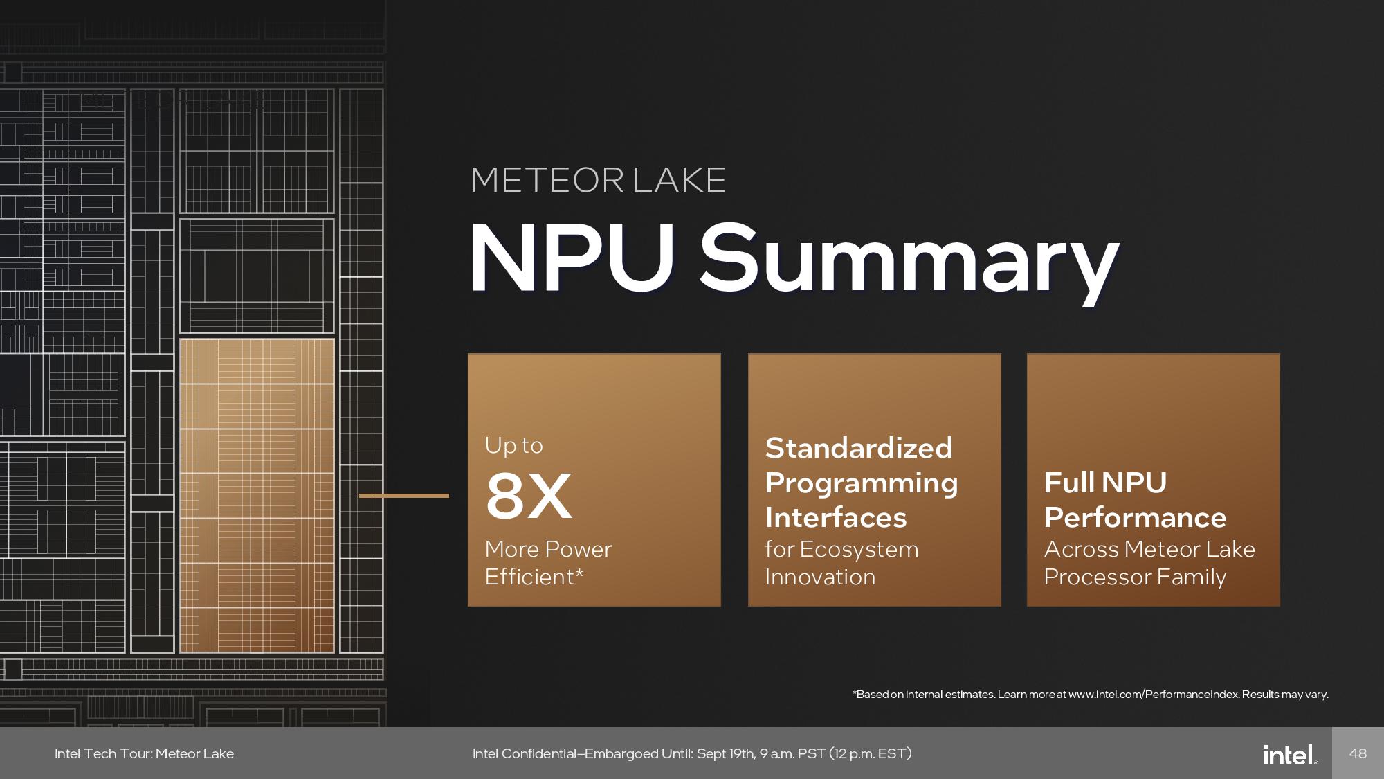
Intel’s neural processing unit (NPU) is a dedicated AI engine that’s designed specifically to run sustained AI inference workloads (not training), but Meteor Lake also includes a CPU, GPU, and GNA engine that can run other various AI workloads. The NPU is primarily for background tasks, while the GPU steps in for heavier parallelized work. Meanwhile, the CPU addresses light low-latency inference work.
Some AI workloads can also run on both the NPU and GPU simultaneously, and Intel has enabled mechanisms that allow developers to target the different compute layers based on the needs of the application at hand. This will ultimately result in higher performance at lower power – 8x less, in fact -- a key goal of using the AI acceleration NPU.
Many of today's more intense AI workloads, such as training large language models like ChatGPT and the like, require intense computational horsepower and will continue to run in data centers. However, Intel some AI applications, like audio, video, and image processing, will be addressed locally on the PC, which Intel says will improve latency, privacy, and cost.
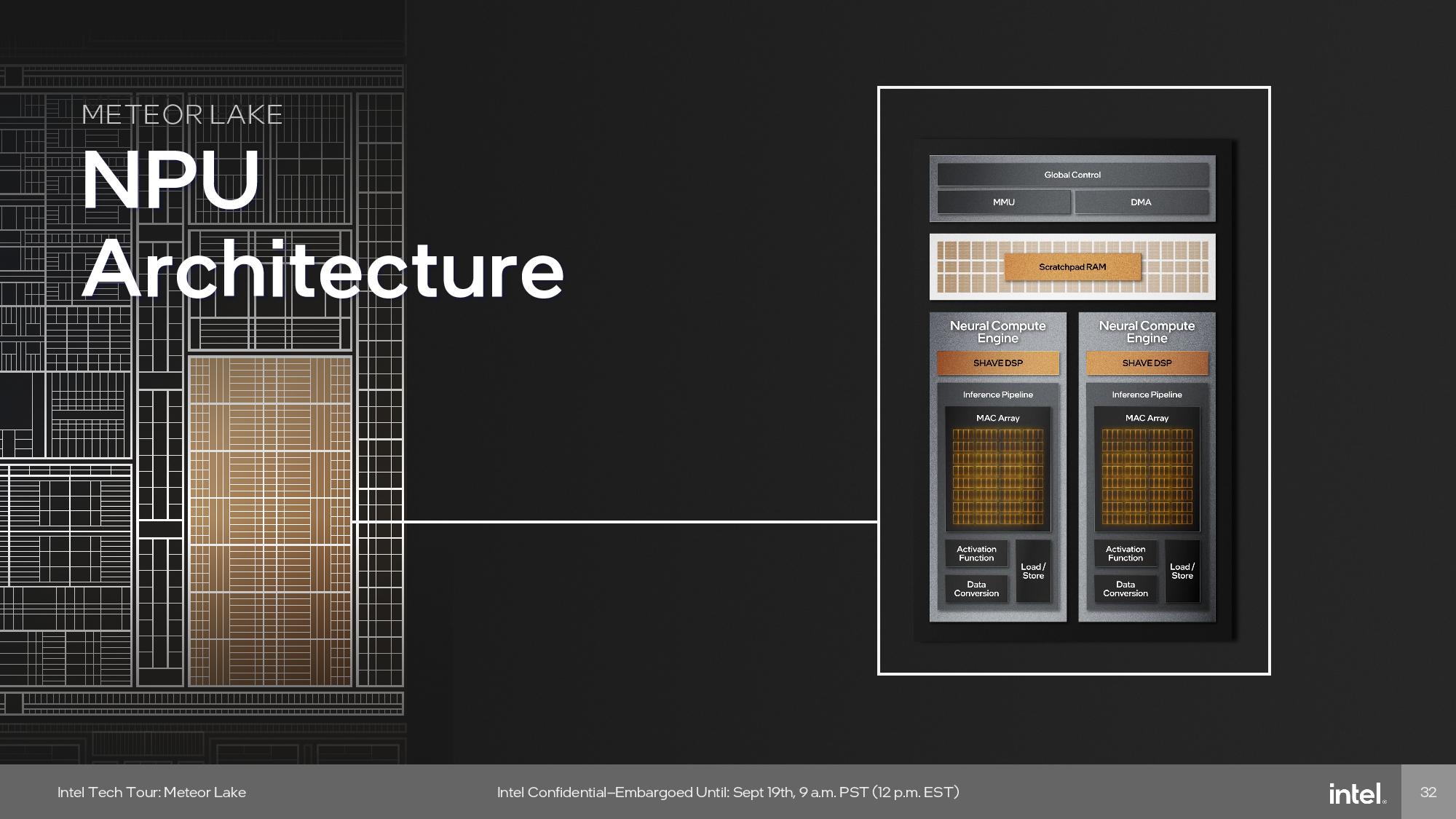
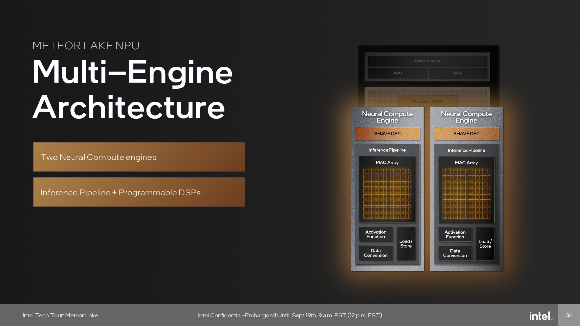
The NPU architecture contains a mix of fixed function accelerators for the inference pipelines, and programmable SHAVE DSPs. Here’s Intel’s description of the engine:
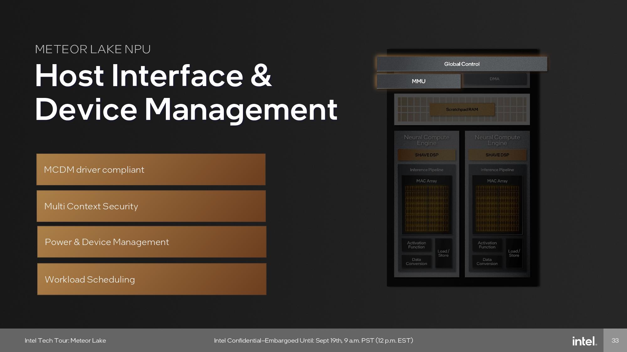
- Host Interface and Device Management – The device management area supports the new driver model from Microsoft called Microsoft compute driver model (MCDM). This enables the Meteor Lake NPU to support MCDM in an optimal way with a focus on security, while the Memory Management Unit (MMU) provides multi-context isolation and supports power and workload scheduling forfast, low-power-state transitions.
- Multi–Engine Architecture – The NPU consists of a multi-engine architecture with two neural compute engines that work together on a single workload or work independently on their own workloads. Within this neural compute engine there are two main compute components:
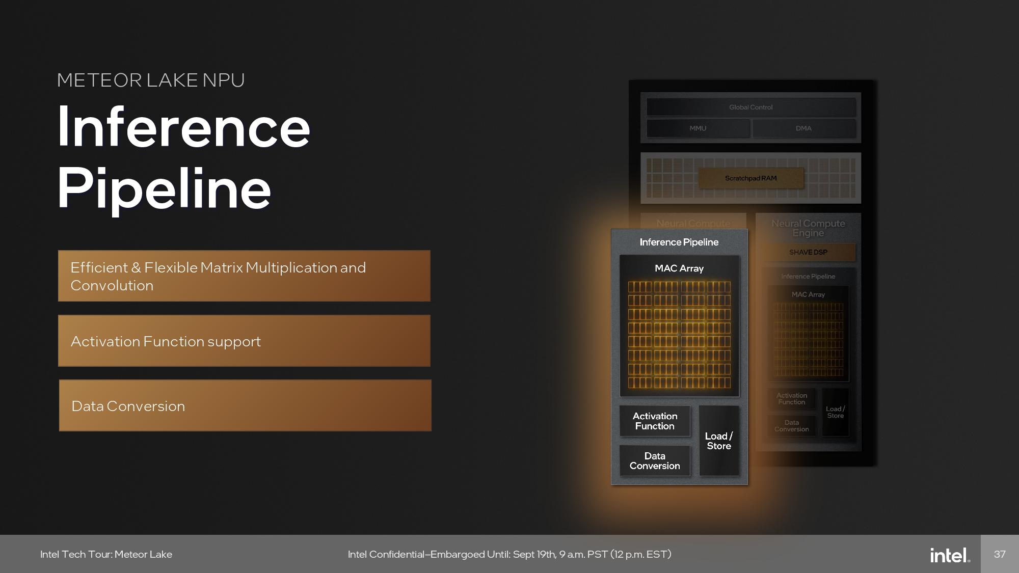
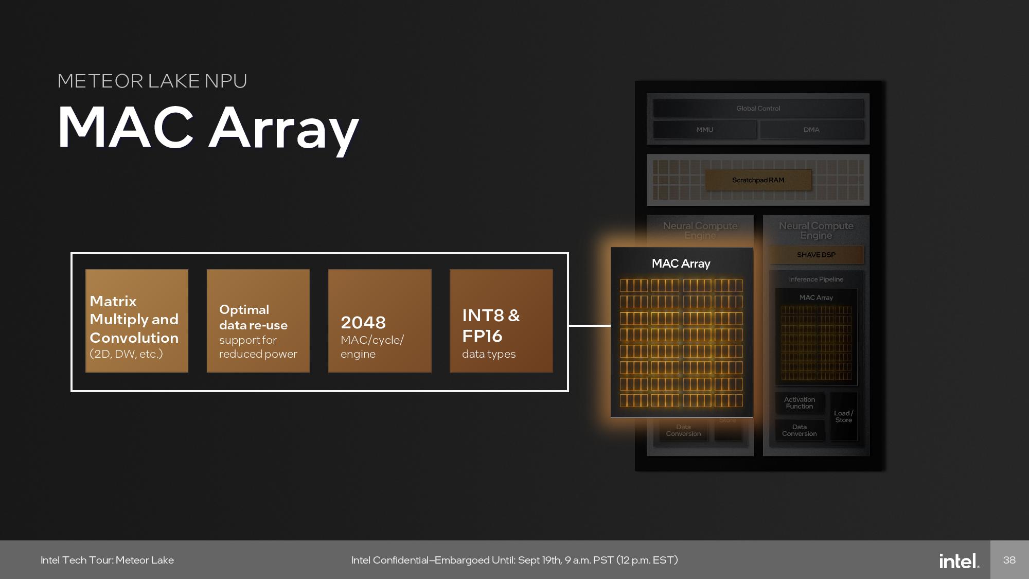
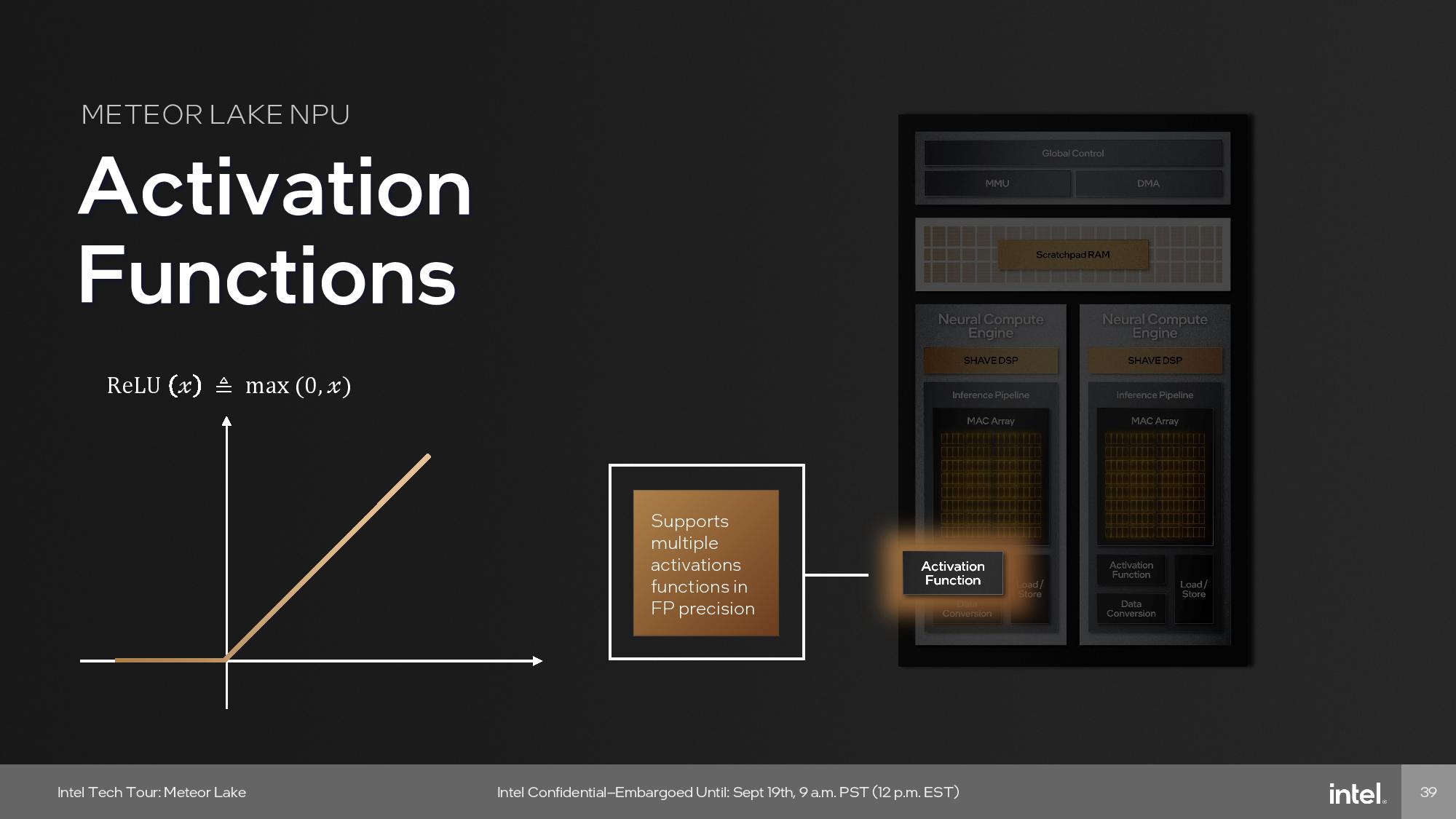
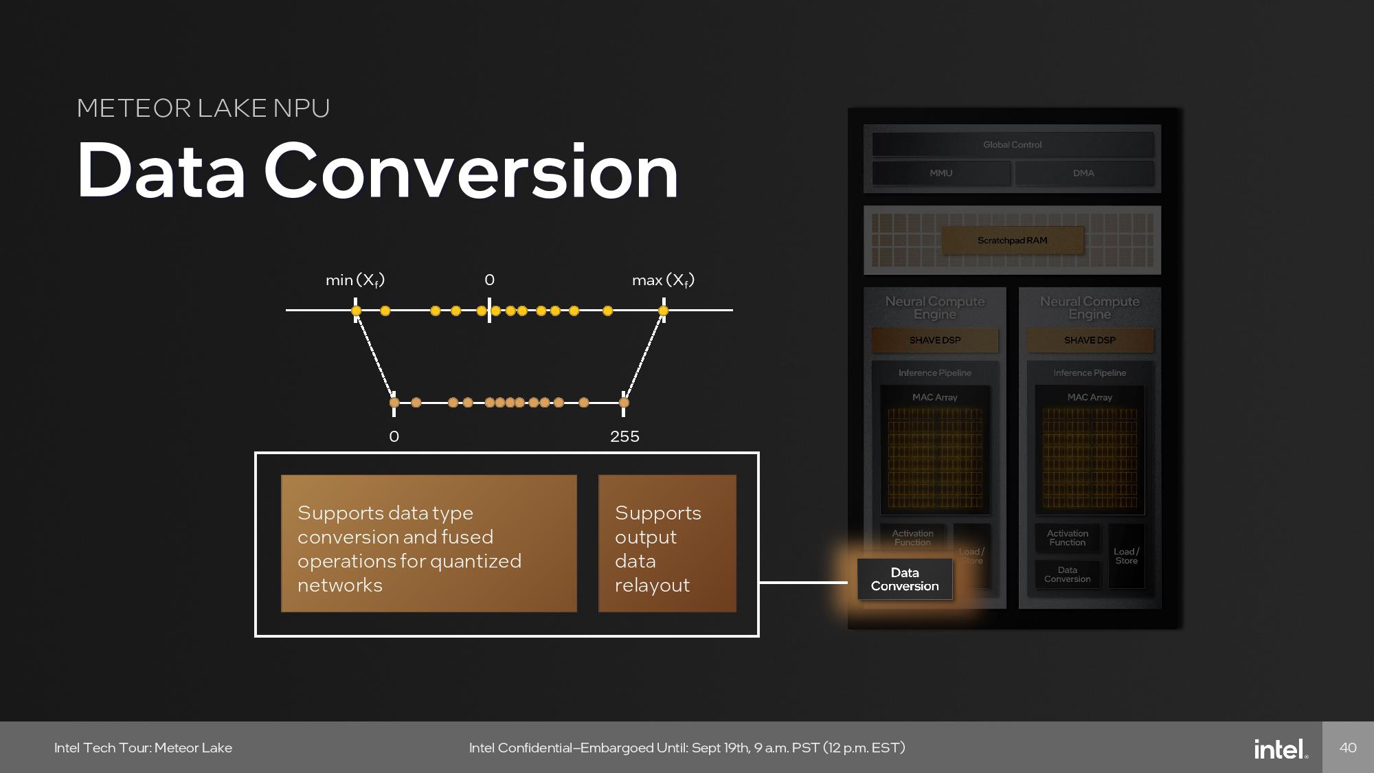
- Inference Pipeline – This is the core driver of efficient computing that saves power in a neural network execution by minimizing data movement and having fixed function operations for common and high-compute tasks. The majority of compute happens on the inference pipeline, a pipeline of fixed function hardware supporting standard neural network operations. The pipeline consists of a Multiply Accumulate (MAC) array, an activation function block, and a data conversion block.
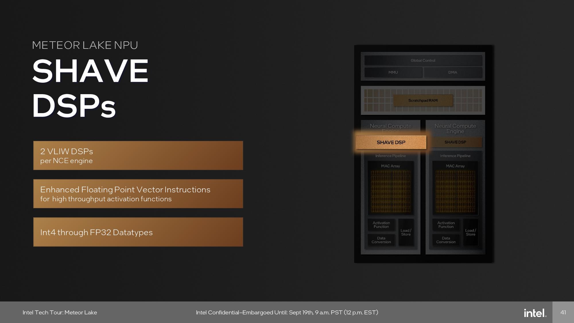
- SHAVE DSP – This is a highly optimized VLIW DSP (Very Long Instruction Word/Digital Signal Processor) designed specifically for AI. The Streaming Hybrid Architecture Vector Engine (SHAVE) can be pipelined with the inference pipeline and Direct Memory Access (DMA) engine for true heterogenous compute that happens in parallel on NPU to maximize performance.
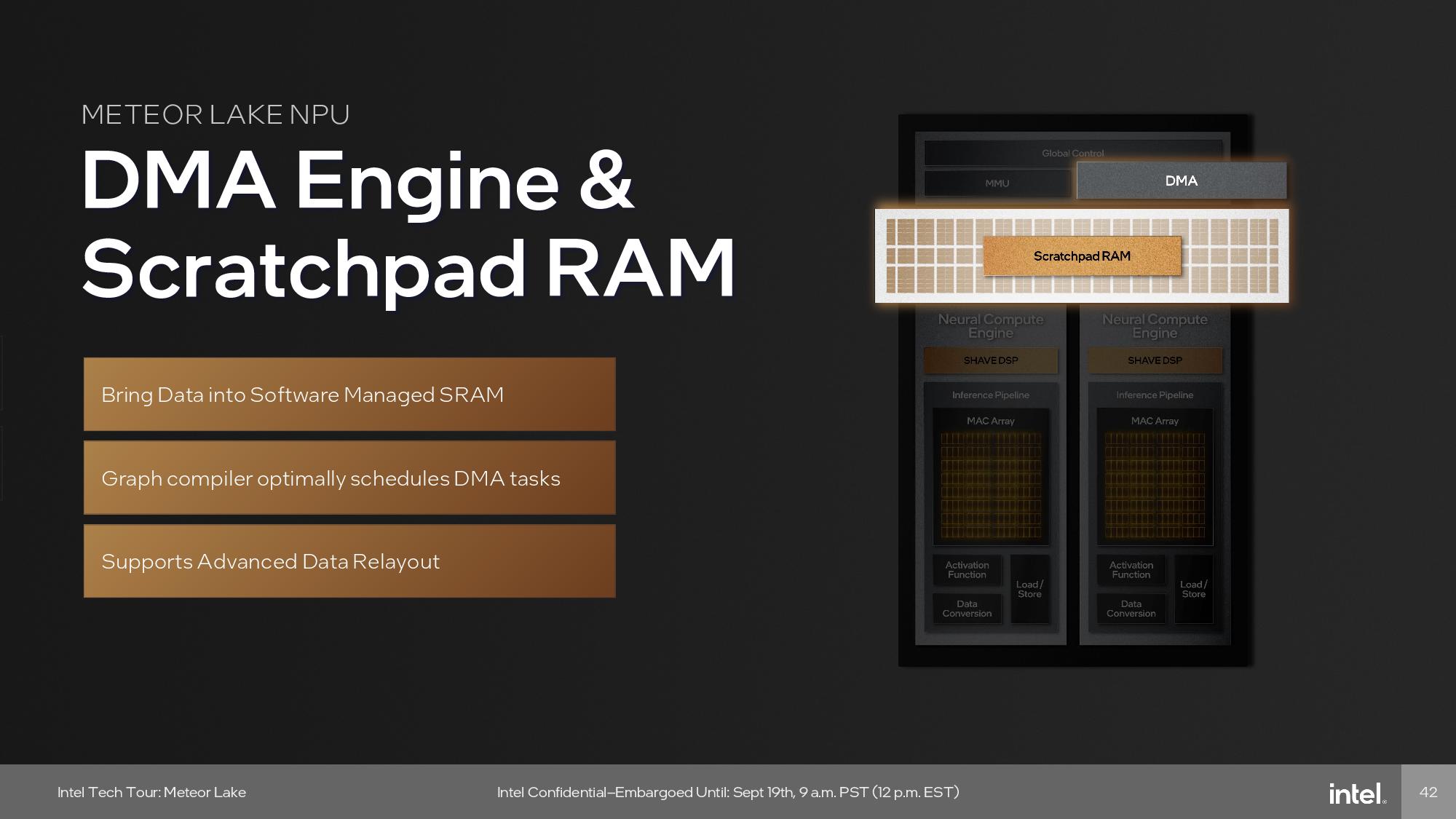
- DMA Engine – This optimally orchestrates data movement for maximum efficiency and performance.
Intel's chips currently use a gaussian neural accelerator (GNA) block for low-power AI inference for audio and video processing functions, and the GNA unit will remain on Meteor Lake. However, Intel says it is already running some of the GNA-focused code on the NPU and achieving better results, with a heavy implication that Intel will transition to the NPU entirely with future chips and remove the GNA engine.
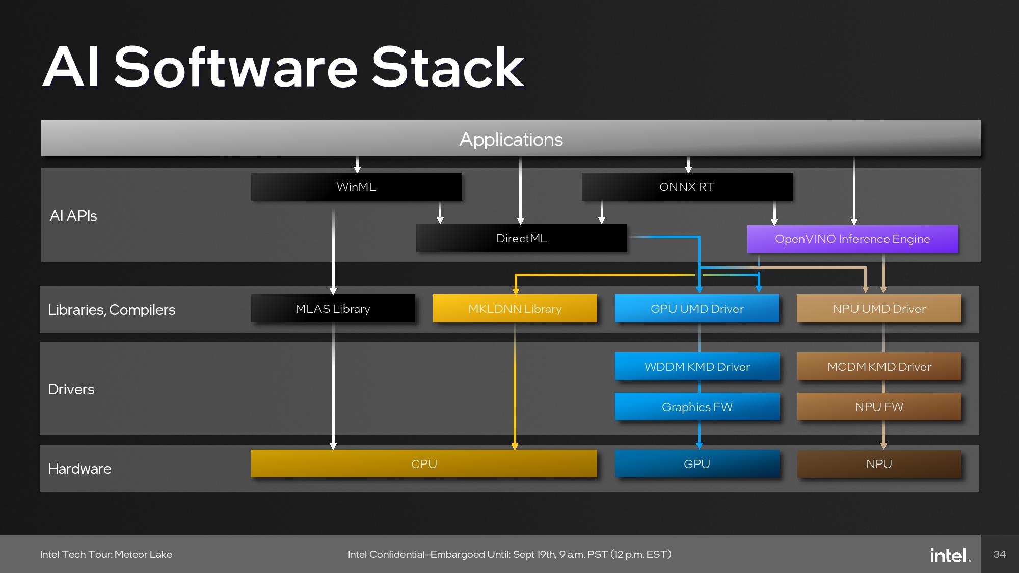
Intel's NPU supports DIrectML, but also ONNX and OpenVINO, which Intel says offers better performance on its silicon. However, ONNX and OpenVINO will require more targeted development work from software devs to extract the utmost performance.



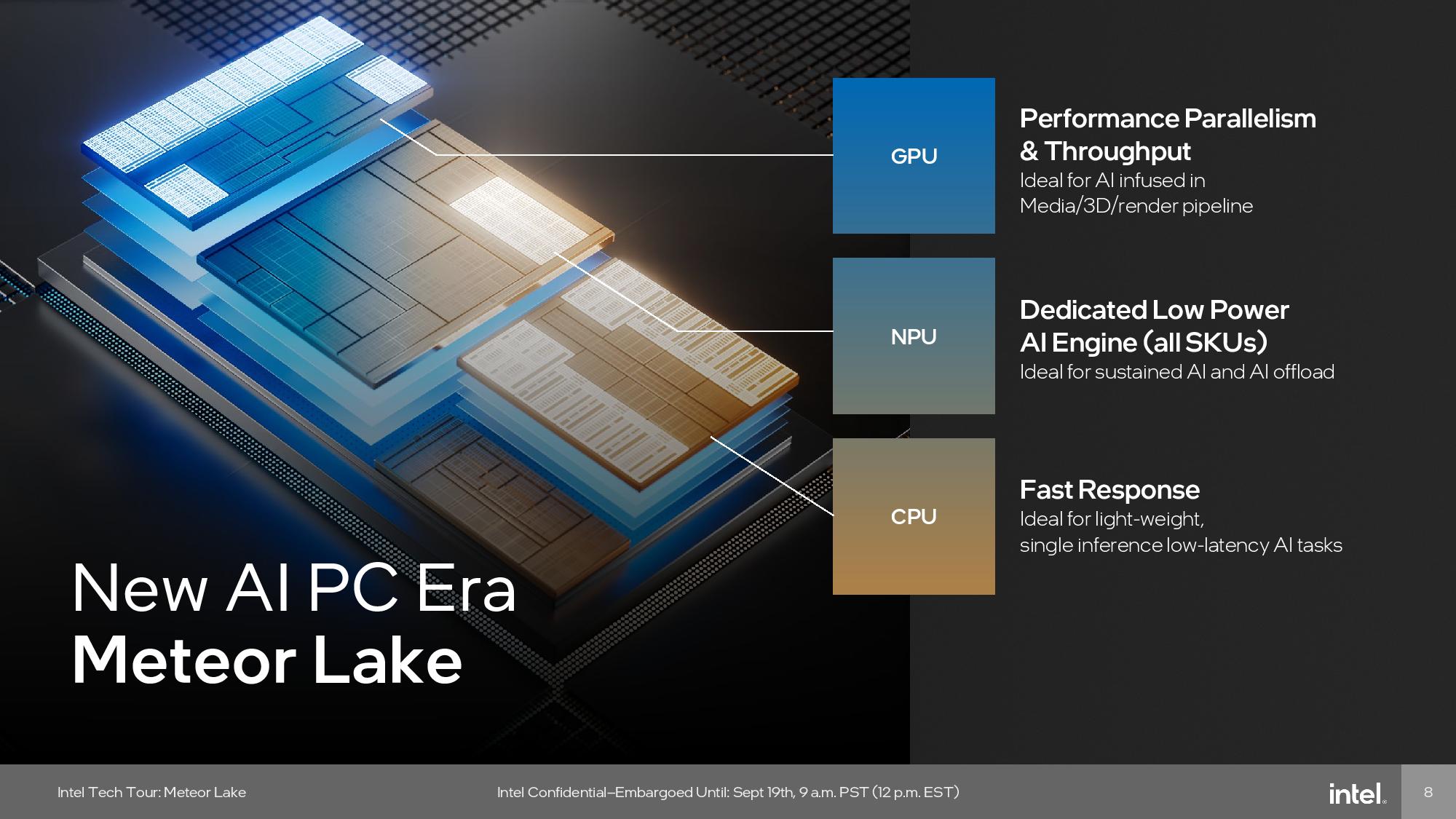
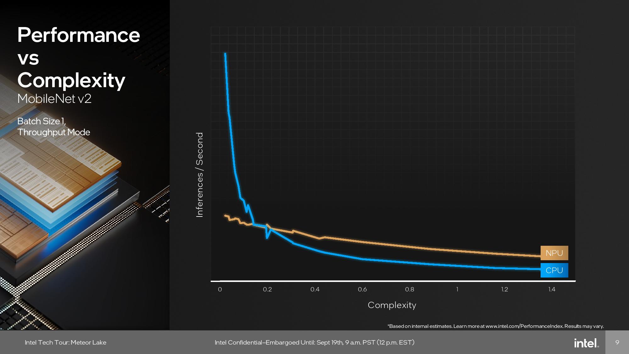
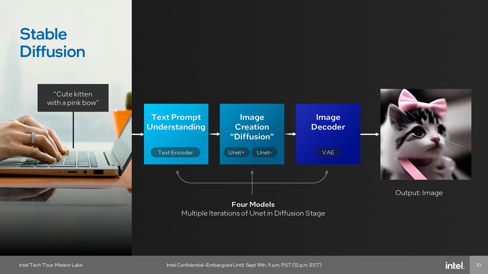
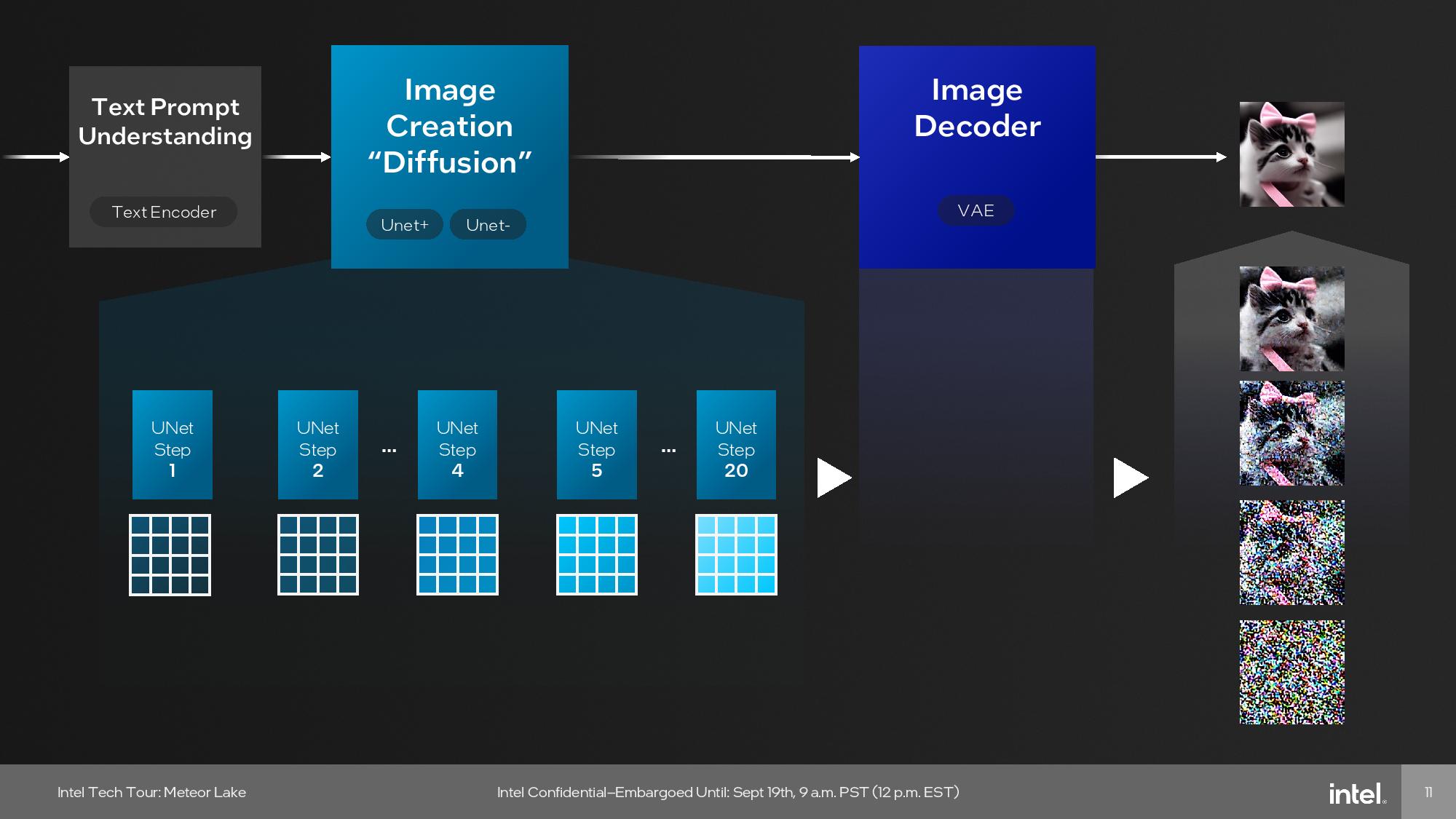
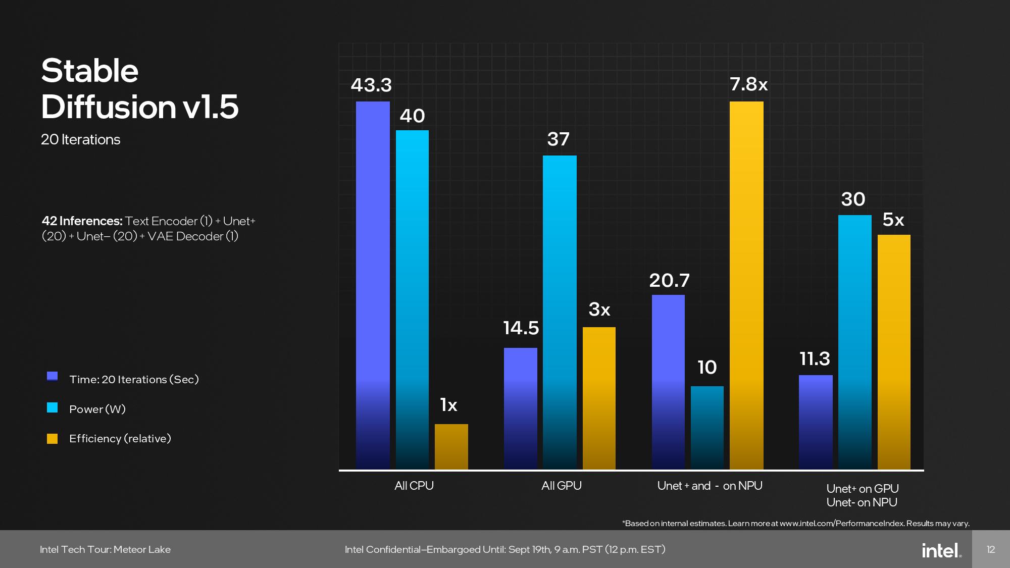
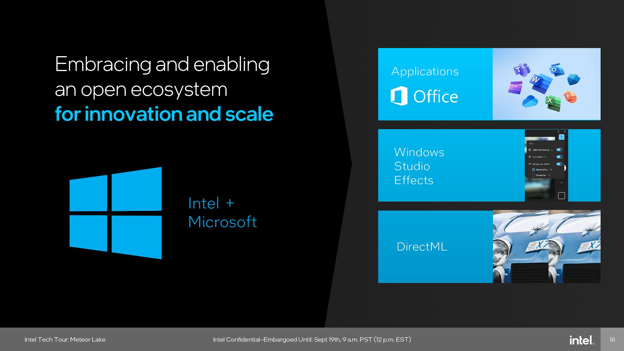
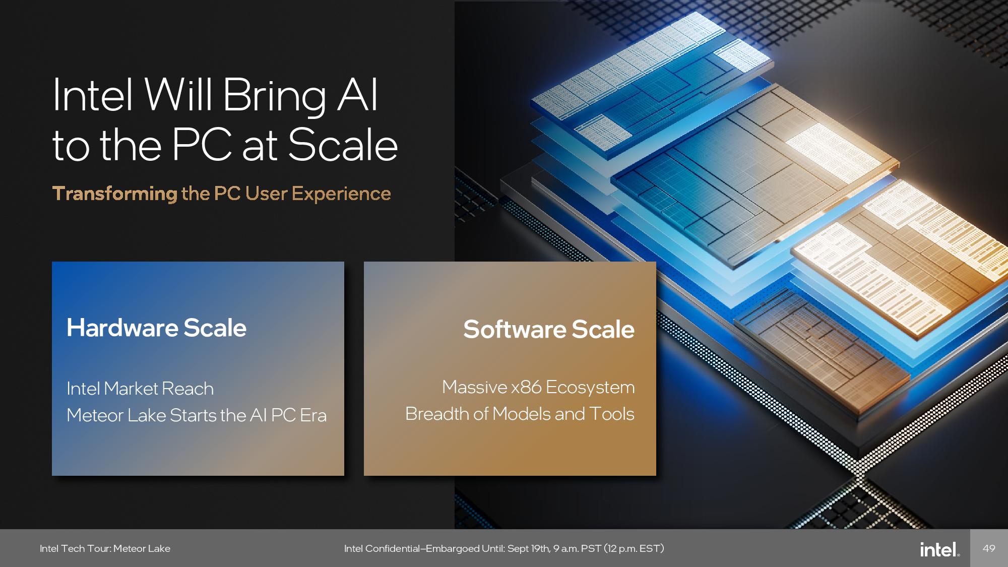
The nascent PC AI software ecosystem is now moving more quickly to accommodate the new dedicated AI engines present not only in Intel’s chips, but also in AMD’s competing Ryzen 7040-series processors that already have their own dedicated AI engines. However, there aren’t currently many mainstream applications -- for now, it’s a chicken and egg situation. Intel plans to bring its NPU to tens of millions of devices by 2025, and with AMD also making similar design decisions, we can expect the software enablement efforts to accelerate.
Foveros 3D Packaging
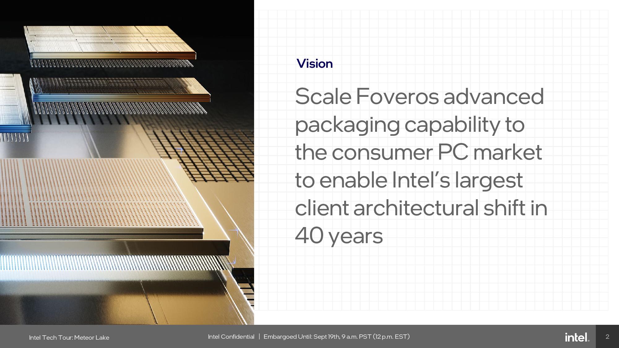

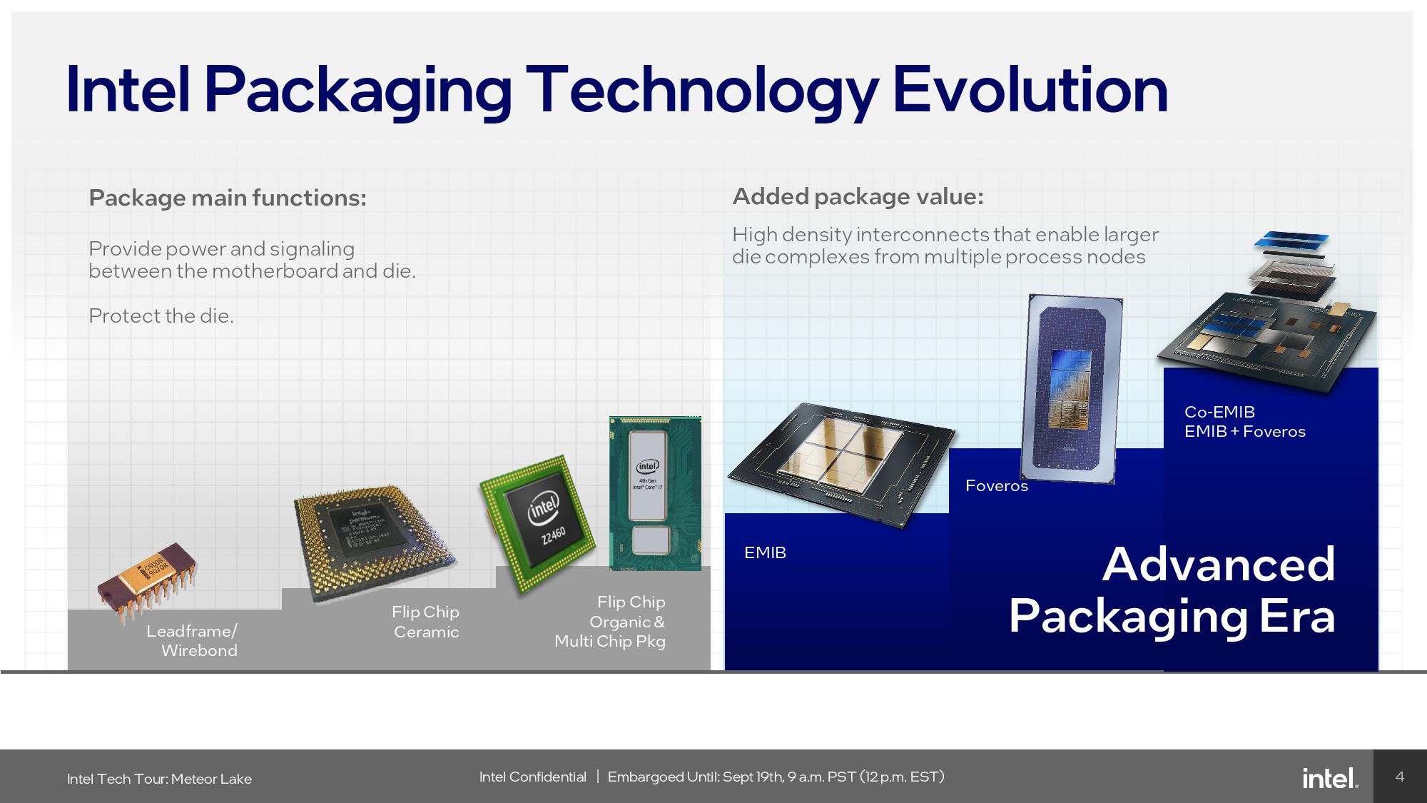
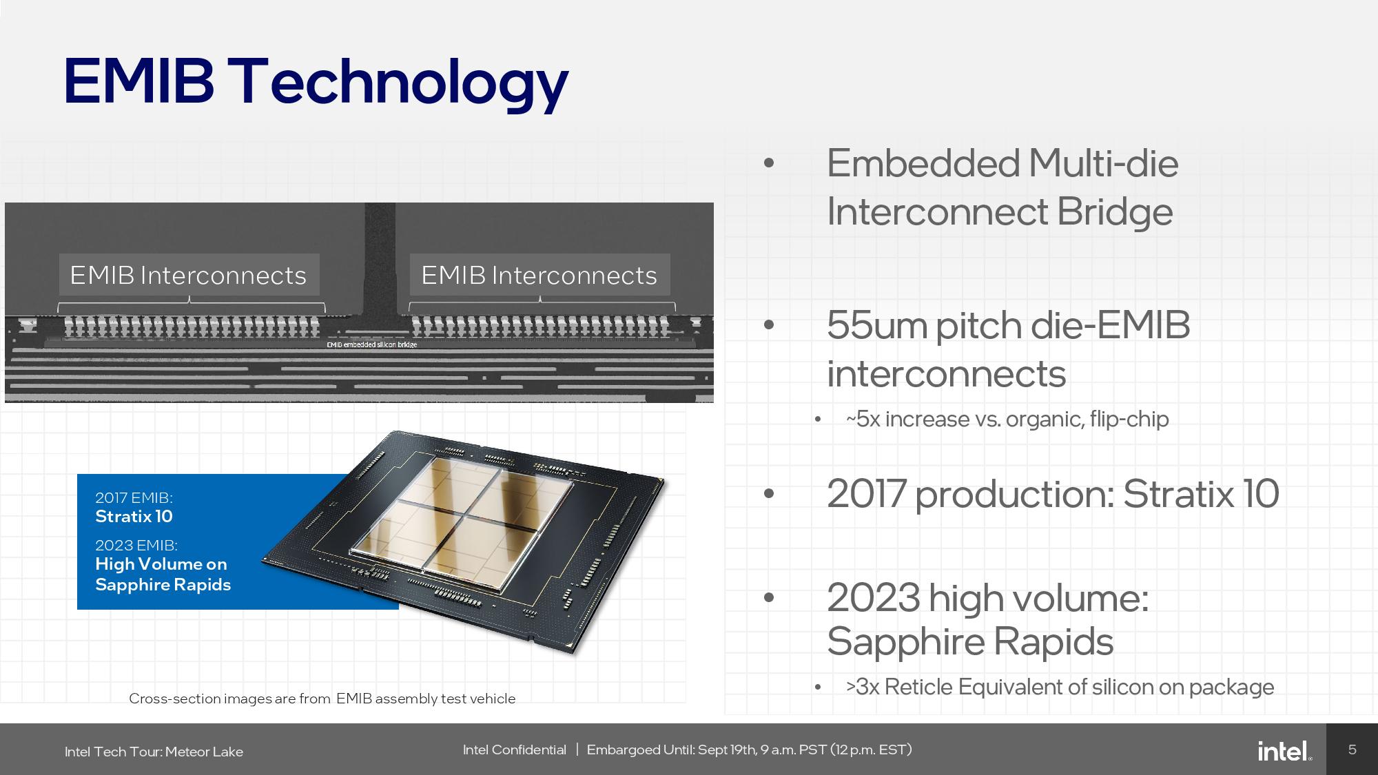
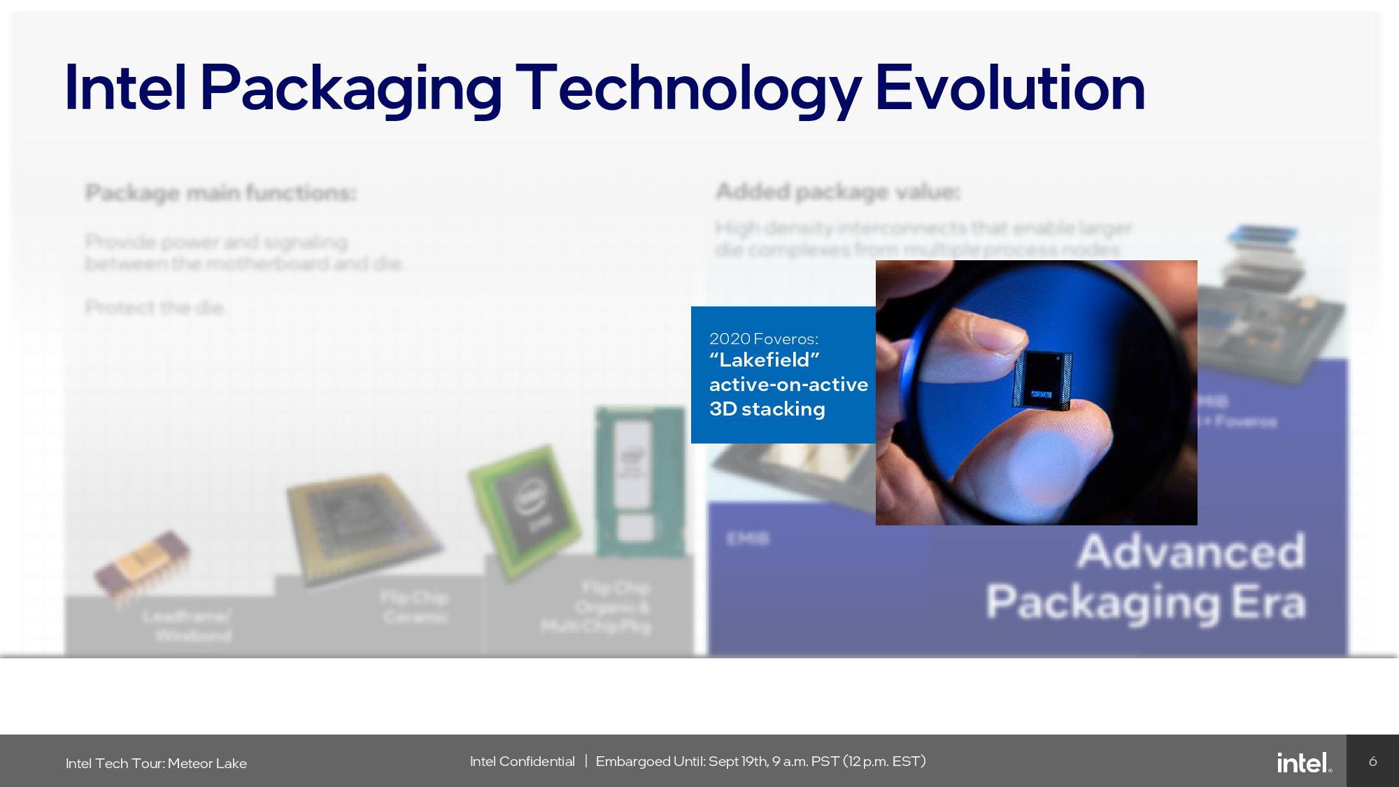
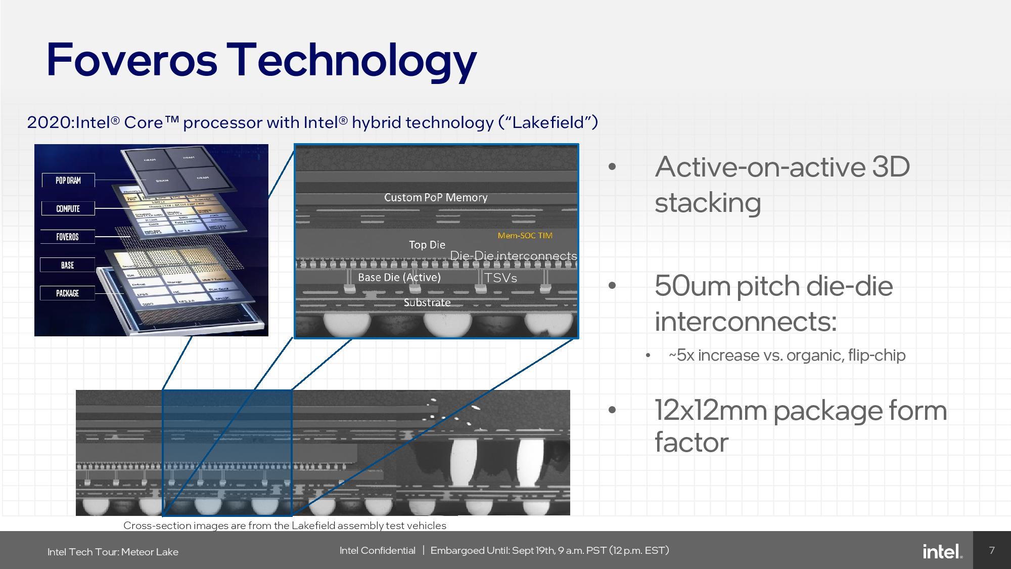
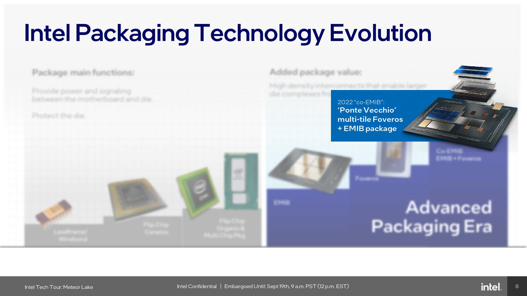
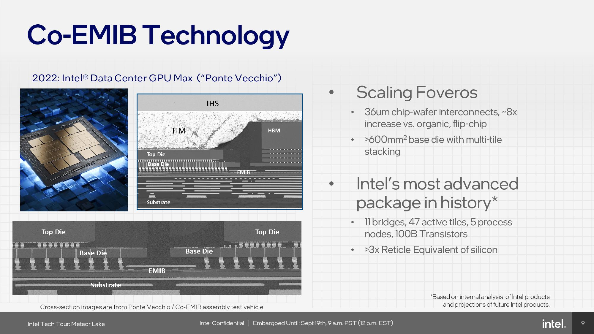
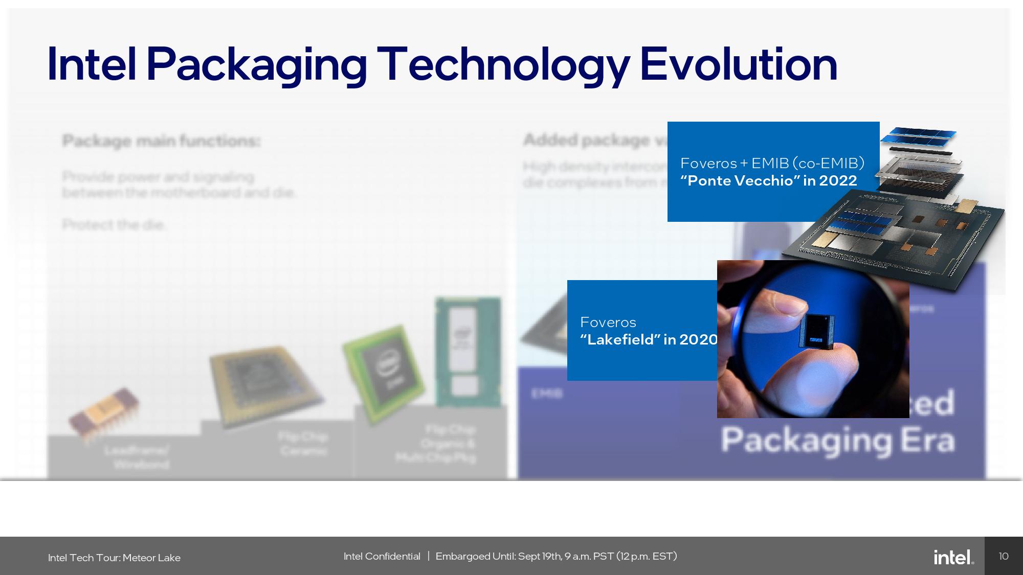
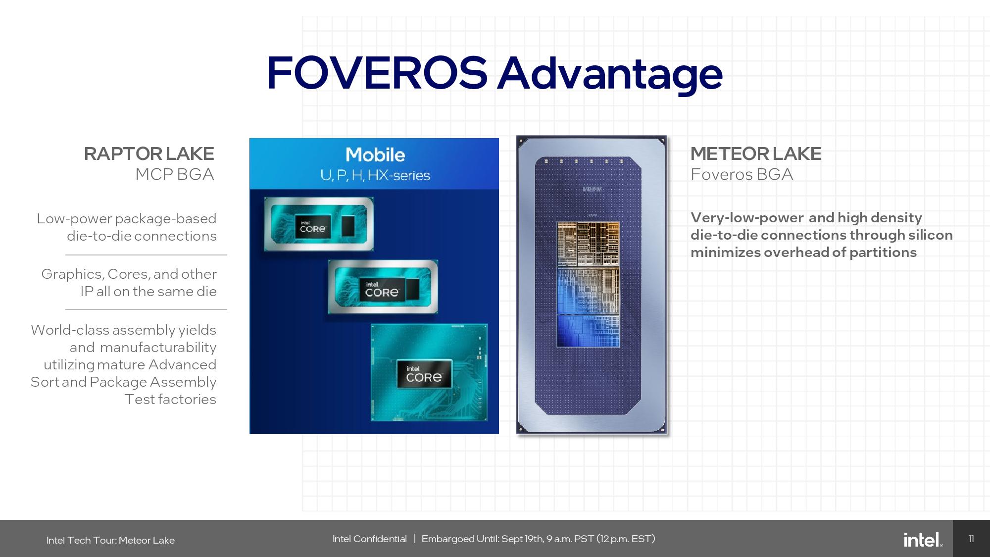
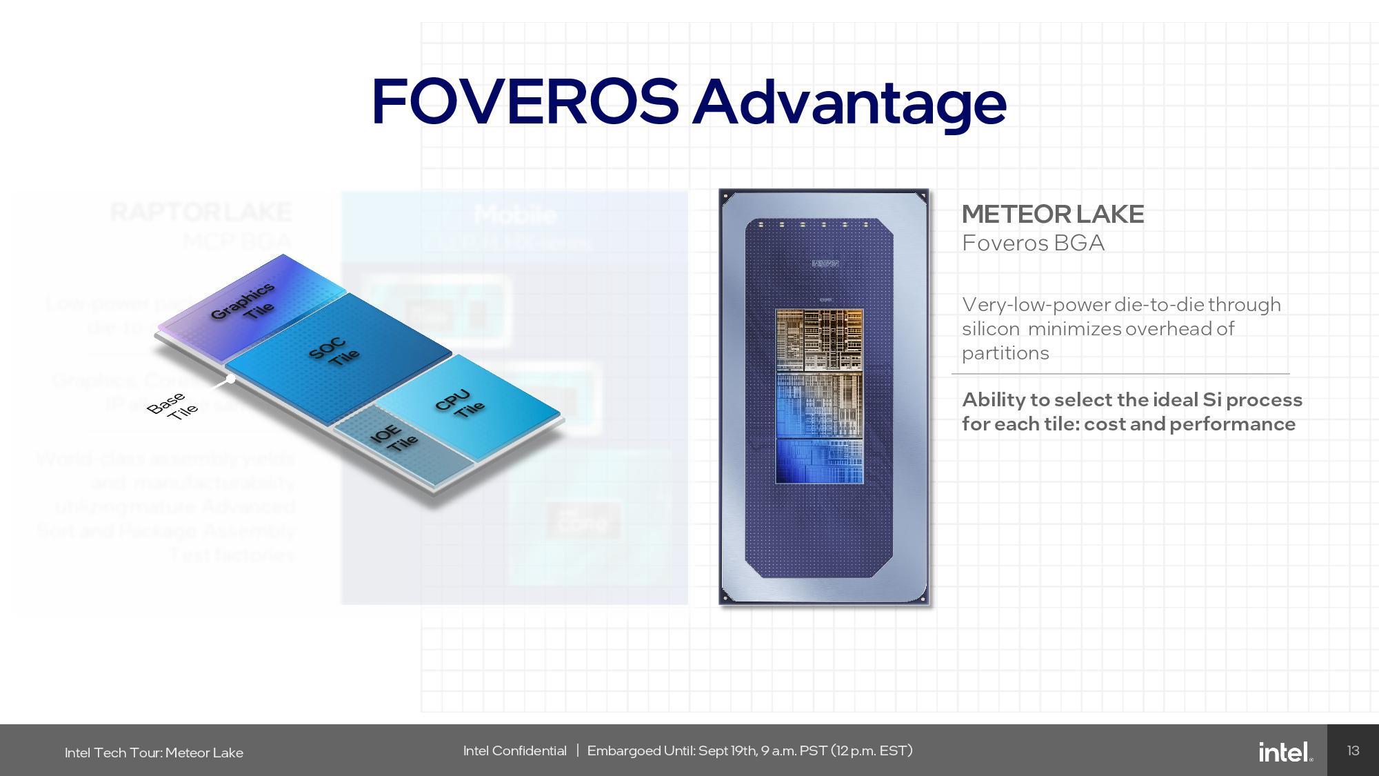
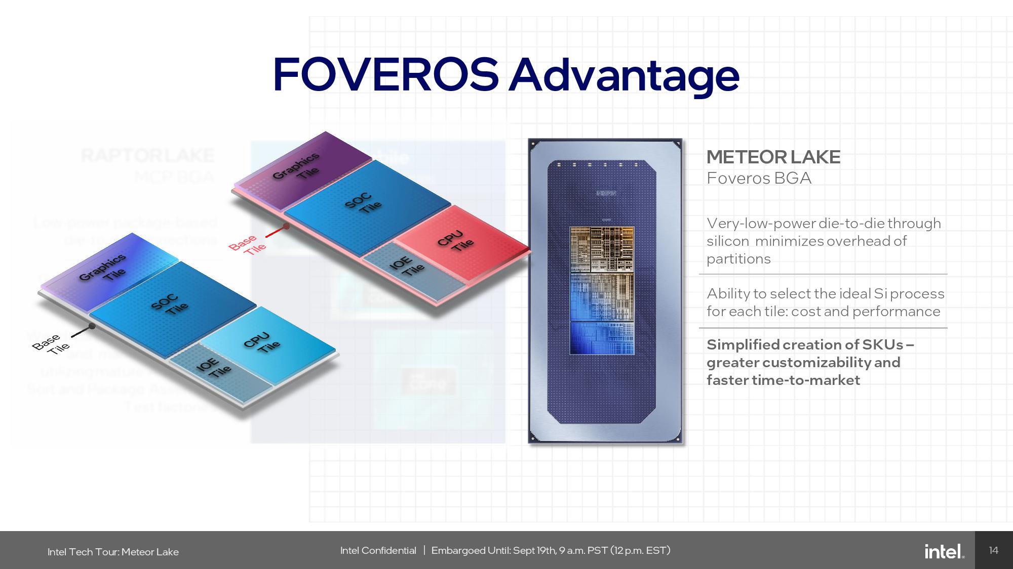
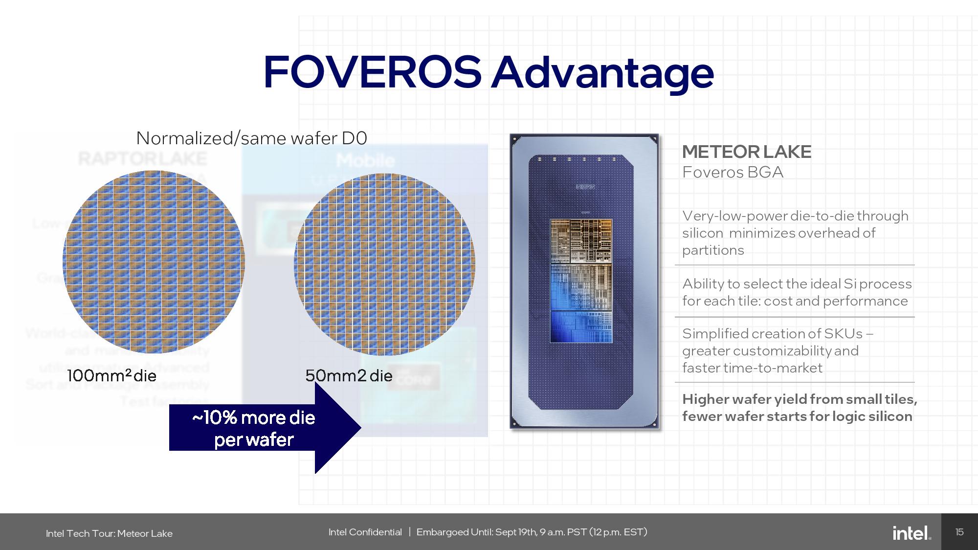

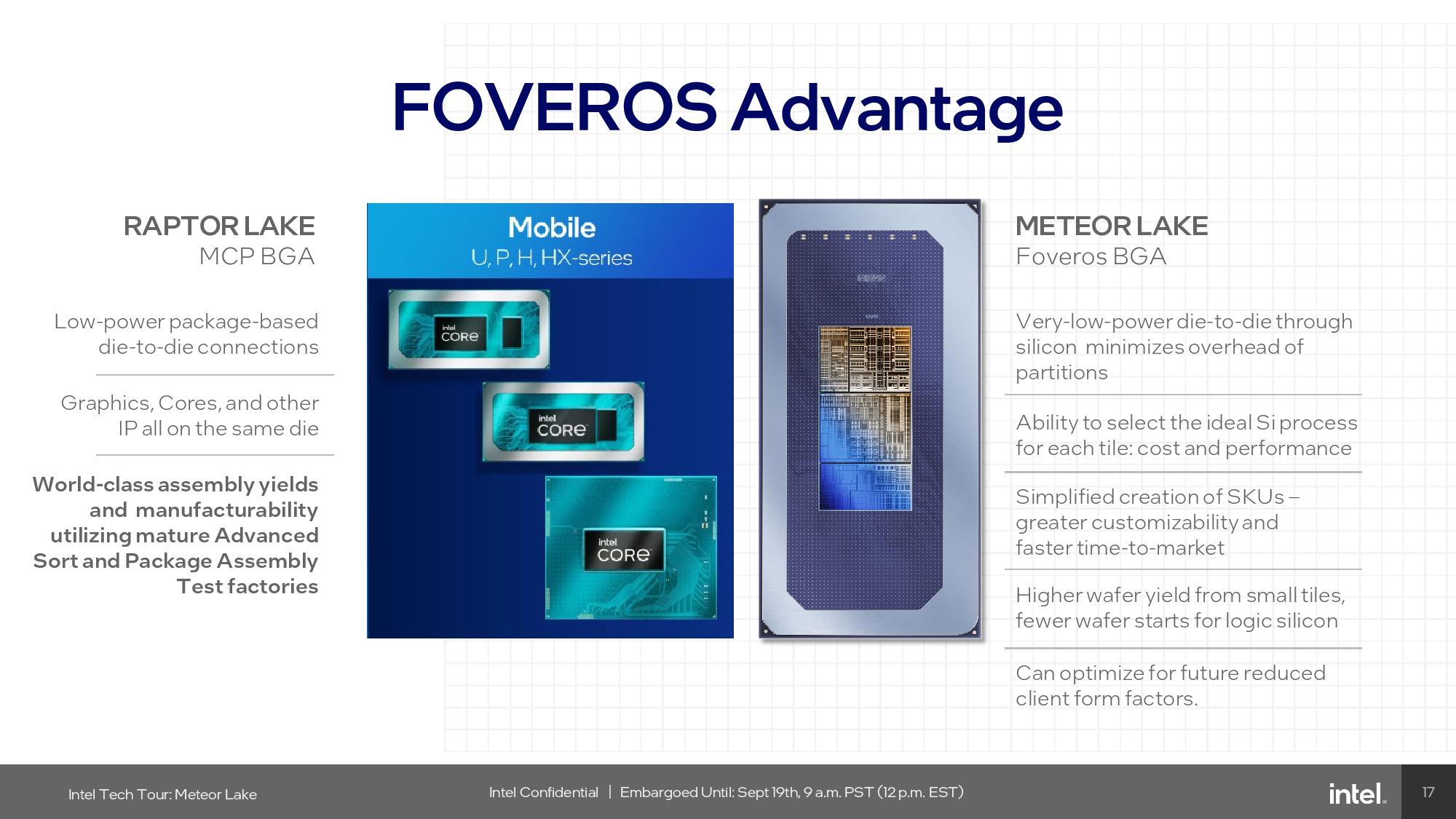
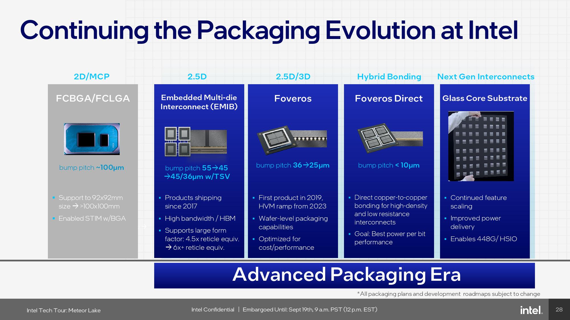
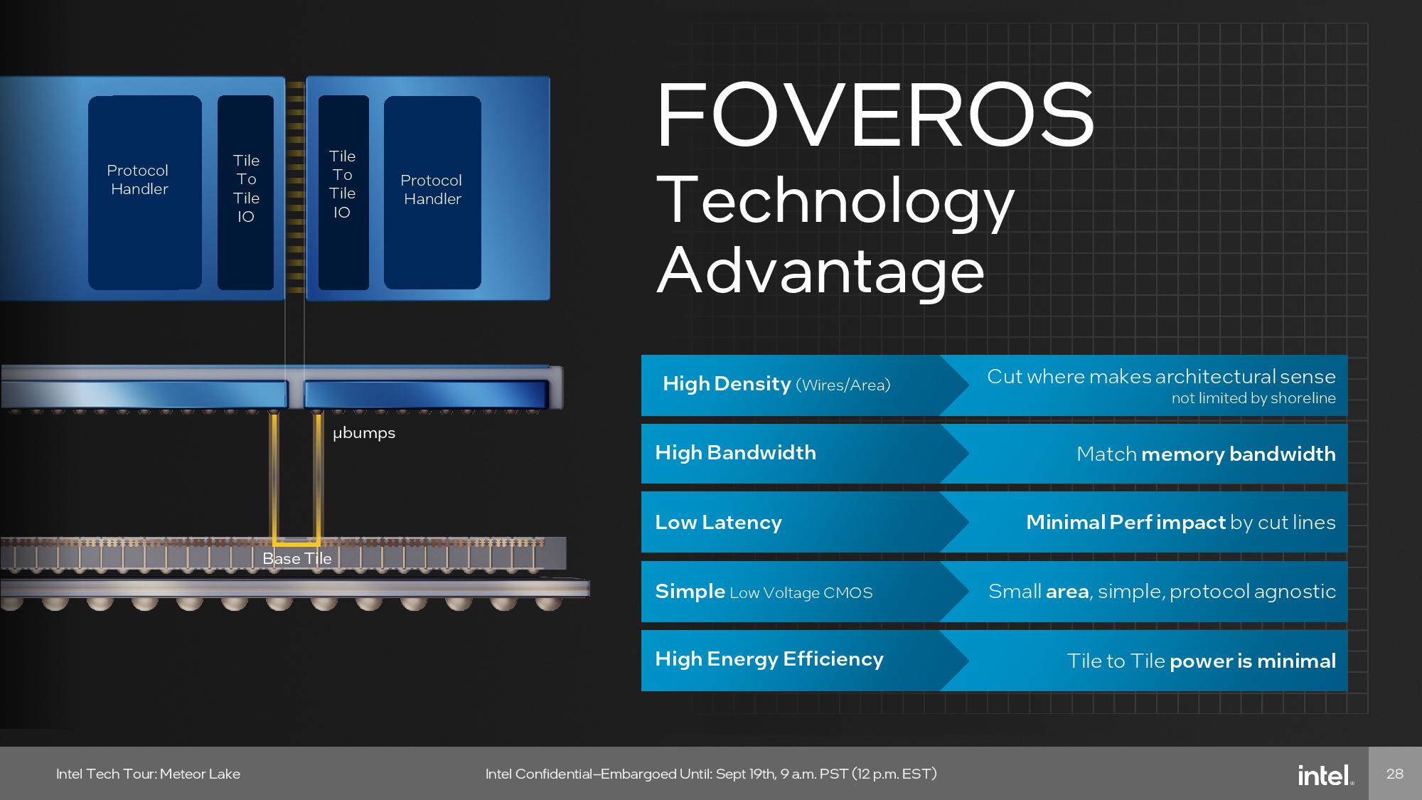
Packaging and interconnect advancements are rapidly changing the face of modern processors. Both are now just as important as the underlying process node technology — and arguably more important in some facets, as they allow mixing and matching different types of process nodes within a single package to extract the best blend of performance, power consumption, and cost.
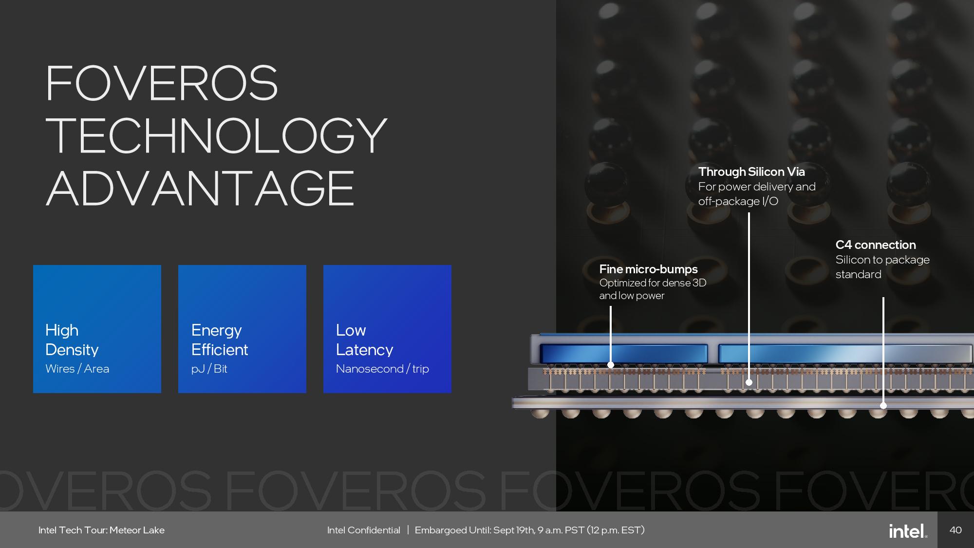
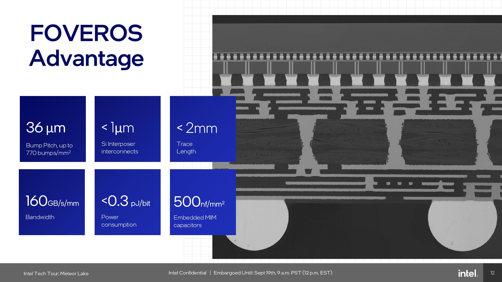
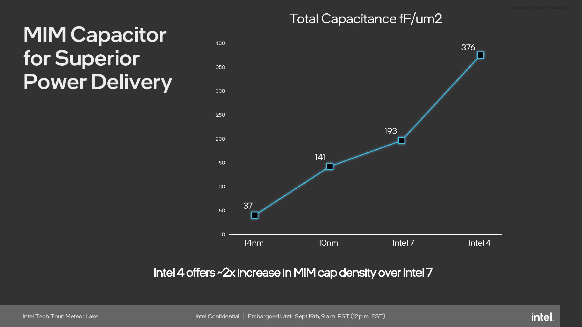
Intel manufactures the Foveros interposer with its low-cost and low-power-optimized 22FFL process. Intel places the four Meteor Lake tiles on top of a passive Foveros 3D interposer/base tile, and the tiles and interposer are then fused together with microbump connections that enable high-speed communications and efficient power delivery. The passive interposer doesn’t have any logic, so it doesn’t perform any type of processing work and mostly serves as a high-speed pathway for communication between tiles. However, it does have embedded MIM capacitors (500nf/mm^2) that help ensure steady power delivery to the tiles during periods of heavy load.
Foveros uses a 36-micron bump pitch (a critical measurement of interconnect density), an improvement over the 55-micron bump pitch it used with Lakefield (the first Foveros chips). For now, Foveros enables up to 770 microbumps per square millimeter, but that will improve drastically in the future: The Foveros roadmap includes 25- and 18-micron pitches with future designs. In the future, Intel says it could theoretically even use hybrid bonding interconnects (HBI) to reach 1-micron bump pitches.
| Interconnect | Picojoules per Bit (pJ/b) |
| NVLink-C2C | 1.3 pJ/b |
| UCIe | 0.5 - 0.25 pJ/b |
| Infinity Fabric | ~1.5 pJ/b |
| TSMC CoWoS | 0.56 pJ/b |
| Foveros | Sub-0.3 pJ/b |
| EMIB | 0.3 pJ/b |
| Bunch of Wires (BoW) | 0.7 to 0.5 pJ/b |
| On-die | 0.1 pJ/b |
Foveros is also very power efficient, delivering among the best energy efficiency of any off-die interconnect at <0.3 picojoules per bit (pJ/b). The interposer’s high-density connections also allow Intel to partition its tiles without worrying about the shoreline issues it encountered with external I/O interfaces. Intel designed the Foveros die to be as low-cost as possible and still deliver on the company's electrical and performance goals — it's the cheapest die on the Meteor Lake package by orders of magnitude.
Intel says the Foveros interconnect/base tile supports up to 160GB/s per mm, so bandwidth will scale with additional interconnects (the interfaces can run at 'multiple GHz'). As such, Foveros doesn't incur any significant bandwidth or latency constraints that require design tradeoffs.
Overall, Intel feels that any tradeoffs with the Foveros technology are worth the trouble, as the interface is incredibly fast and sips power. It also has other tertiary benefits, like allowing the use of smaller chiplets that can boost the number of dies harvested per wafer by 10%, a boon for reducing overall costs. Intel also says the packaging technology behind Foveros is, on the whole, drop-in compatible with its existing production flows, another win as it looks to boost its packaging production capacity by 4x by the end of 2025.
At the end of the day, advanced packaging tech is used to mimic the key performance and power characteristics of a monolithic die, but with a chiplet-based architecture. Intel thinks Foveros is the winning formula that meets those goals.
Intel 4 Process Node
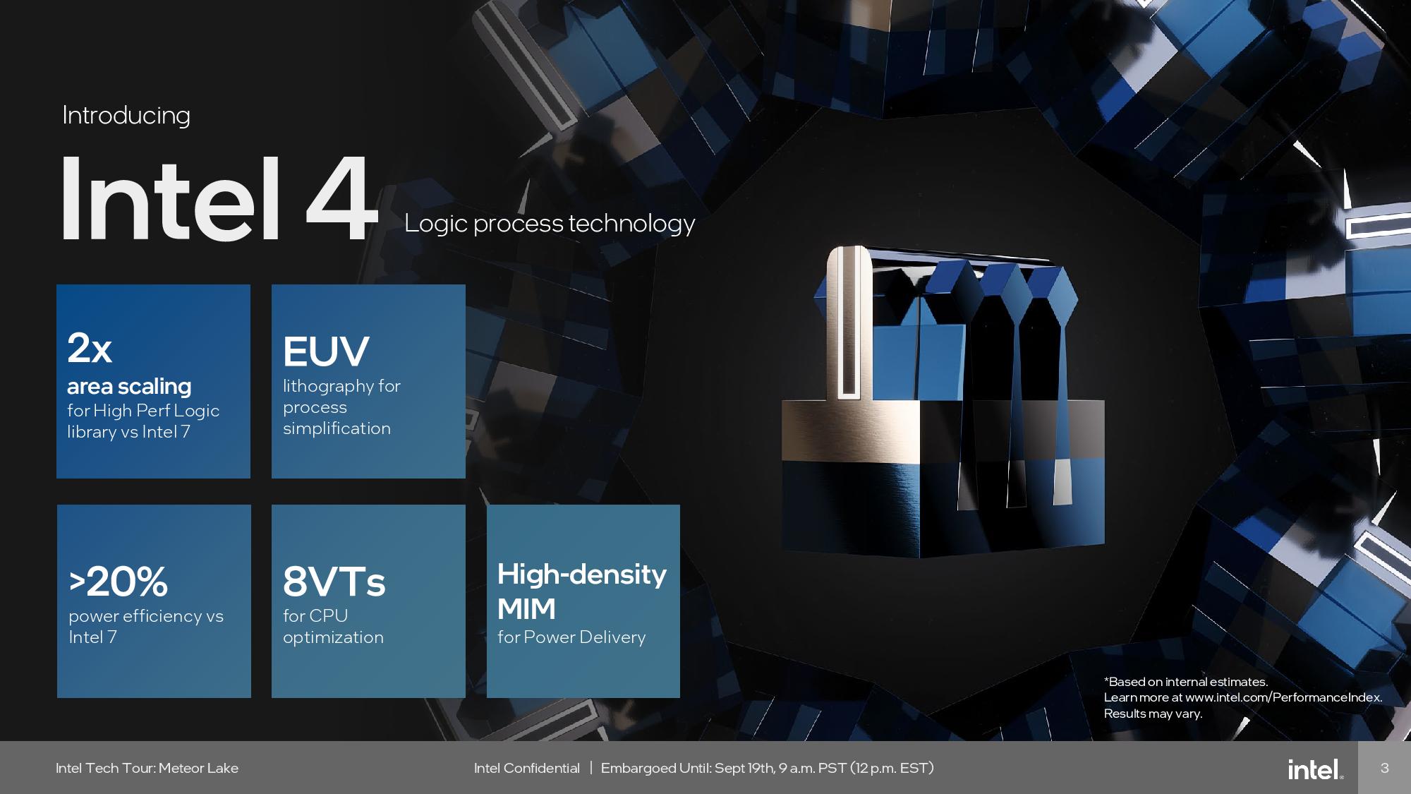


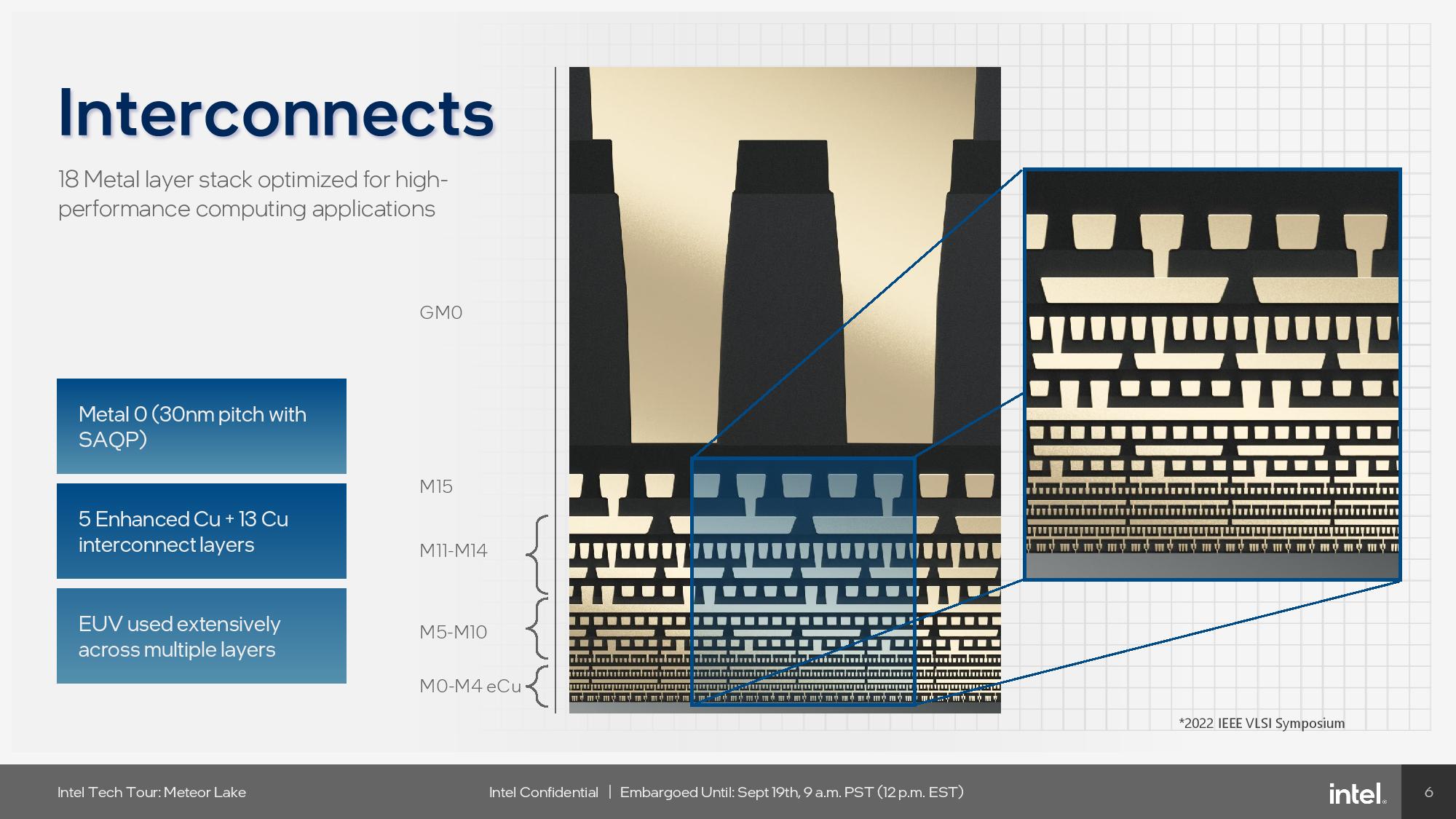
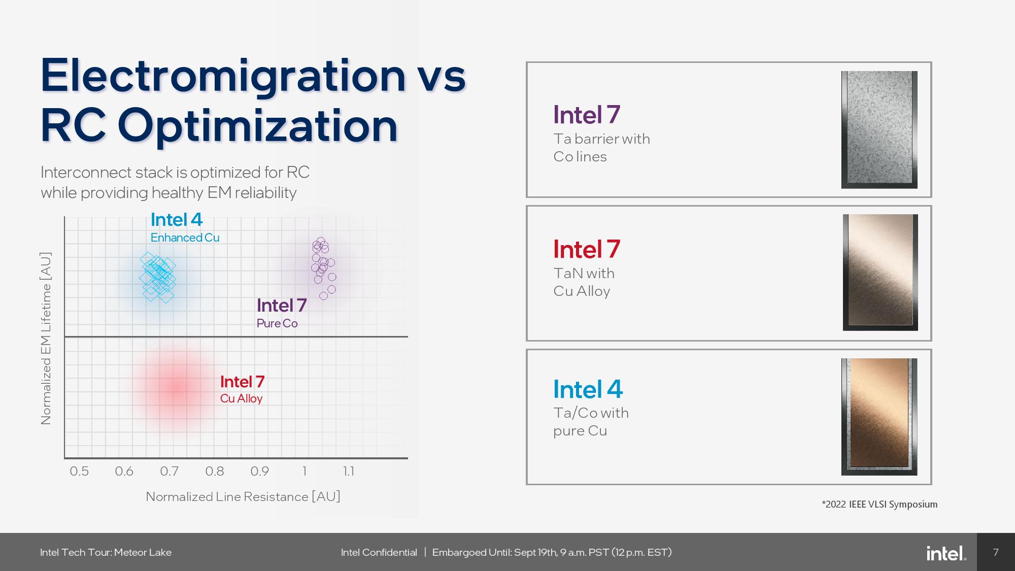


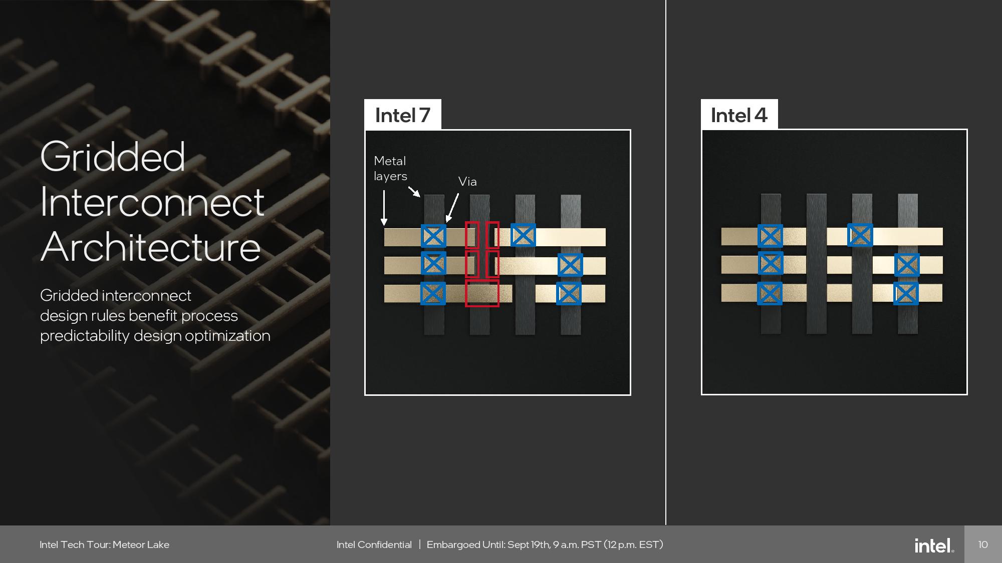

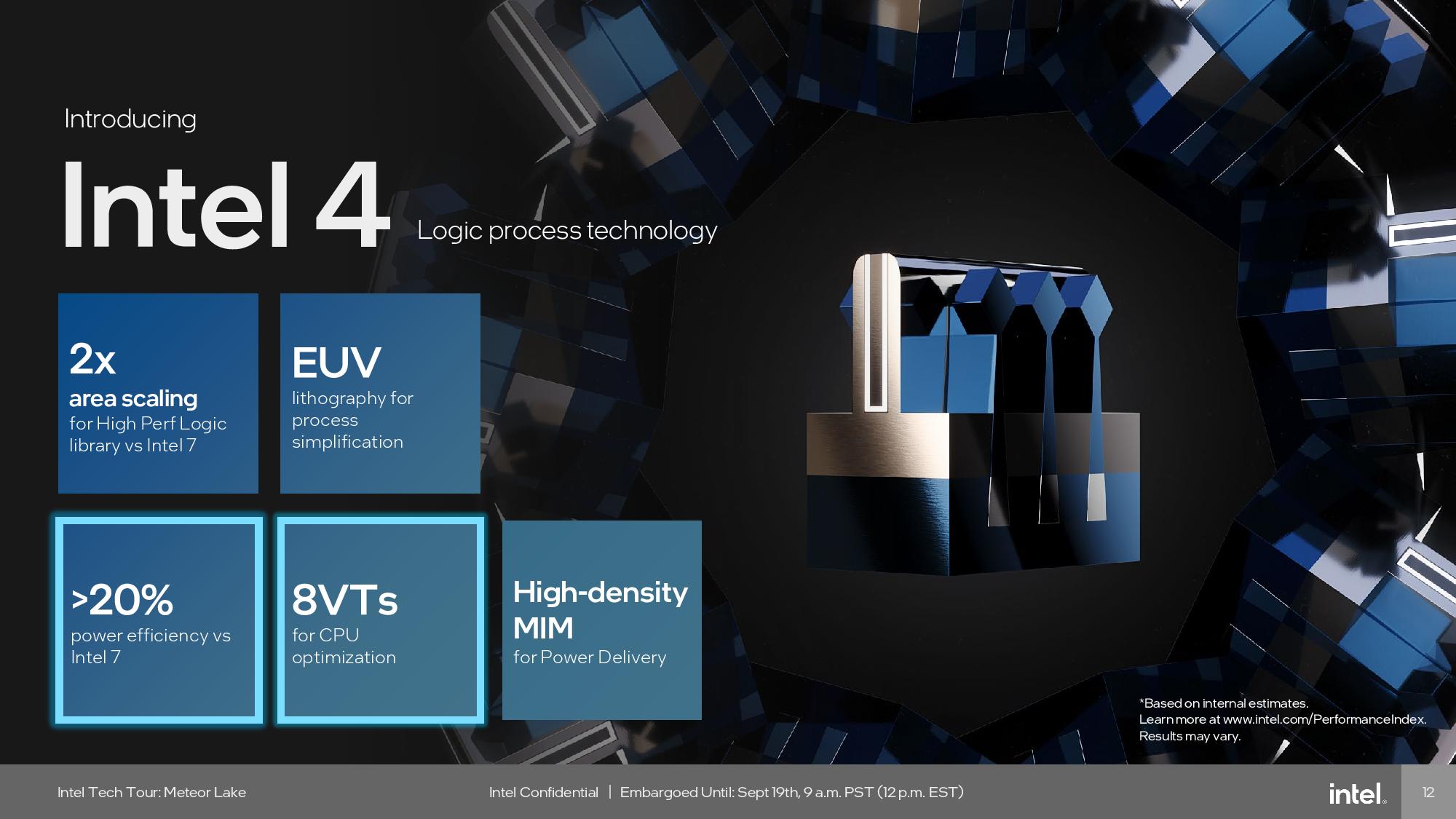
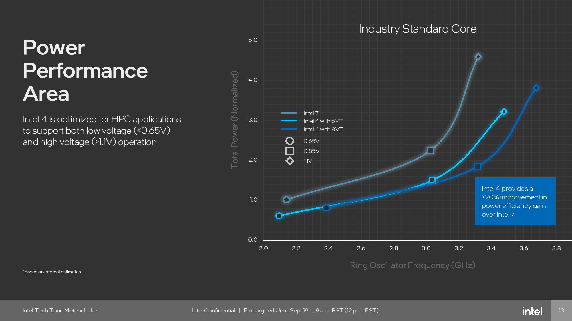
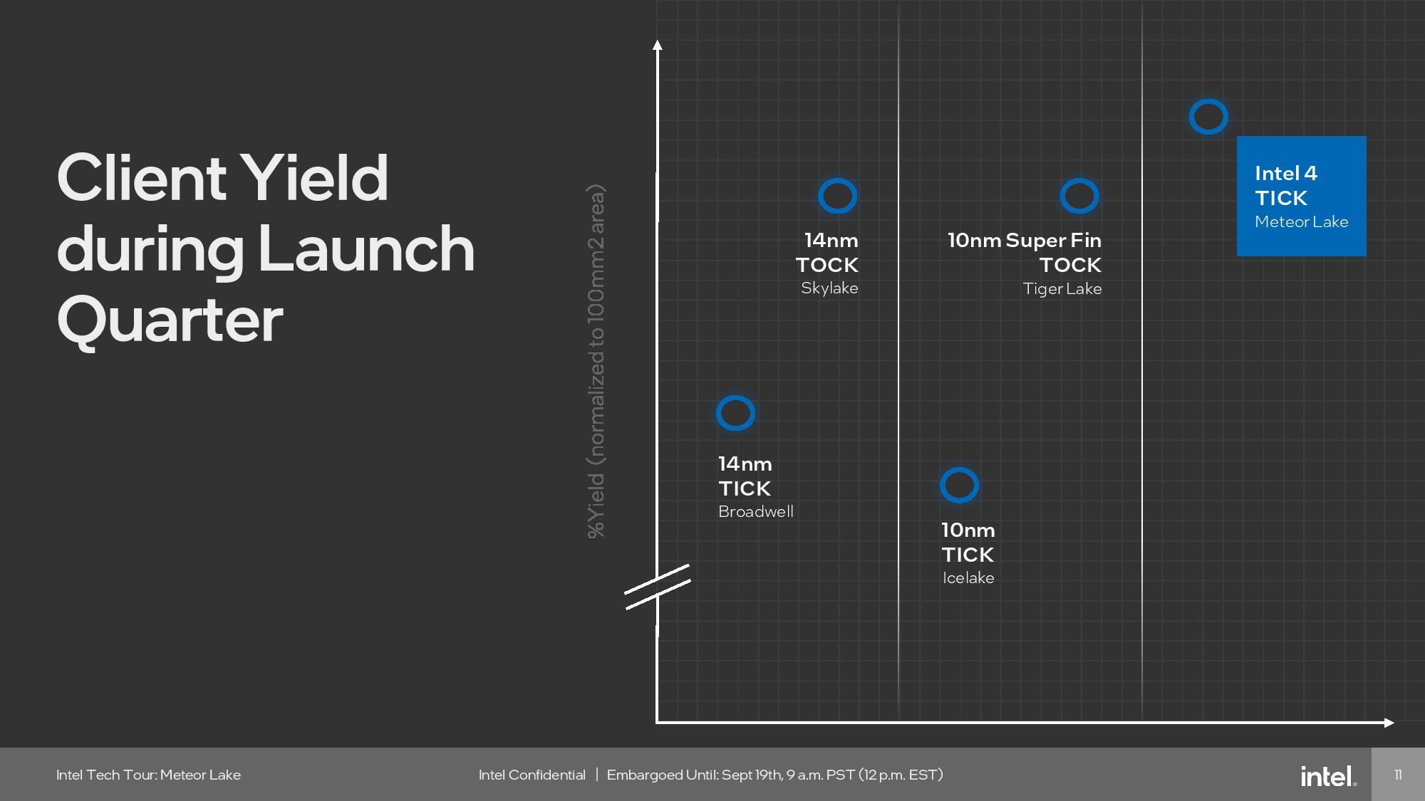
The Intel 4 process node is moving along well as it makes its way to high volume production: Intel representatives told us that this is the best-yielding node on day zero (the first wafers run through the fab) that the company has had in the last decade. The second slide shows that improvement relative to Intel’s prior nodes.
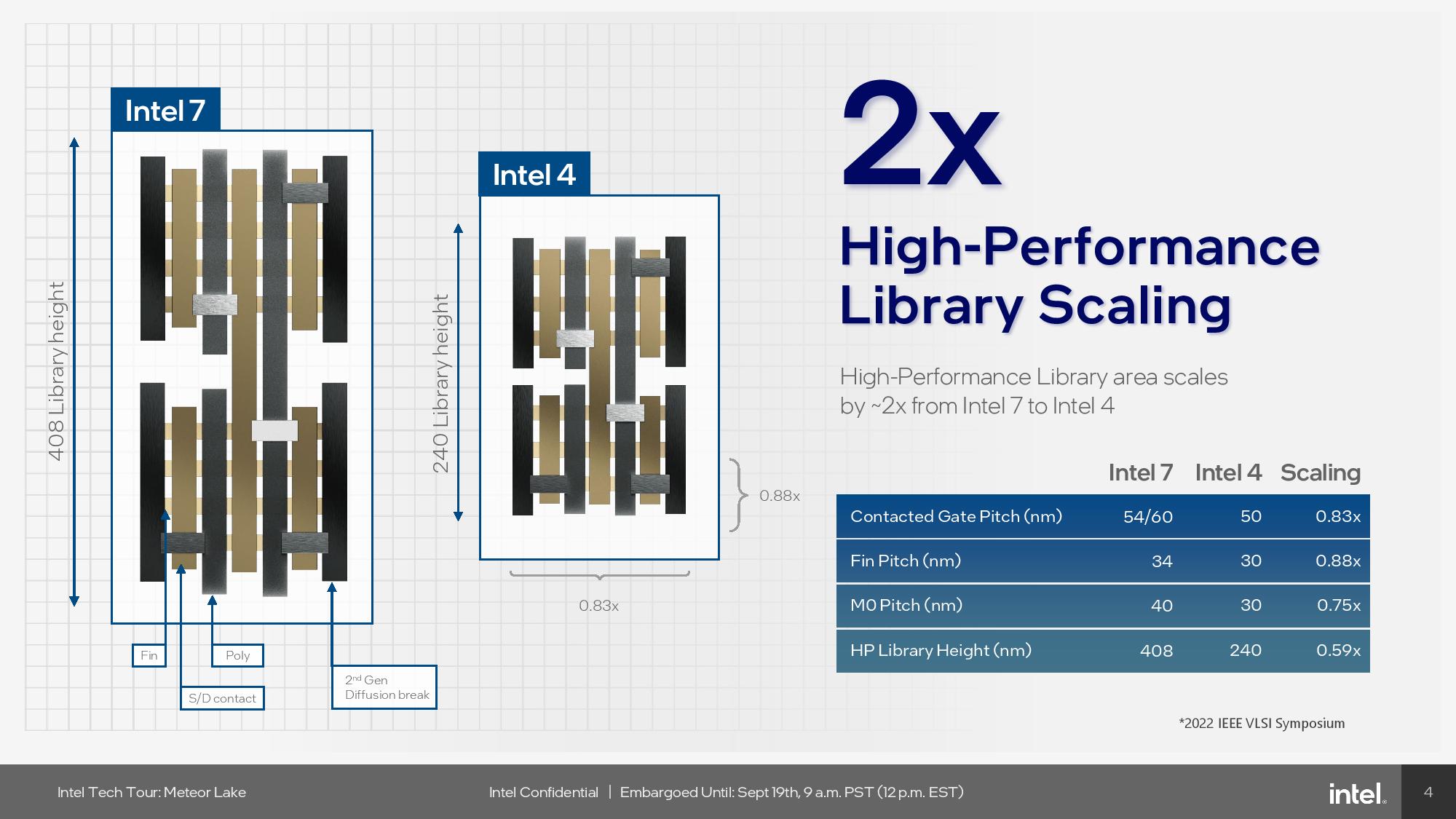
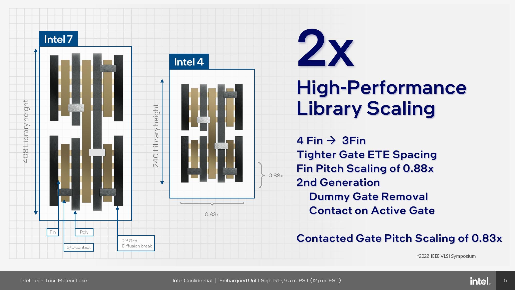
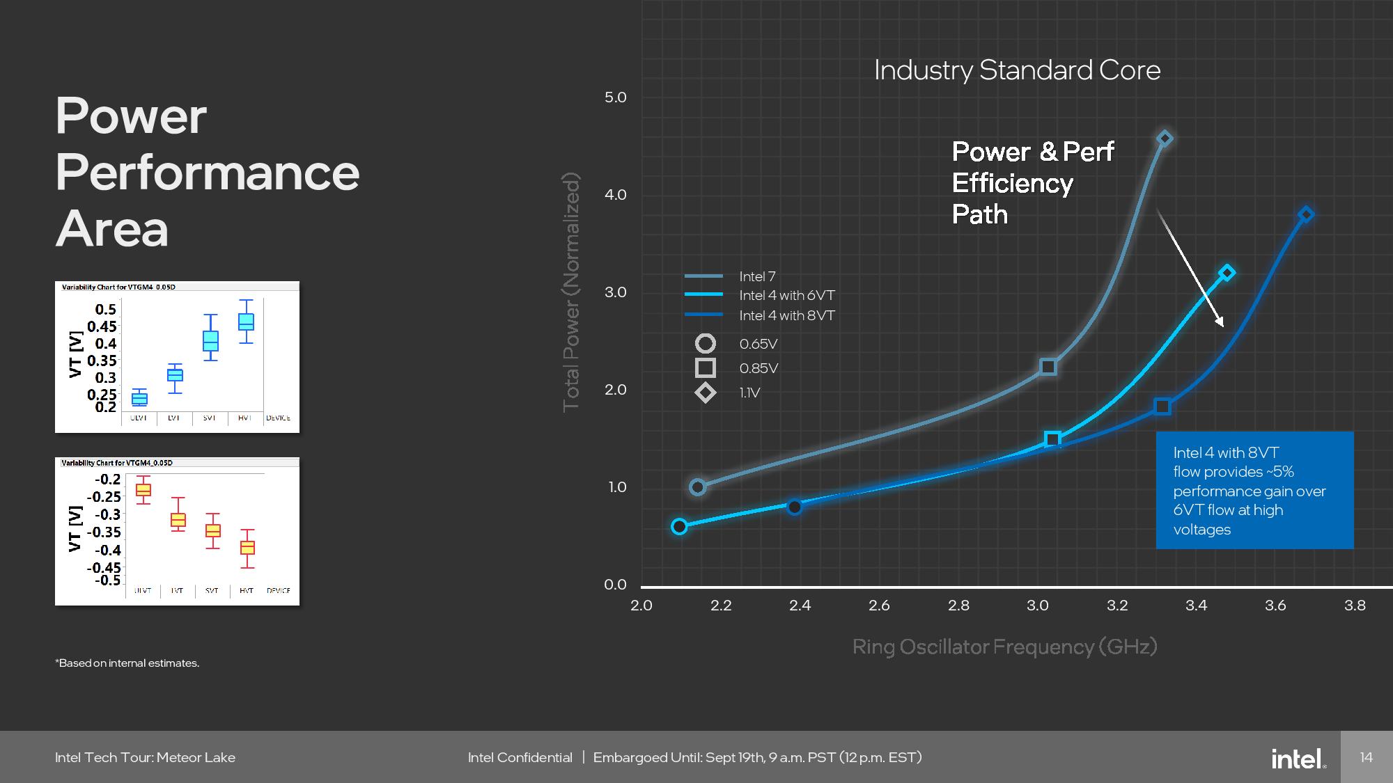
The health of Intel 4, the company’s first node produced with EUV, is exceedingly important as the company looks to recover from years of missteps with its process technology. Highlights include a doubling of high-performance transistor scaling over the last node, and 20% higher clocks at the same power threshold.
Intel chose to focus on power efficiency over performance with this node, squeezing out additional power reductions through fine-grained tuning. Intel also offers 8 Vt levels (threshold voltages), including an ultra-low Vt, an improvement over the 6 Vt they typically offer with the first revision of a new node. These Vt levels provide more tunability for the design process.
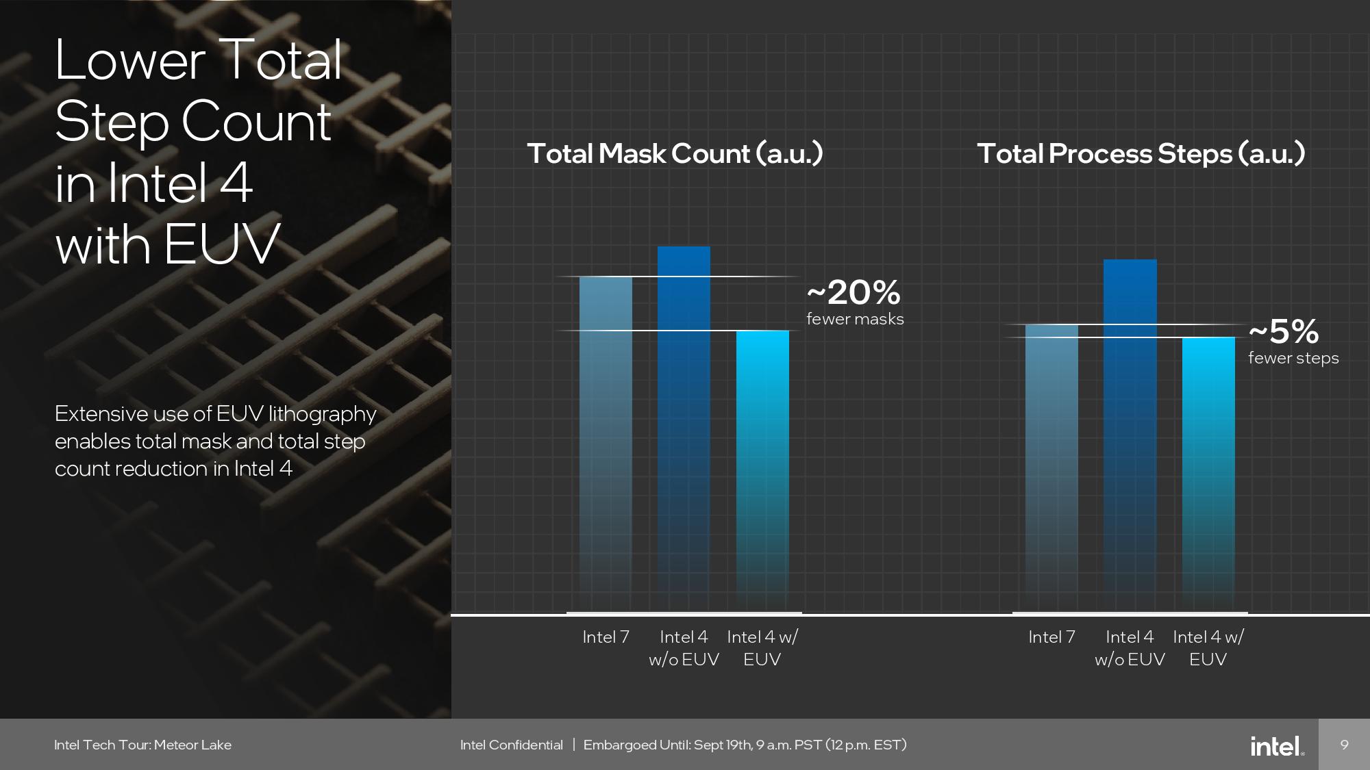
Intel 4 also uses 20% fewer masks and requires 5% fewer processing steps due to the addition of EUV lithography. Intel says this is the first time in the company’s history that the number of masks was actually reduced compared to the prior node.
The slides above give a good overview of the advances Intel has made with Intel 4, but they contain identical information to what we covered when Intel first unveiled the node at its Hot Chips presentation last year. You can read all of the deep-dive details about Intel 4 in our previous Intel 4 coverage.
Meteor Lake Assembly
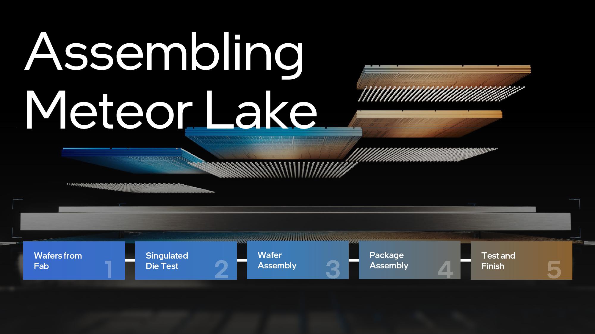
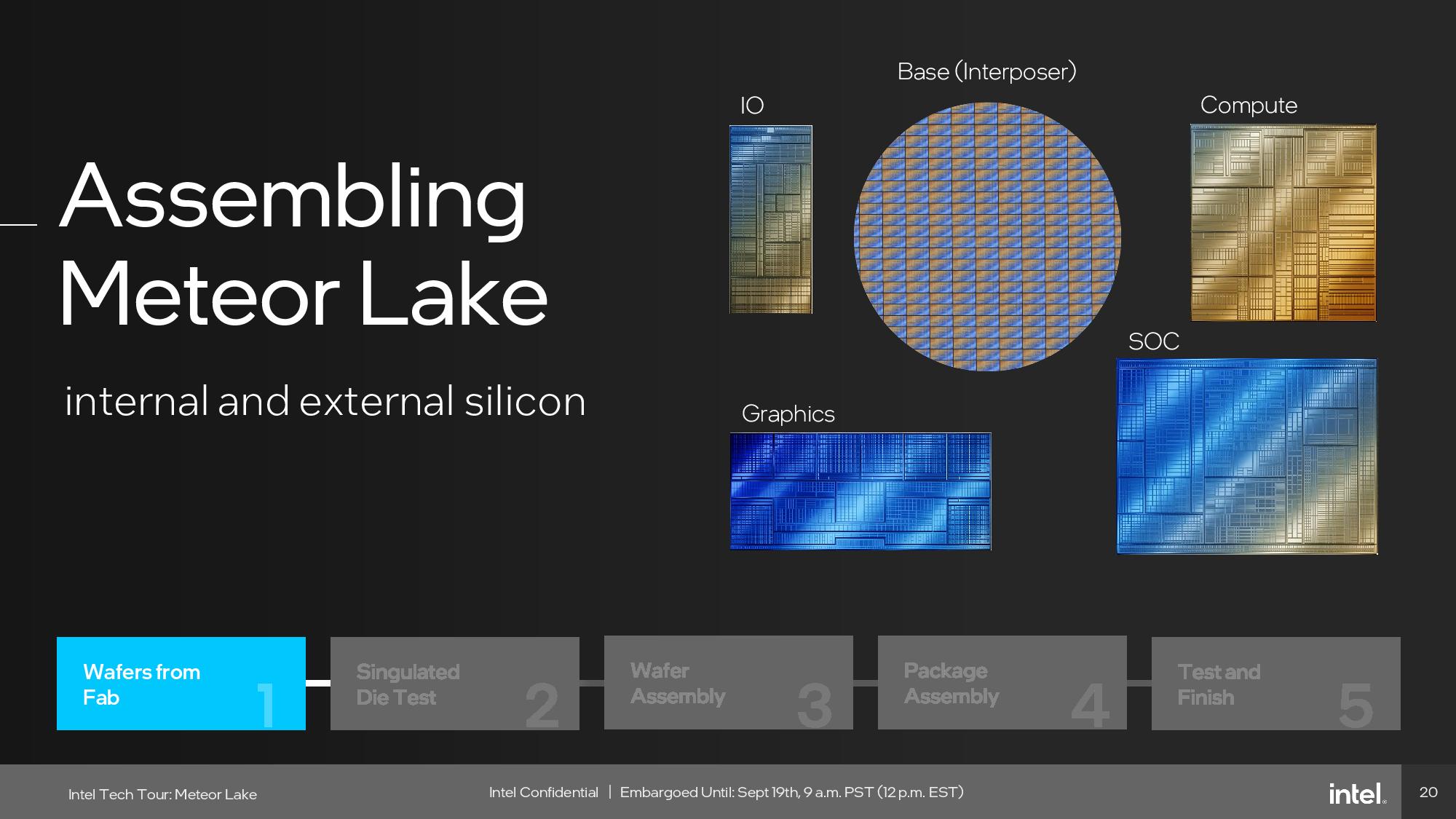
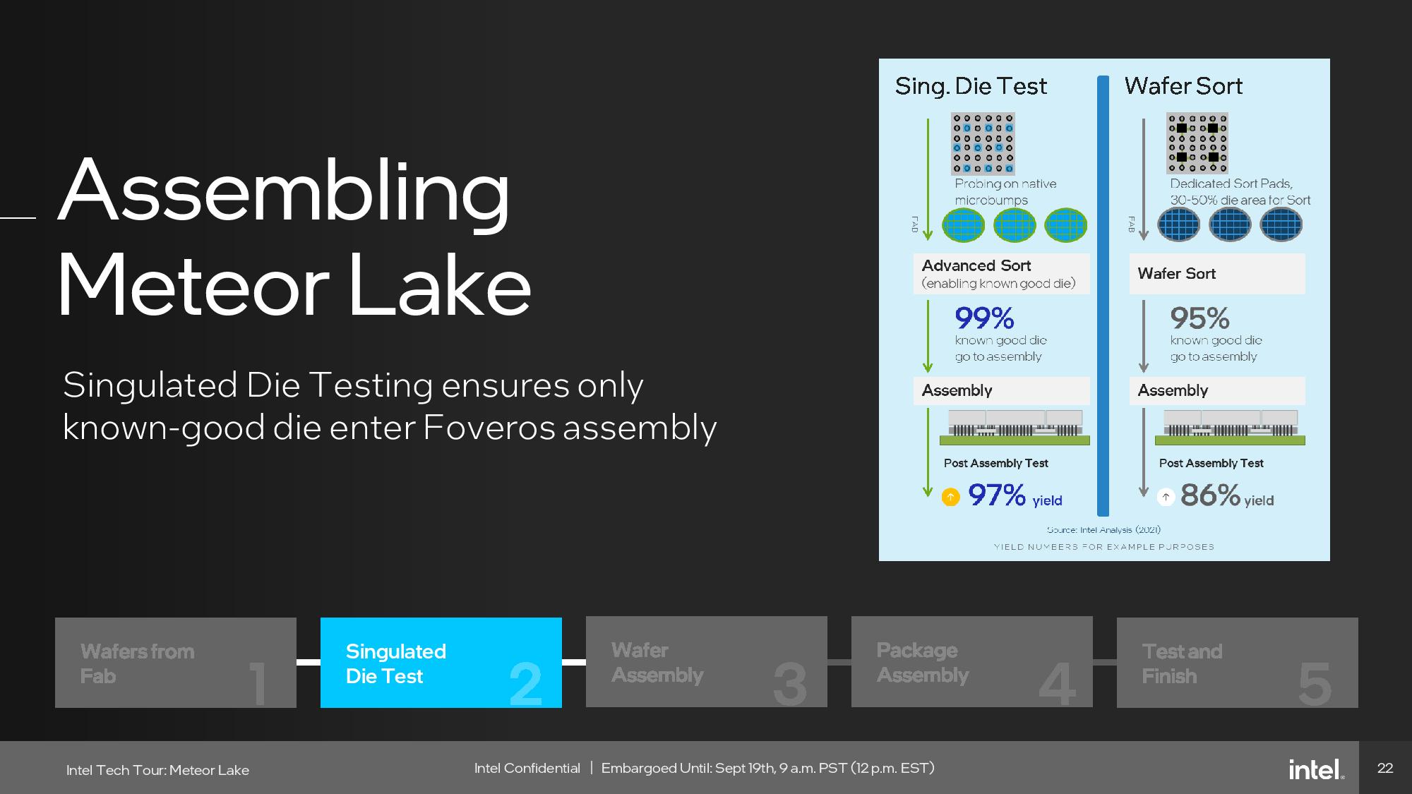
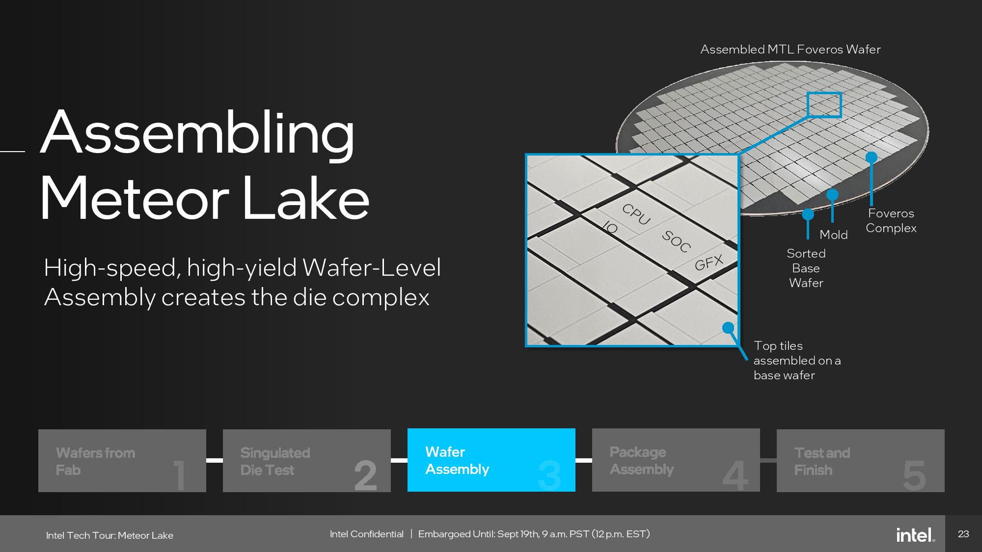
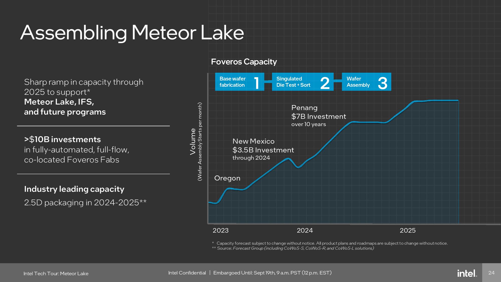
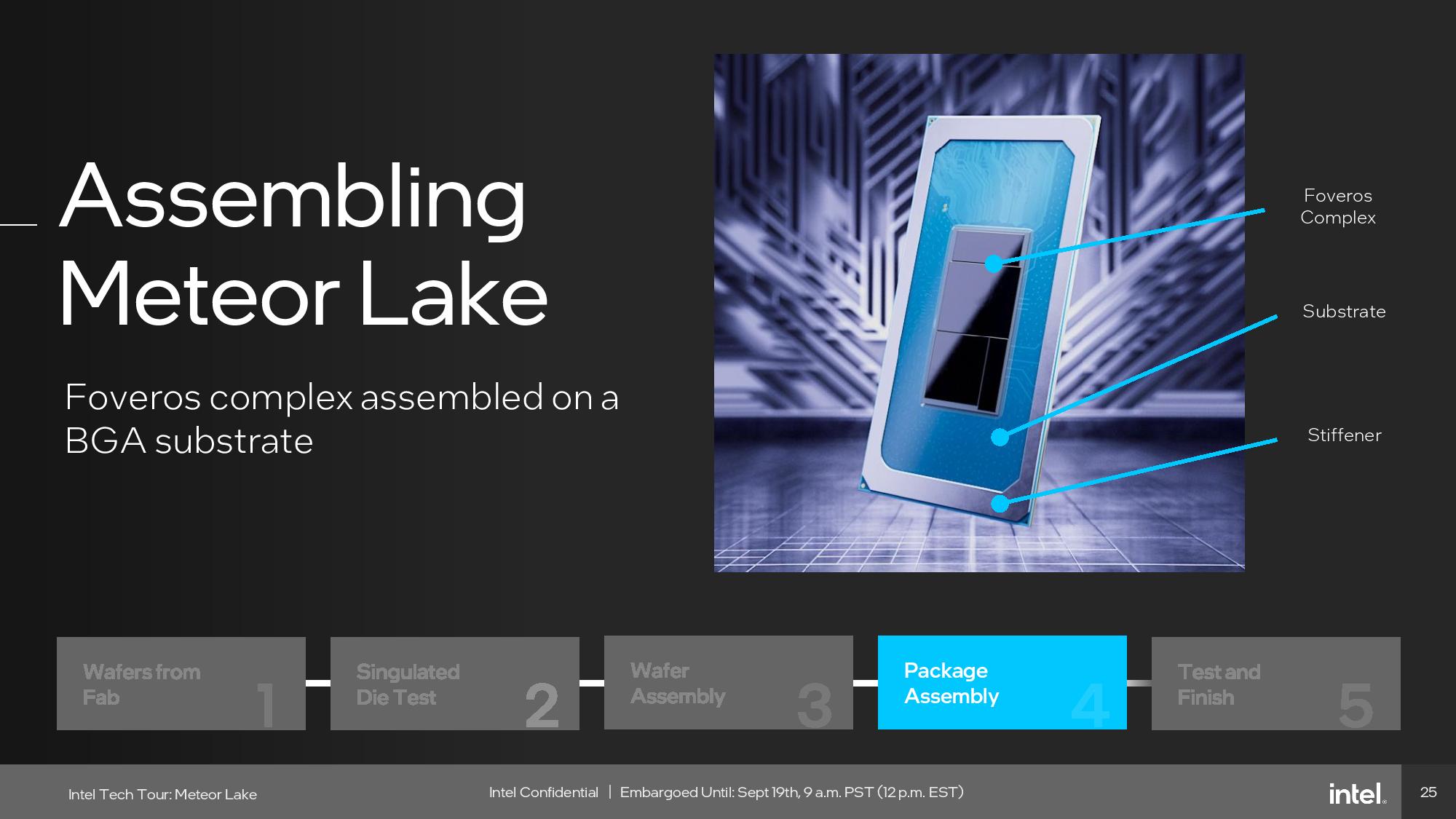
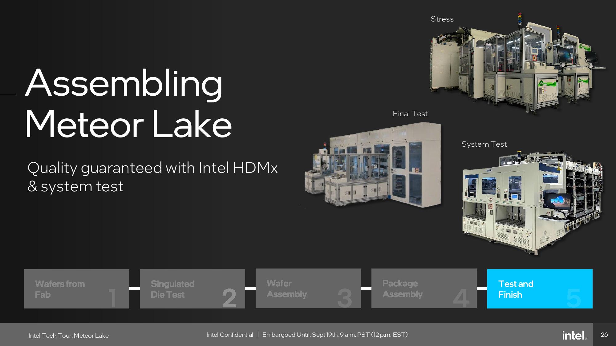
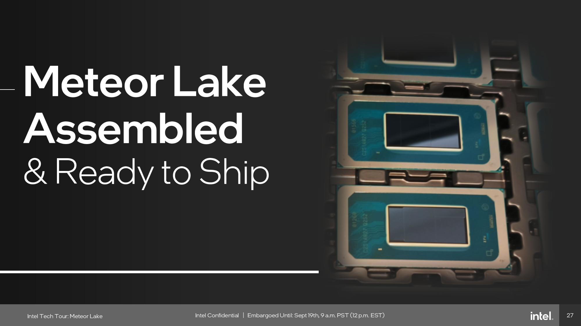
Intel provided an overview of the steps it employs to fabricate a Meteor Lake processor. We also went on a tour of the company’s packaging facilities in Malaysia, and covered this very process in-depth in our recent five-page Inside Intel's CPU Packaging Factory: From Wafer to Chip article.
Thread Director

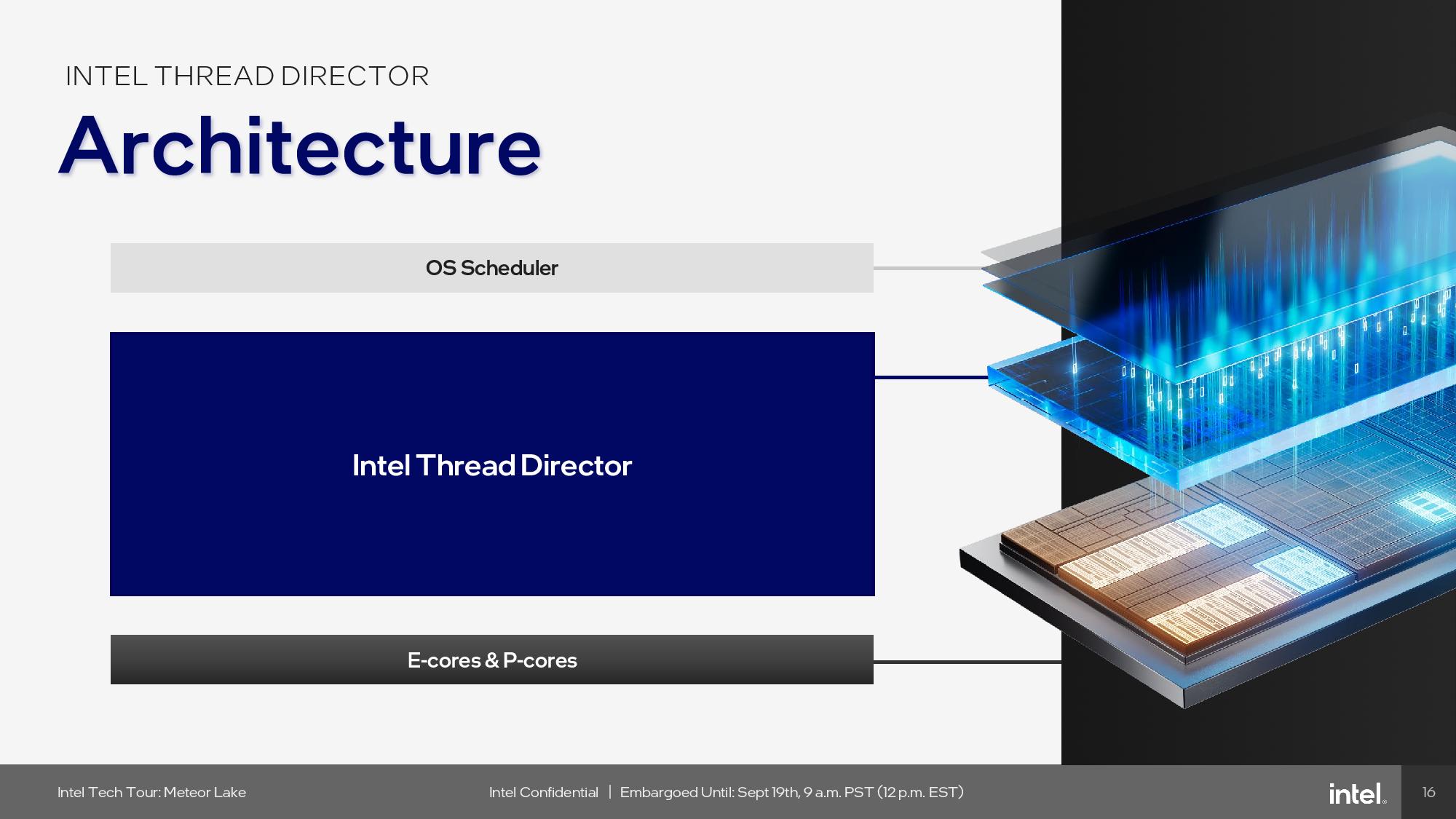
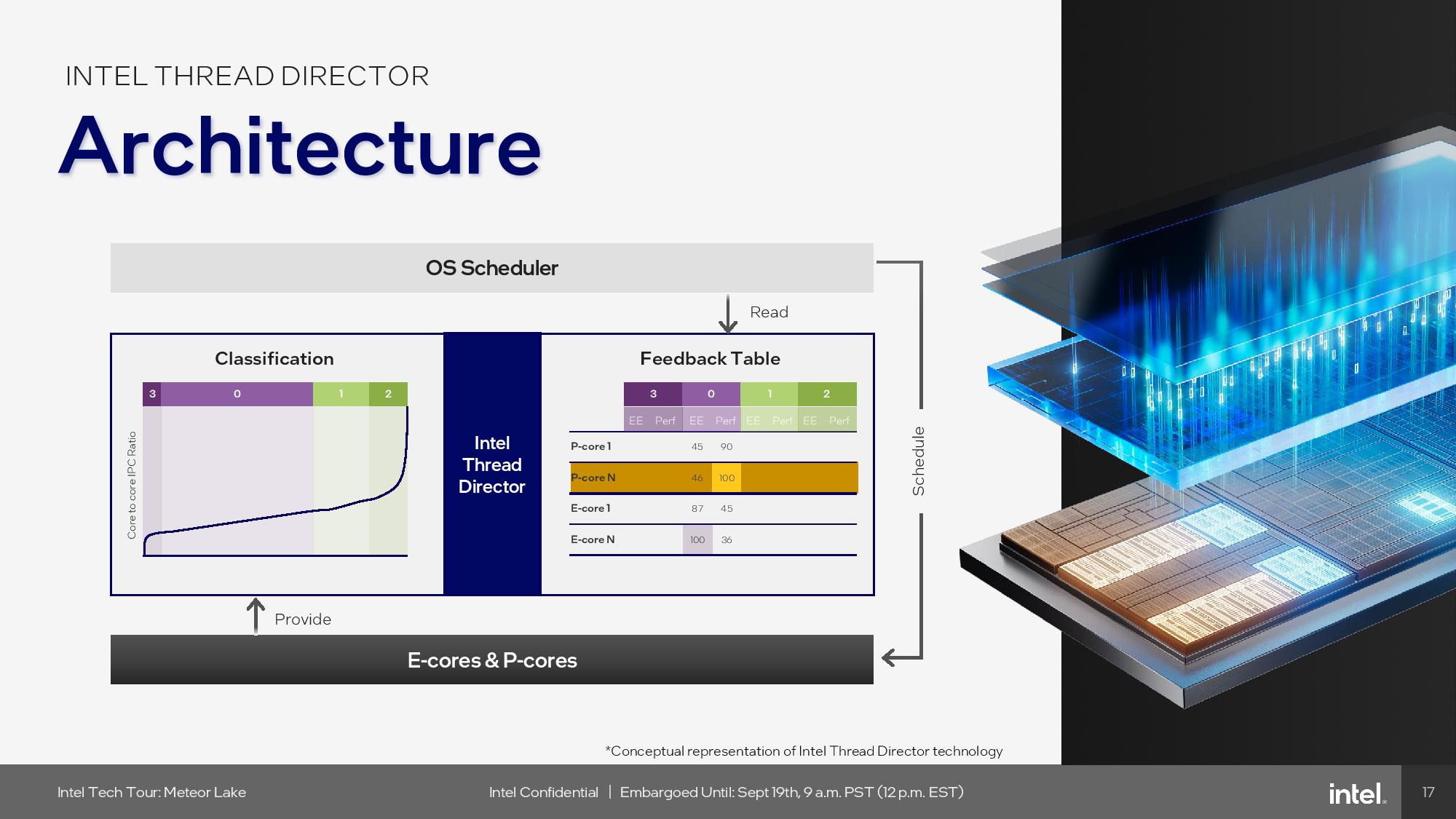
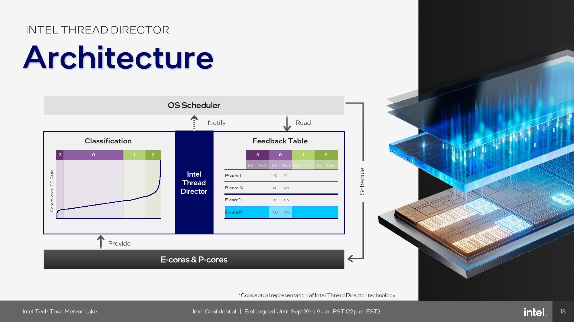
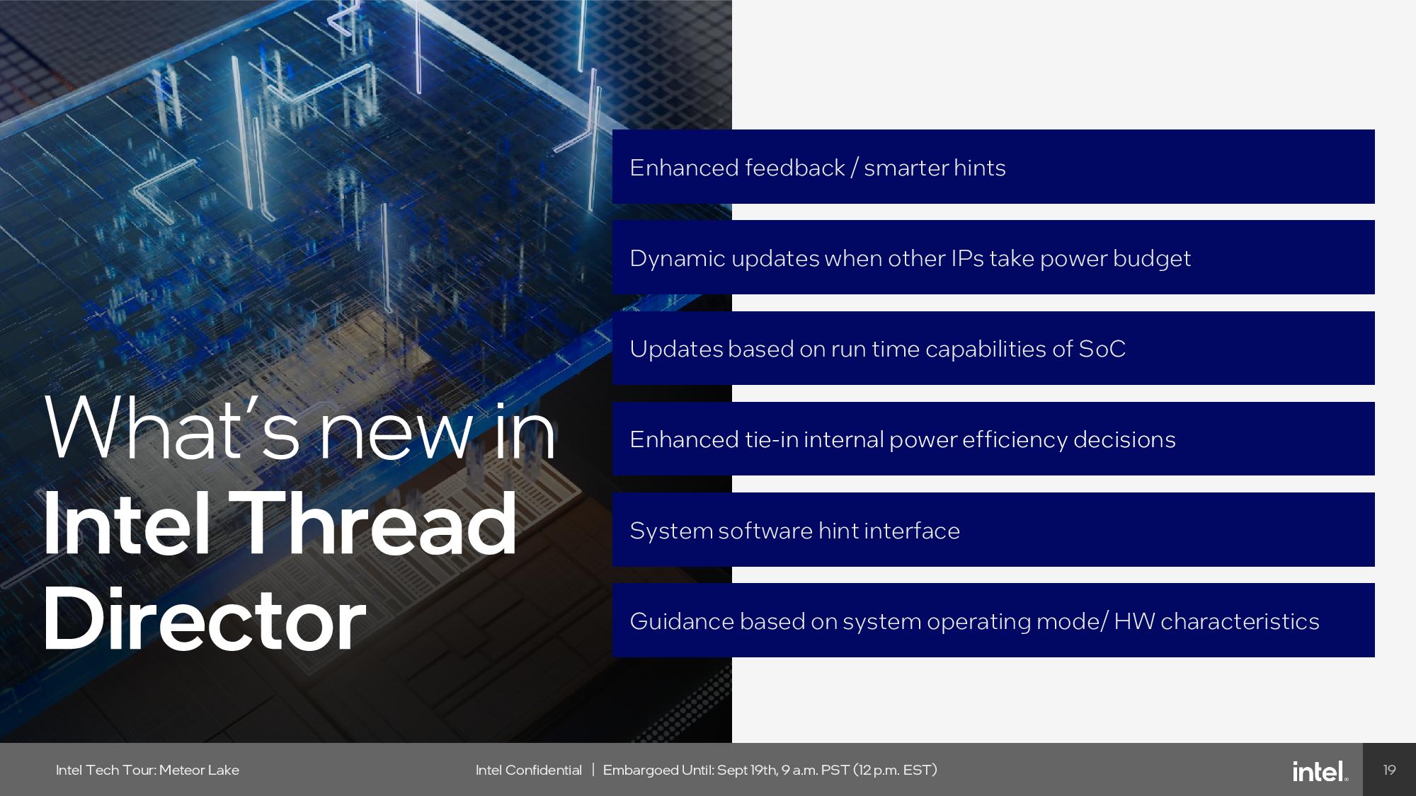

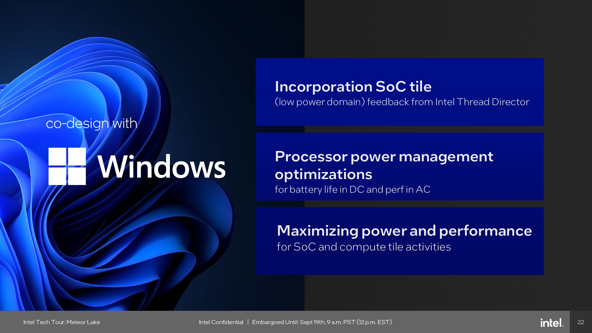
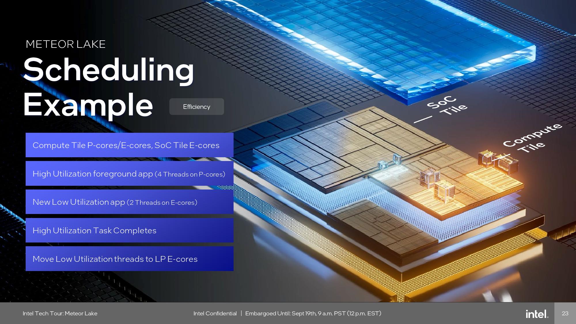
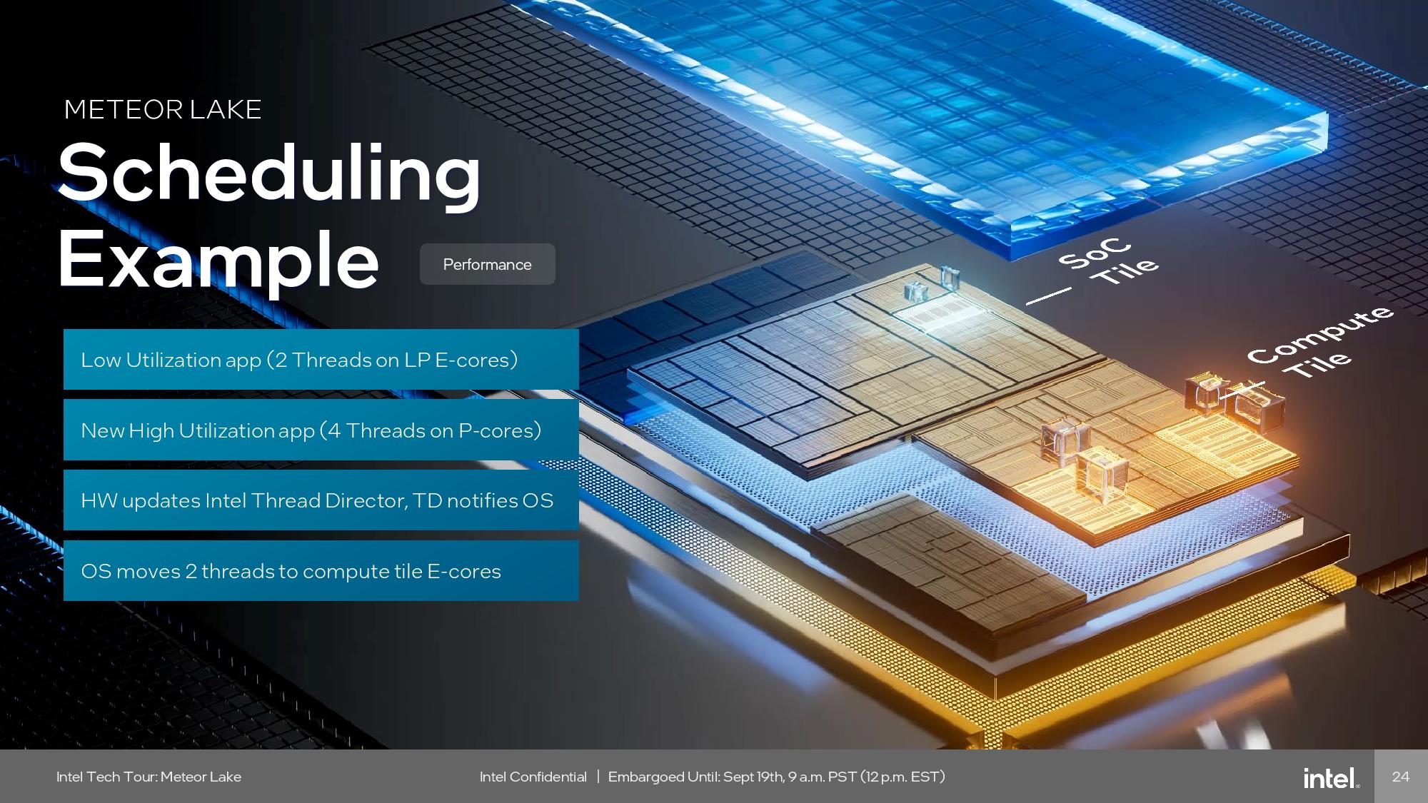
Intel’s Thread Director provides telemetry data to the operating system’s scheduler to help it better steer threads to the correct core, be they P-core, E-core, or the new low-power E-cores. This technology has progressed rapidly since it first debuted with Alder Lake, and the Meteor Lake generation finds Intel once again tuning the engine for its new 3D performance hybrid architecture. Intel expanded the number of rankings in its feedback table to accommodate the new E-cores and tailored the system to provide more information to the OS about the power efficiency of the different types of cores, thus helping it make better decisions. Intel also shifted to a low-power E-core first approach, as outlined in that section of this article.
Thoughts
Intel says its long-awaited Intel 4 process is experiencing better yields than expected, signaling that the company has a solid foundation for building its next-generation Core Ultra ‘Meteor Lake’ processors. The addition of a tiled/chiplet architecture is a watershed moment for the company as it brings its first disaggregated die chip designs to market, all while leveraging externally-sourced chiplets for some key functions to reduce cost and boost performance. With a tremendous re-architecting of the components, augmented by disruptive 3D Foveros packaging technology, and a focus on driving AI workloads, the new Meteor Lake chips do look promising.
Intel has remained coy about performance metrics and SKU details, but it is pounding the drums about its 20% improvement in power efficiency, which could give it a better standing against AMD and Apple’s competing laptop chips that currently lead in those metrics.
As always, the proof is in the shipping silicon. Meteor Lake arrives on December 14, 2023.

Paul Alcorn is the Editor-in-Chief for Tom's Hardware US. He also writes news and reviews on CPUs, storage, and enterprise hardware.
-
evdjj3j The Intel 4 process node has Intel’s highest Day-Zero yields in a decade.Reply
Is that really a high bar considering 10nm? -
TerryLaze Reply
What do you mean?! I am sure they got 10nm to an extremely low loss of yield at some point because it was around for so long but this is about zero-day.evdjj3j said:The Intel 4 process node has Intel’s highest Day-Zero yields in a decade.
Is that really a high bar considering 10nm? -
TJ Hooker Reply
Zero day yields for 10 nm were presumably terrible, given the numerous delays and limited releases. 14 nm also had zero day yield issues, resulting in the delay/limited release of Broadwell. Those are the two nodes Intel has launched in the last decade.TerryLaze said:What do you mean?! I am sure they got 10nm to an extremely low loss of yield at some point because it was around for so long but this is about zero-day.
Their point was that Intel's claim of having the best zero day yields in a decade (with Intel 4) doesn't say much, because that bar is set so low. -
TerryLaze Reply
It has a better initial yield than the refinements of the two previous nodes.TJ Hooker said:Zero day yields for 10 nm were presumably terrible, given the numerous delays and limited releases. 14 nm also had zero day yield issues, resulting in the delay/limited release of Broadwell. Those are the two nodes Intel has launched in the last decade.
Their point was that Intel's claim of having the best zero day yields in a decade (with Intel 4) doesn't say much, because that bar is set so low.
That's still impressive. -
psyconz Reply
Quite surprised to see this interpretation. It seems fairly clear to me that it's comparing zero day to zero day, not zero day to refinements. Am I just blind? ;P TJ Hooker has it correct, as far as I can tell.TerryLaze said:It has a better initial yield than the refinements of the two previous nodes.
That's still impressive. -
spongiemaster Reply
It may not be impressive, but it is important. Intel needs to start consistently delivering on its roadmap. With Intel 4 reaching market this year, it's only a few months late vs their roadmap from 2021, which had Intel 4 products on the market in H1 of 2023. That's world's better than 10nm, and also better than 14nm.TJ Hooker said:Zero day yields for 10 nm were presumably terrible, given the numerous delays and limited releases. 14 nm also had zero day yield issues, resulting in the delay/limited release of Broadwell. Those are the two nodes Intel has launched in the last decade.
Their point was that Intel's claim of having the best zero day yields in a decade (with Intel 4) doesn't say much, because that bar is set so low.
As Terry pointed out, it's also comparing vs the refinements of 14nm and 10nm, so this really is a noteworthy achievement. -
spongiemaster Reply
It's clearly comparing both. There are 2 ticks and 2 tocks on the chart. Tocks are refinements.psyconz said:Quite surprised to see this interpretation. It seems fairly clear to me that it's comparing zero day to zero day, not zero day to refinements. Am I just blind? ;P TJ Hooker has it correct, as far as I can tell. -
TJ Hooker Reply
Ah, I missed that slide. I was just going off the article text, which I interpreted as comparing zero day to zero day yields. Yeah, if Intel 4 yields are already better than mature 14nm and 10nm SF, that is much more impressive.TerryLaze said:It has a better initial yield than the refinements of the two previous nodes.
That's still impressive.
Edit: Well, maybe not "mature", as Skylake was fairly early in the lifespan of 14nm (and potentially a similar story with Tiger Lake, if you consider 10nm ESF/Intel 7 to be a maturation of 10nm SF). But not "zero day". -
JamesJones44 When I read the headline about 2x performance on the iGPU I assumed it would be with the memory on chip vis over chip I/O to the MB.Reply
Looks decent overall, but will have to wait for the benchmarks to get a sense of how much progress Intel has actually made. -
jasonf2 I think the point he was trying to make is that the 4 process node is on track and not going to be another 10nm no show. Refinements or not 10 nm never really made it out of the gate hence 14nm+++++++++++.Reply