Intel's Meteor Lake GPU Doubles Integrated Graphics Performance Per Watt
Arc Alchemist architecture inside
Intel Meteor Lake will come with a significantly upgrade integrated graphics solution. At its Innovation event, Intel provided details on the upcoming Meteor Lake product family, which will arrive later this year. We have a series of articles covering the various aspects of the new architecture, which promises to be a radical departure from prior processors thanks to the use of Foveros chip stacking technologies.
- ▶ Meteor Lake: Core Ultra Architecture Detailed, Due Dec. 14
▶ Meteor Lake GPU: Chip doubles Integrated Graphics Performance Per Watt
▶ 5th-Gen Xeon: Intel Shows 288-Core Processor, Arrives Dec. 14
▶ Arrow Lake Wafer: Showcase for 20A Process Node; Chips in 2024
▶ Pike Creek: World’s First UCIe-Connected Chiplet-Based CPU
▶ Lunar Lake-Based PC: Intel also unveils Panther Lake for 2025
You can find the other articles in the boxout list. We'll be focusing on the display and graphics technologies for this piece. Quite a bit has changed since the previous version of Intel's integrated graphics, Xe-LP. Let's dig into the details of what makes the new Xe-LPG tick, the upgrades from the previous generation GPU, as well as differences between it and the dedicated Arc Alchemist GPUs.
Meteor Lake Graphics Architecture
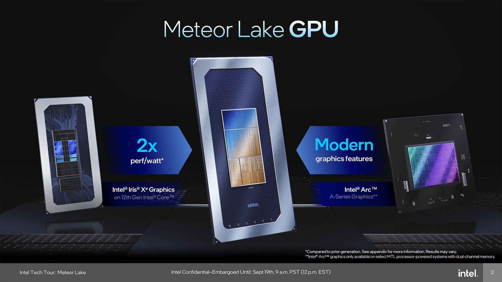
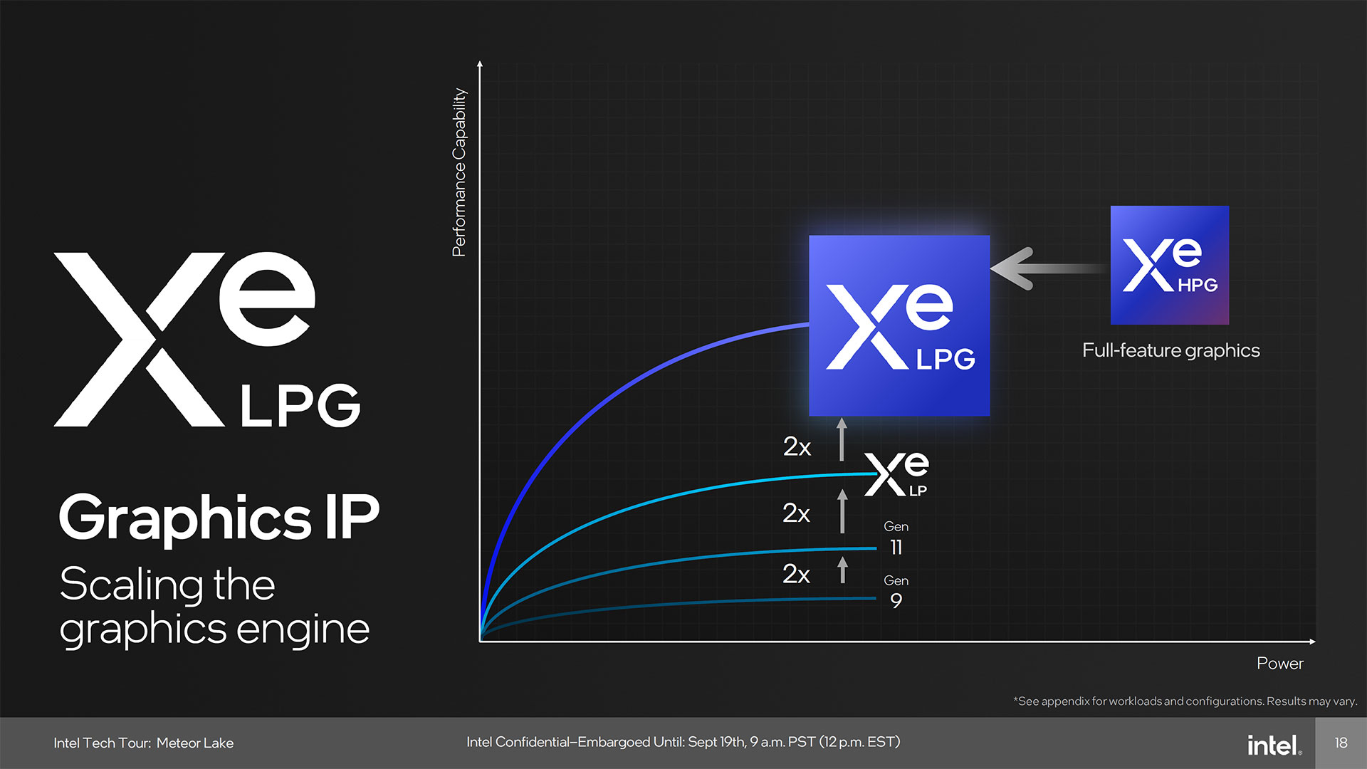
Skipping all of the architectural details for a moment, Intel claims the Meteor Lake GPU will double the performance per watt of its previous generation Iris Xe Graphics solution, which was found in 12th Gen Intel Core processors. While GPUs often lay claim to efficiency improvements, given how power constrained mobile graphics solutions can get, there's a real possibility we could see raw performance double as well. That's a potentially huge gen-over-gen improvement, and there's plenty of other details to dissect.
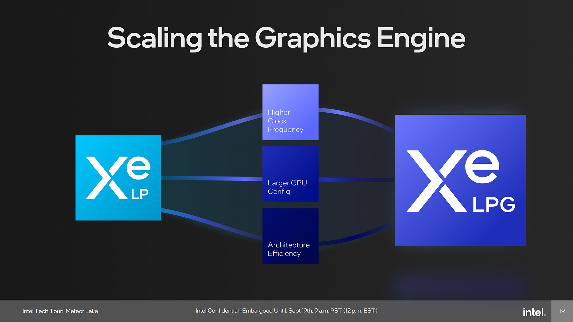
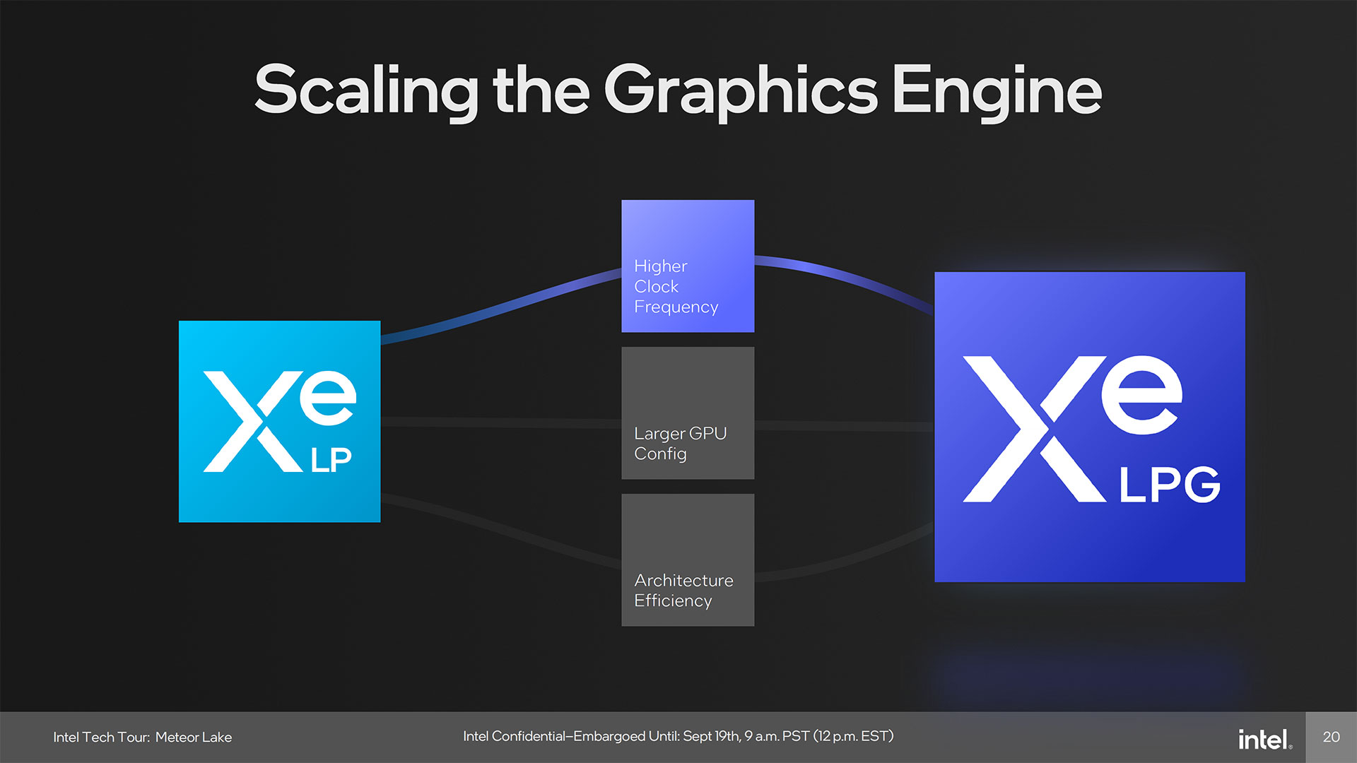
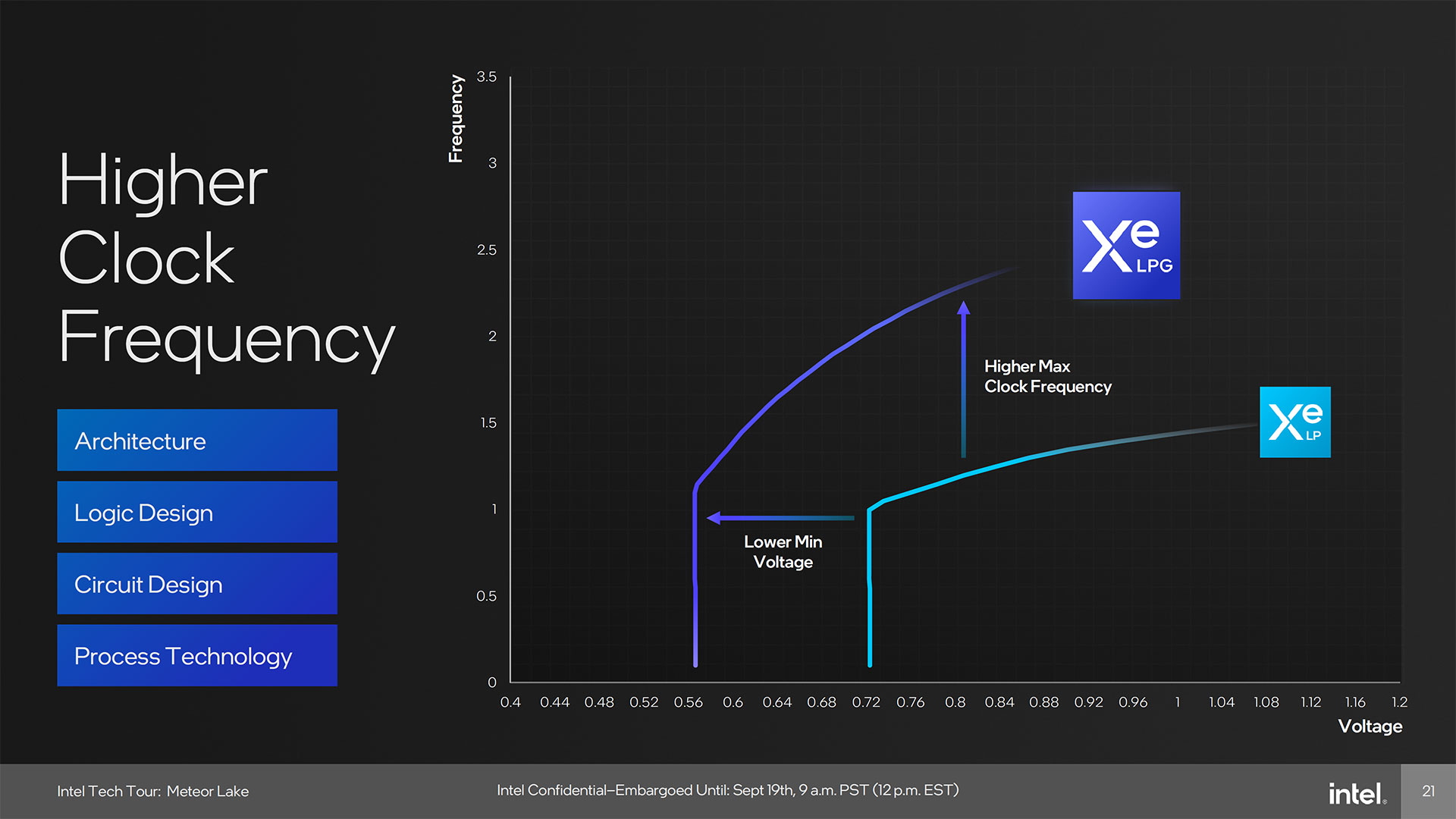
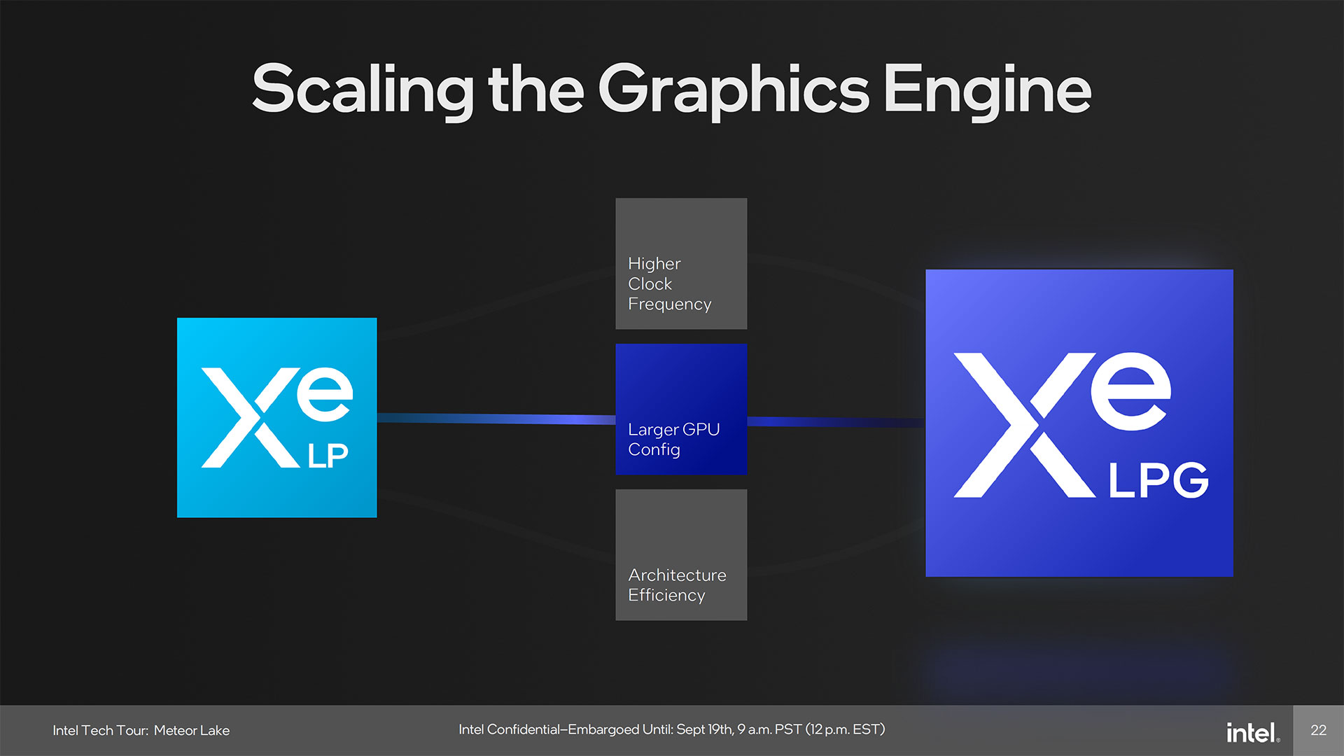
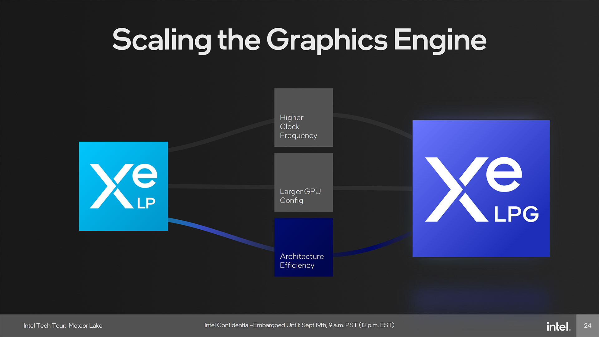
The new graphics architecture is called Xe-LPG, the low power gaming alternative to Xe-HPG — that's the GPU found in the dedicated Intel Arc Alchemist GPUs. It's potentially double the performance of Xe LP, which was the graphics solution used in the 11th Gen Tiger Lake, 12th Gen Alder Lake, and 13th Gen Raptor Lake mobile solutions.
Note also that the highest configurations won't be available on all Meteor Lake processors, though the exact details of the lower tier models haven't been revealed. We'd expect Intel to disable some of the GPU processing clusters and perhaps some of the other extra features on lesser parts, while the Core 5/7/9 chips will offer the complete feature set.
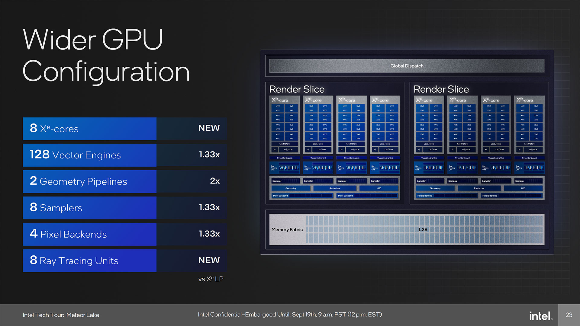
The block diagram for Xe-LPG shows the maximum configuration, which will come with eight Xe-Cores, 128 Vector Engines (formerly called Execution Units), two Geometry Pipelines, eight Samplers, four Pixel Backends, and eight Ray Tracing Units. These will be divided up between the two Render Slices, the main building block for Intel Arc GPUs.
If the above diagram looks familiar on some of the details, that's because it's effectively the same as the ACM-G11 GPU that's used in the Intel Arc A380 — only now it's an integrated graphics solution. Nearly everything present in the A380 appears to be here as well, other than GDDR6 memory controllers and XMX units (more on the latter below). As you'd expect from an integrated solution, the Meteor Lake GPU will share system memory with the CPU.
Intel hasn't provided clock speeds or the L2 cache size yet, but in general we'd expect more conservative clocks than what you'll get from a dedicated A380. That GPU runs at up to 2.4 GHz, but it also consumes up to 75W of power. The mobile Iris Xe meanwhile clocked at up to 1.5 GHz in chips like the Core i9-13905H, with a maximum TDP for the entire package of just 45W.
We could look at this a different way, though, as Intel's Xe DG1 graphics card basically used the same Xe-LP configuration as the integrated chips. It wasn't a very potent solution, and it's little surprise that the Arc A380 easily outclassed the Xe DG1. We expect a similar uplift in performance and capabilities going from integrated Xe-LP to integrated Xe-LPG.
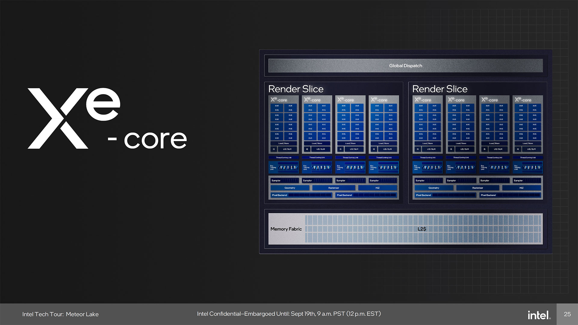
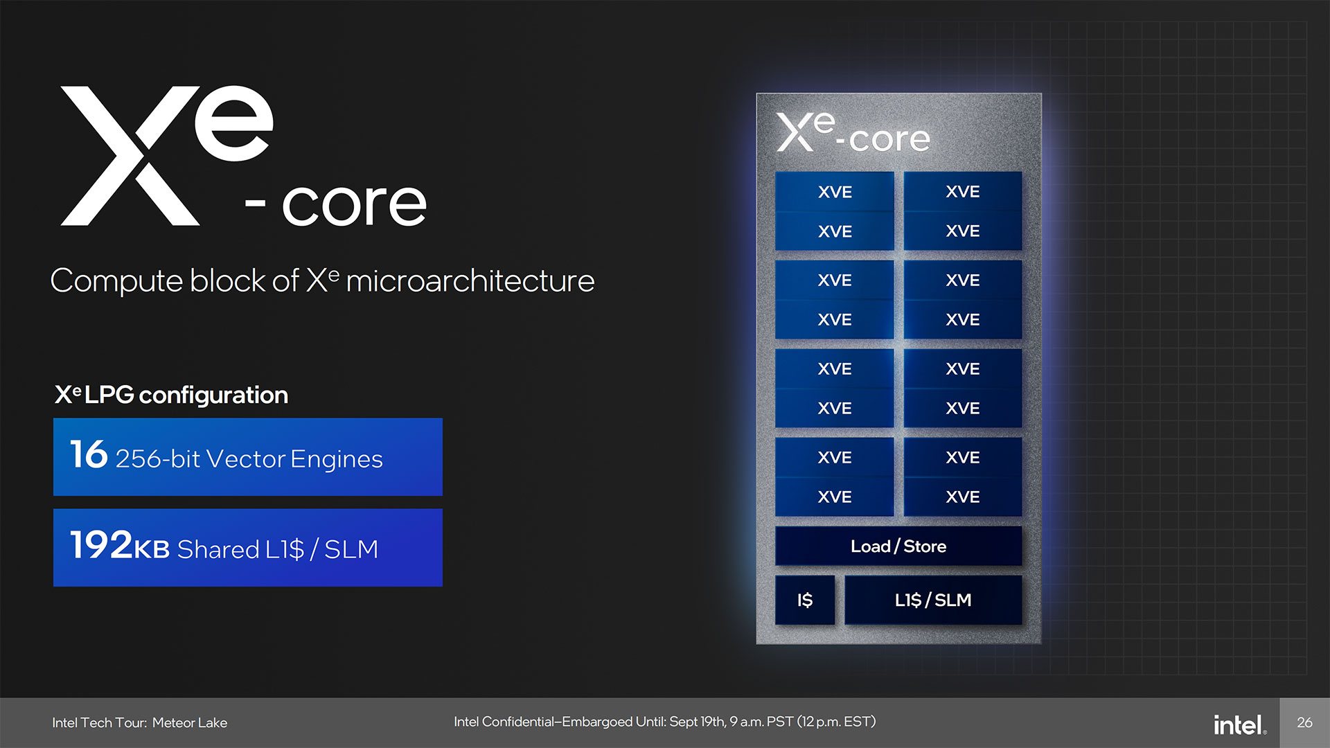
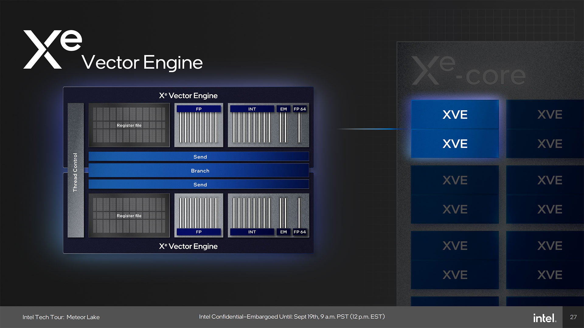
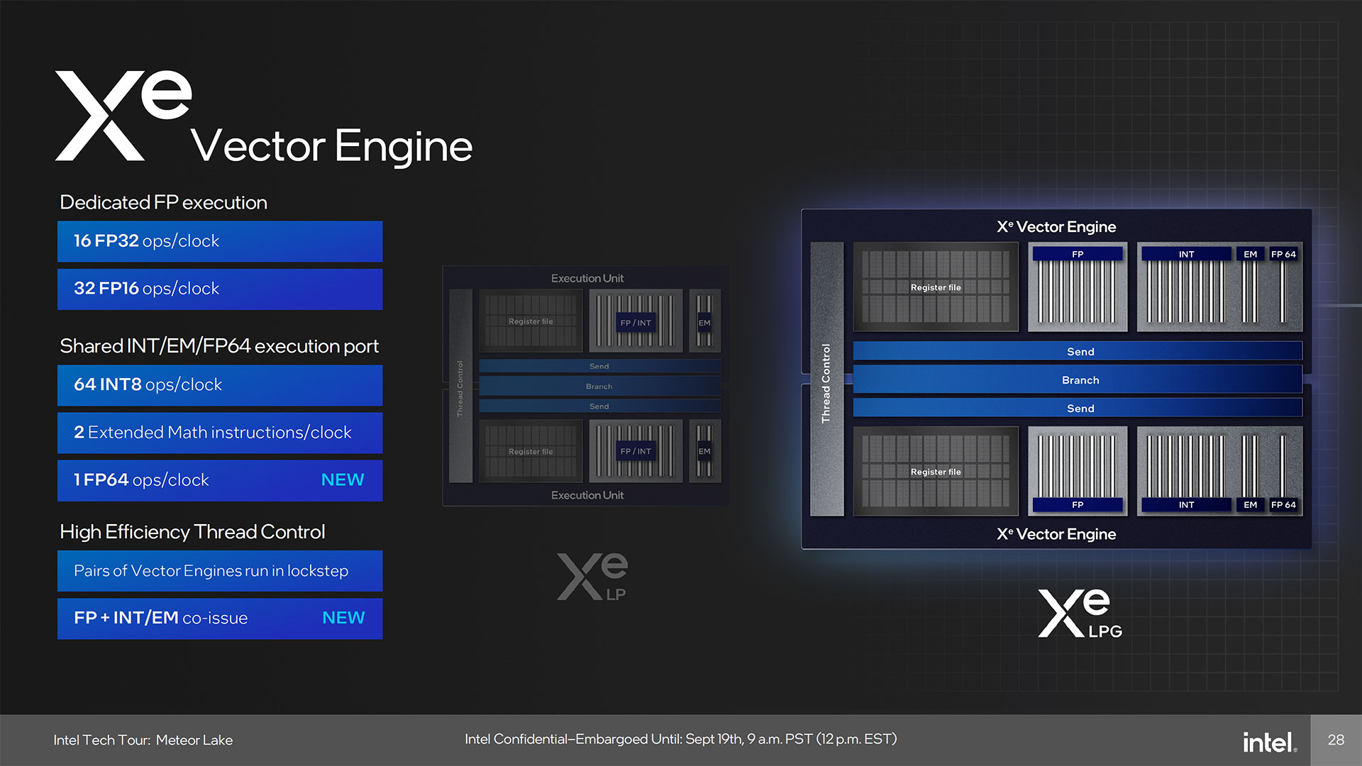
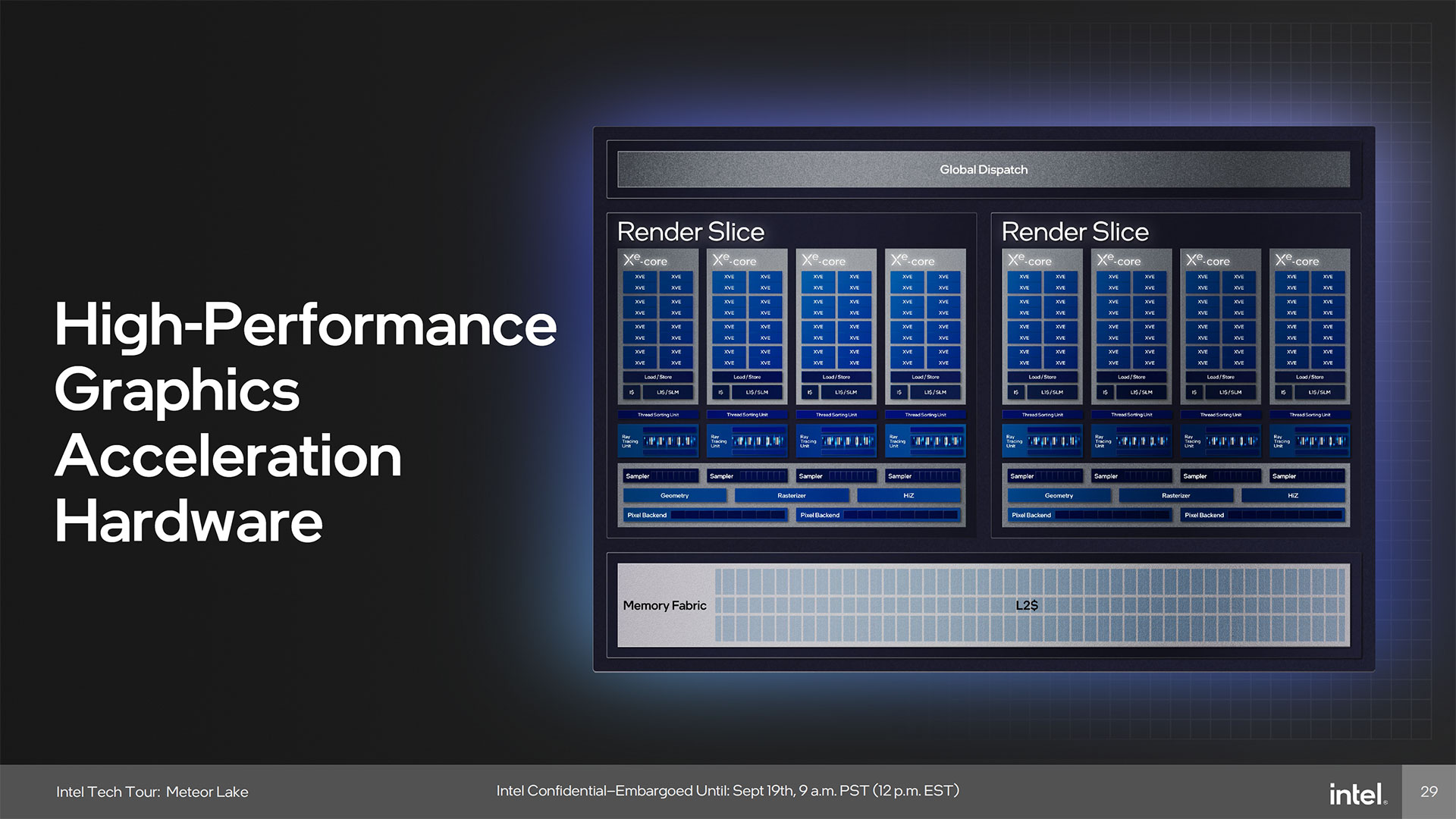
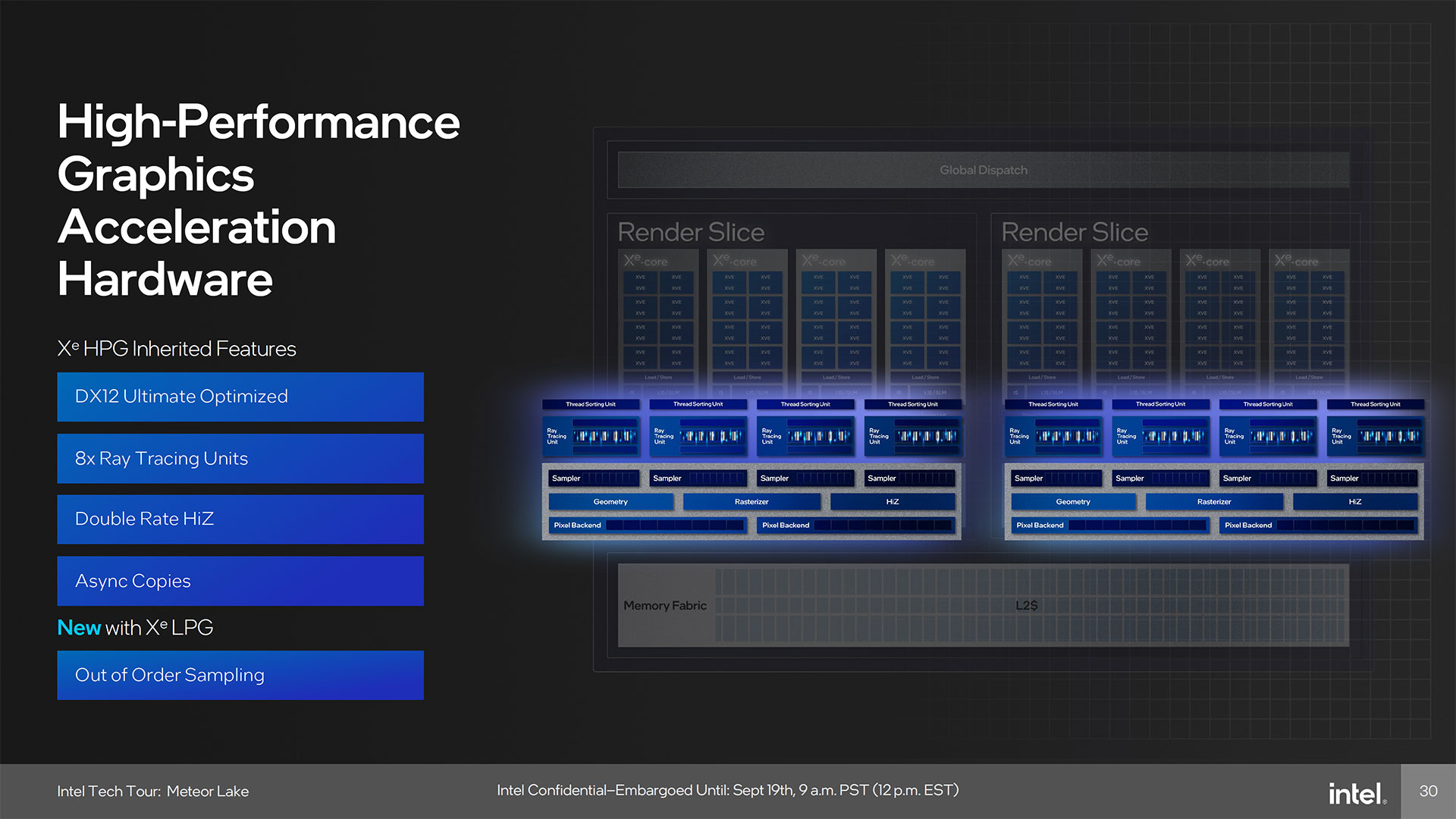
Digging a bit deeper into the graphics hardware, each Xe-Core comes with 16 Vector Engines. Those have the usual assortment of supported number formats, including FP32, FP16, INT8, and FP64 — the 64-bit support is a new feature, incidentally. In total, there are up to 128 Vector Engines in the Meteor Lake GPU, compared to 96 (more limited) Execution Units in the previous integrated GPU.
There's one exception to Xe-LPG basically being like an integrated Arc A380, however: There are no XMX (Xe Matrix eXtensions) units. Those were probably cut in order to help reduce die size, and perhaps power use as well. It's an interesting omission, as XeSS upscaling in our experience looks and performs better on Arc GPUs running in XMX mode compared to XeSS running in DP4a (8-bit INT) mode on GPU shaders.
Intel did double the shader throughput of INT8 operations compared to Iris Xe, however, and each Vector Engine in Meteor Lake's GPU has a rate of 64 INT8 ops per clock. Depending on clock speeds, that's still a fair amount of compute performance: 1.5 GHz (the same as Iris Xe) would be 12 teraops, while 2 GHz (the same as Arc A380) would be 16 teraops. We'll have to see how this plays out in actual XeSS games.
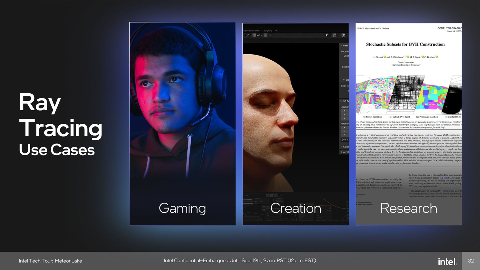
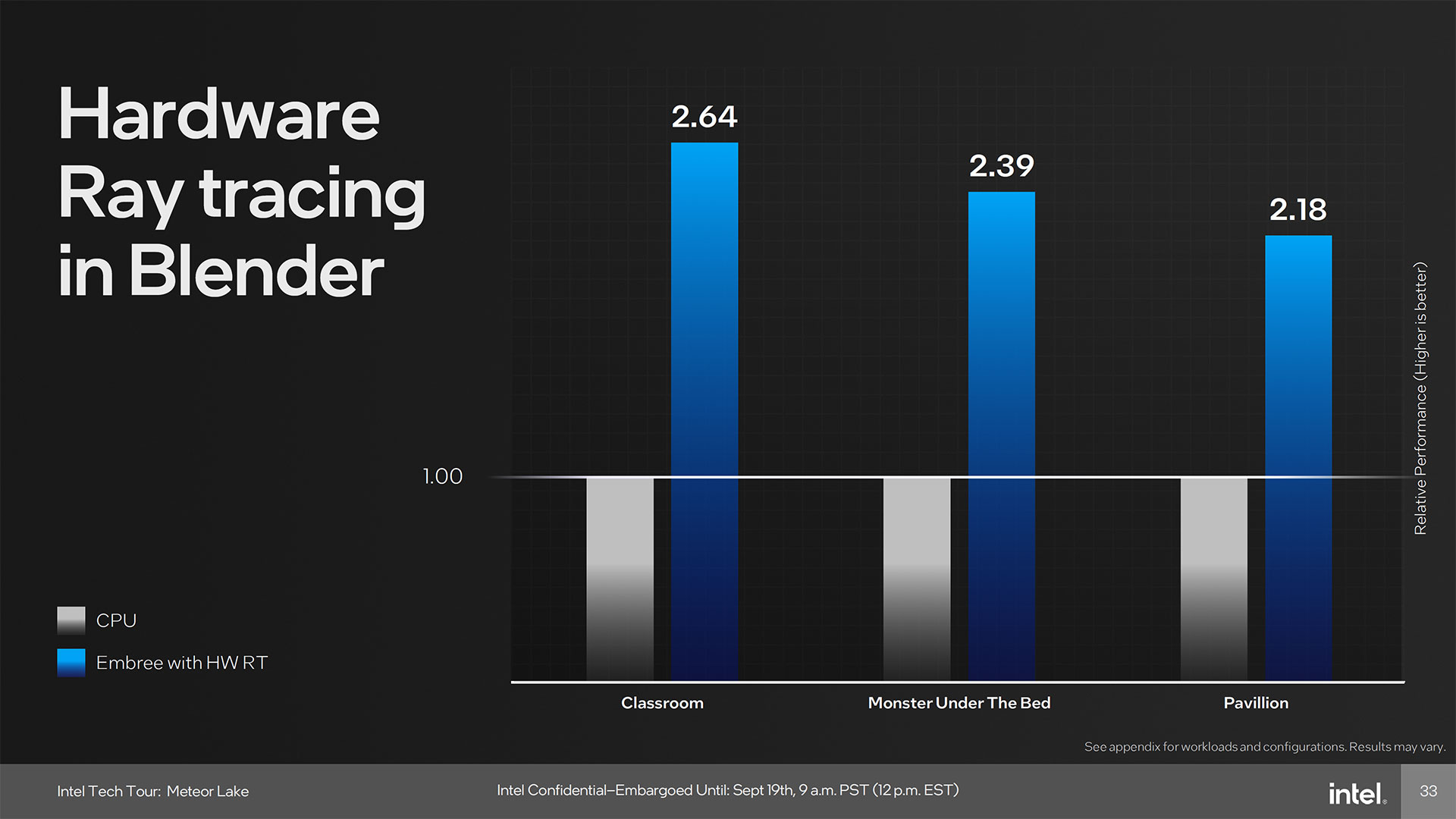
Ray tracing hardware remains, which again represents an interesting set of priorities. The Arc A380 doesn't usually provide a great experience in games with ray tracing, even at lower settings, and having integrated graphics with ray tracing doesn't seem like it would be that important. But Intel notes there are non-gaming use cases for ray tracing as well, for "Creation" and "Research." Blender rendering on integrated graphics shows over 2X the performance of the CPU, according to Intel's slides, but we're definitely not at the point where ray tracing on iGPU is important — or fast enough to matter for most people who do 3D rendering for a living.
Intel also disclosed that the shared L1 cache remains the same 192KB per Xe-core. What we don't know is how much L2 cache will be present. Arc A380 included 4MB of L2 cache. Intel could stick with that amount in Meteor Lake, or potentially even increase the cache size — a larger cache means fewer memory accesses, and the shared system memory may already limit performance a bit.
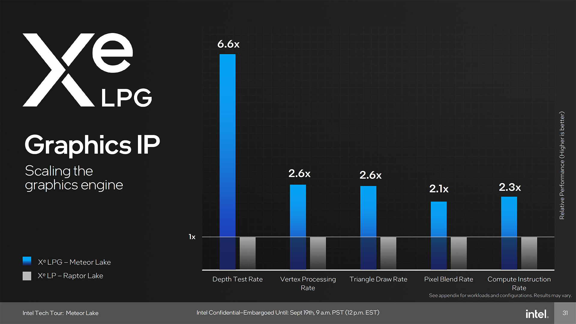
Another slide (number seven in the above gallery) shows the low-level improvements in performance for various graphics related computations, comparing Meteor Lake with Raptor Lake. The Depth Test Rate received a major boost thanks to the double rate HiZ feature. Vertex and triangle processing rates are 2.6x faster, while pixel blend and compute instruction rates are just over 2x faster. Does that equate to double the performance in games? Maybe, but probably not in all cases. We'll have to wait and see.
Meteor Lake Display and Media
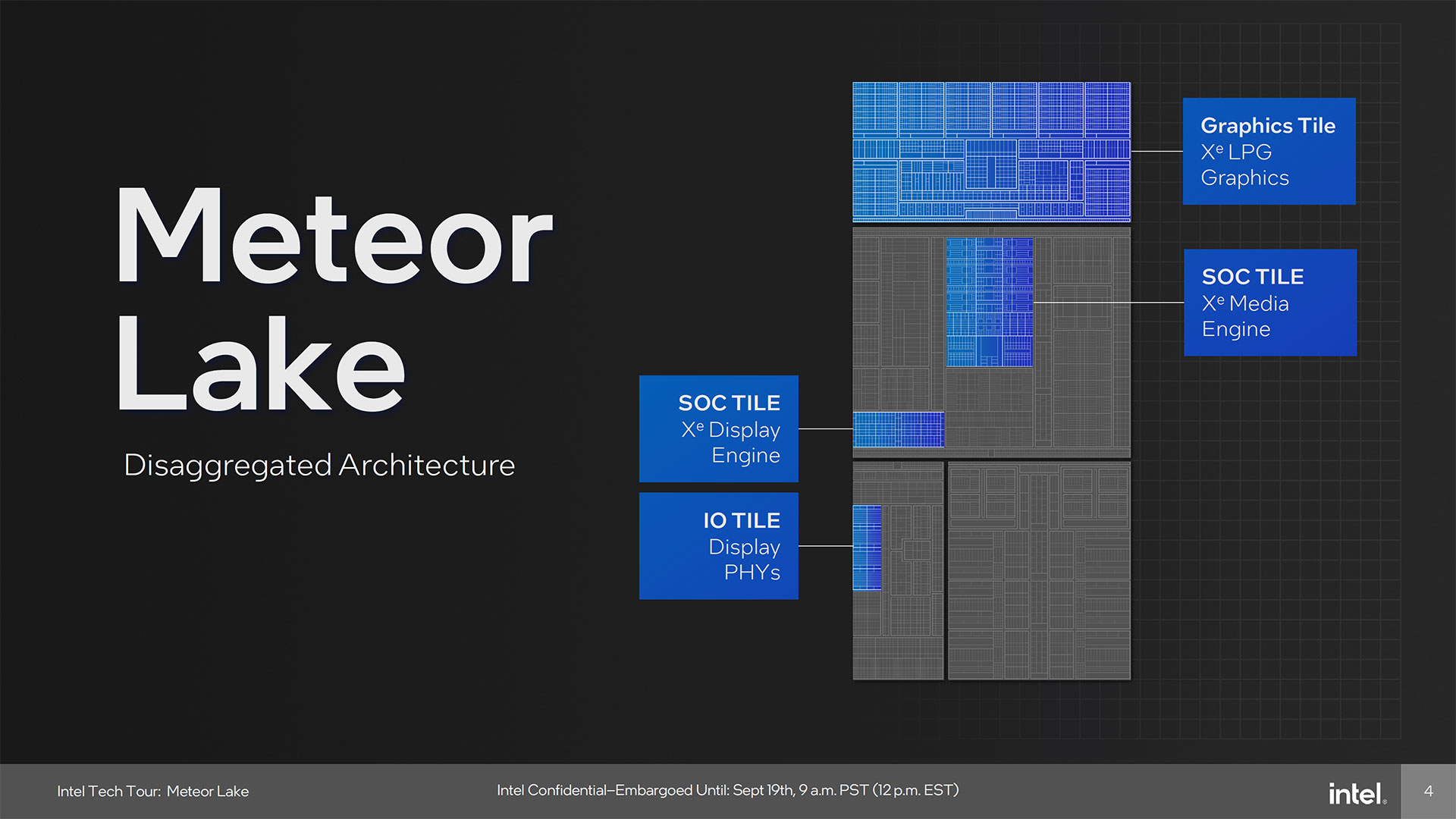
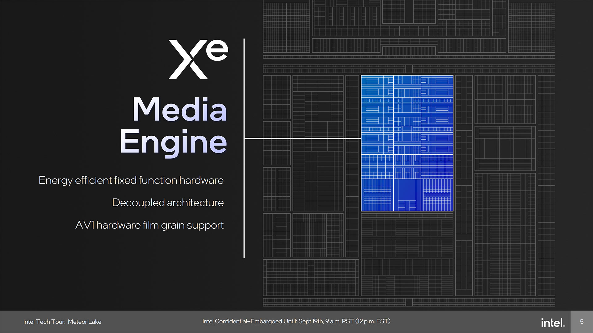
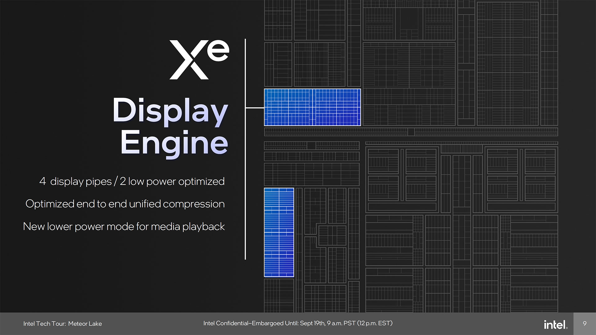
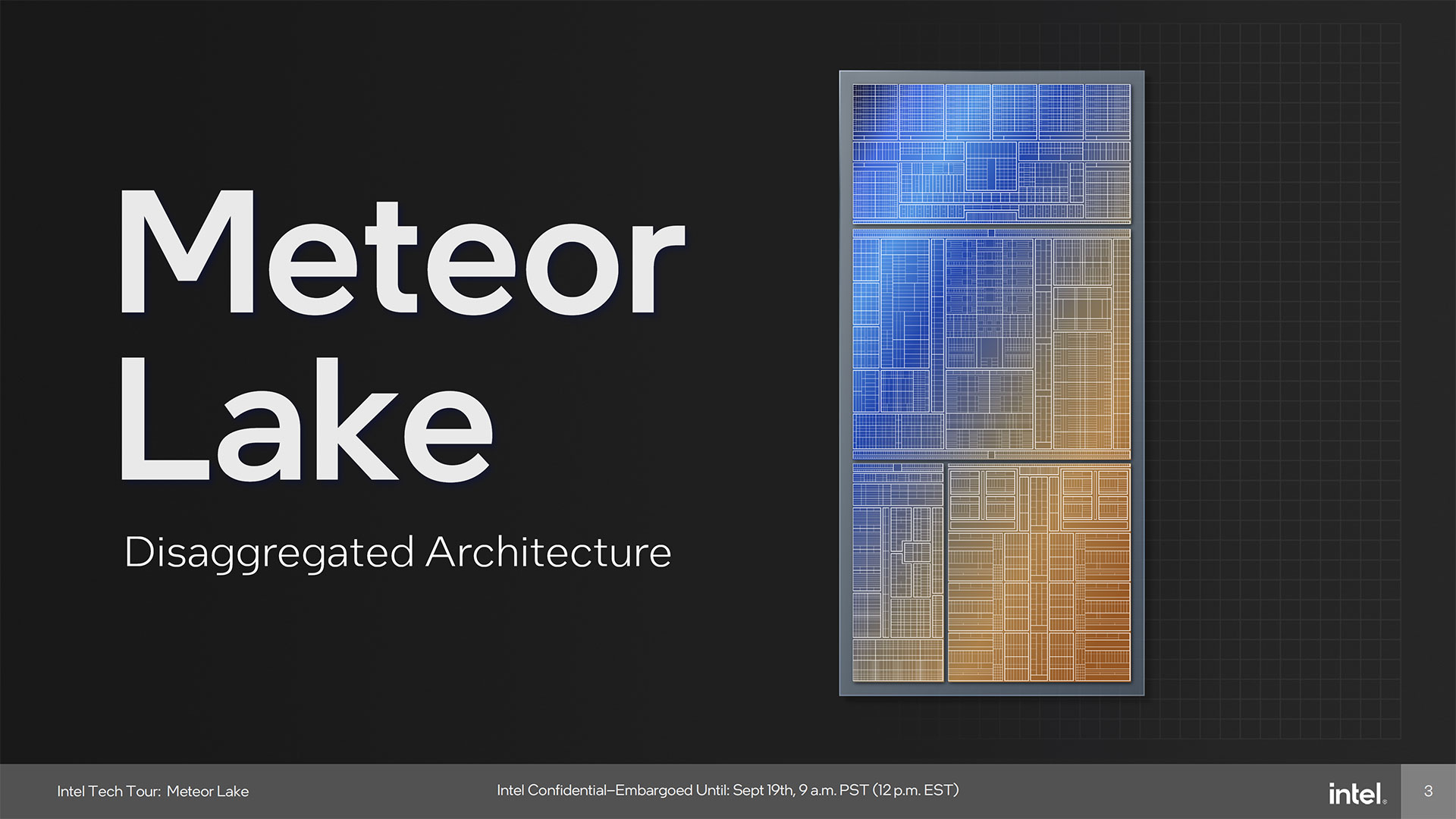
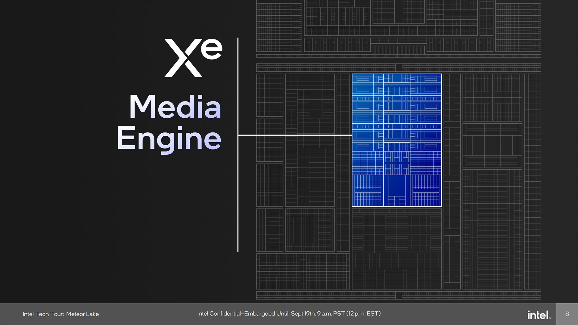
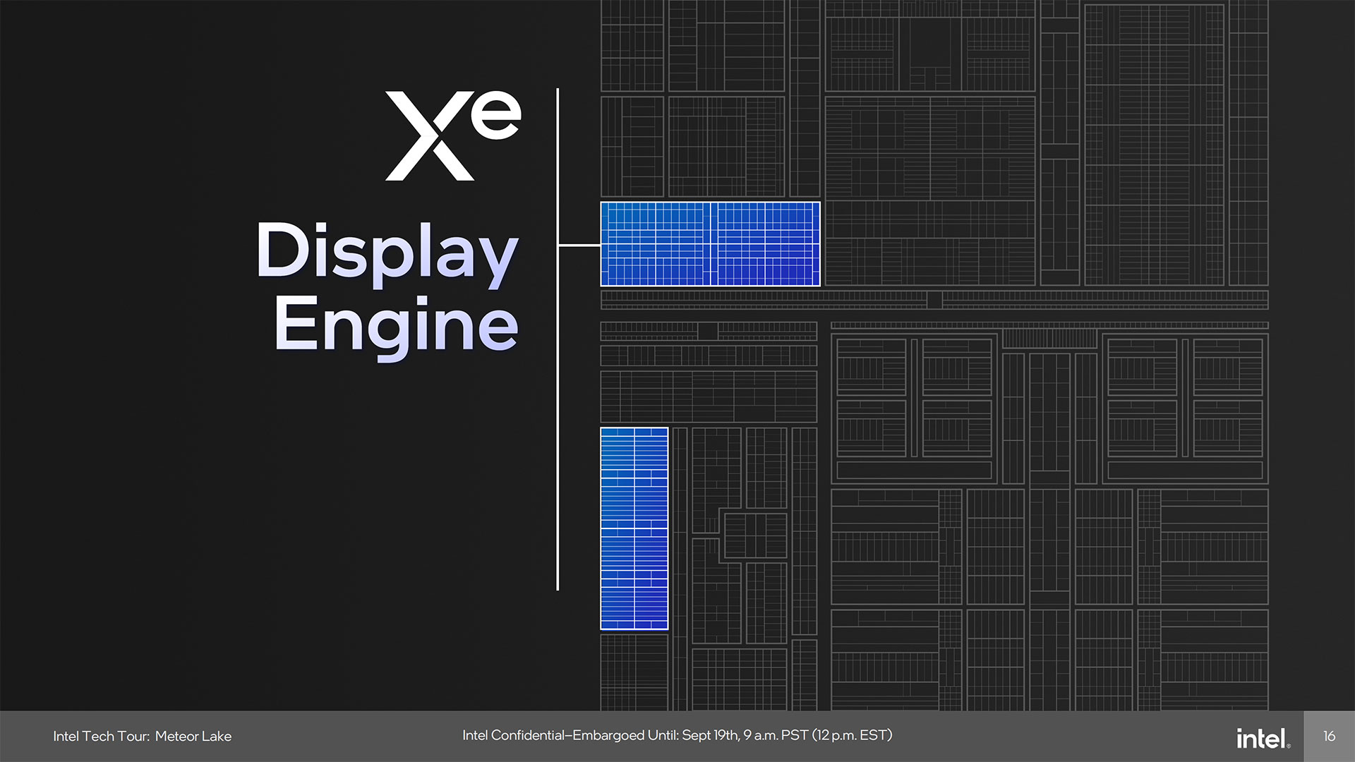
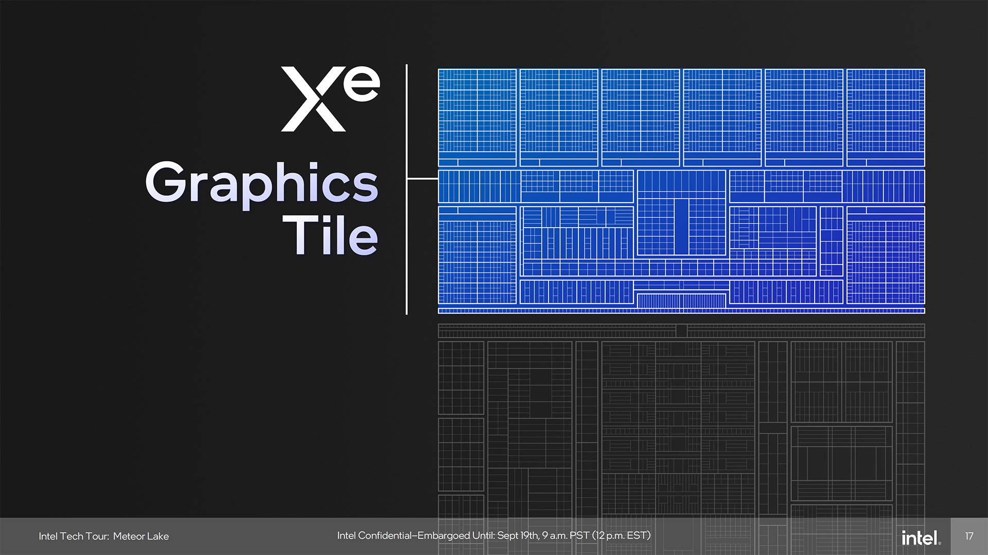
One of the interesting aspects of the Meteor Lake "disaggregated architecture" is how the various elements that would normally be part of the GPU get scattered around the other tiles. The graphics tile handles everything discussed above, while the Display Engine and Xe Media Engine are part of the main SOC tile, and then the physical display outputs are part of the IO tile.
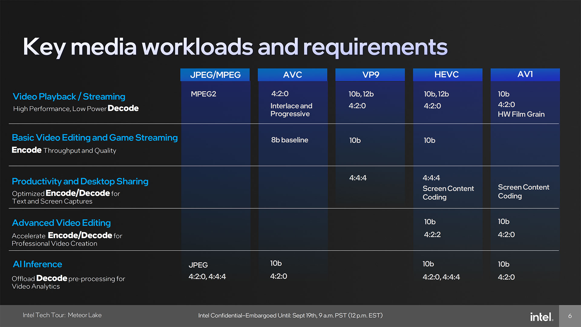
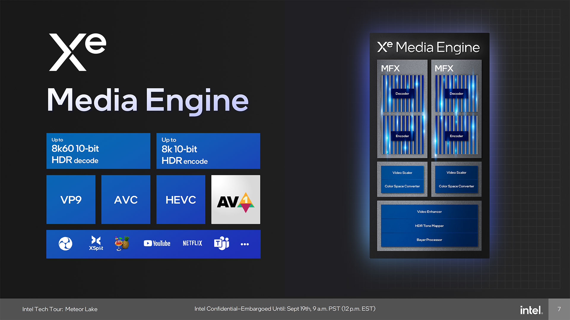
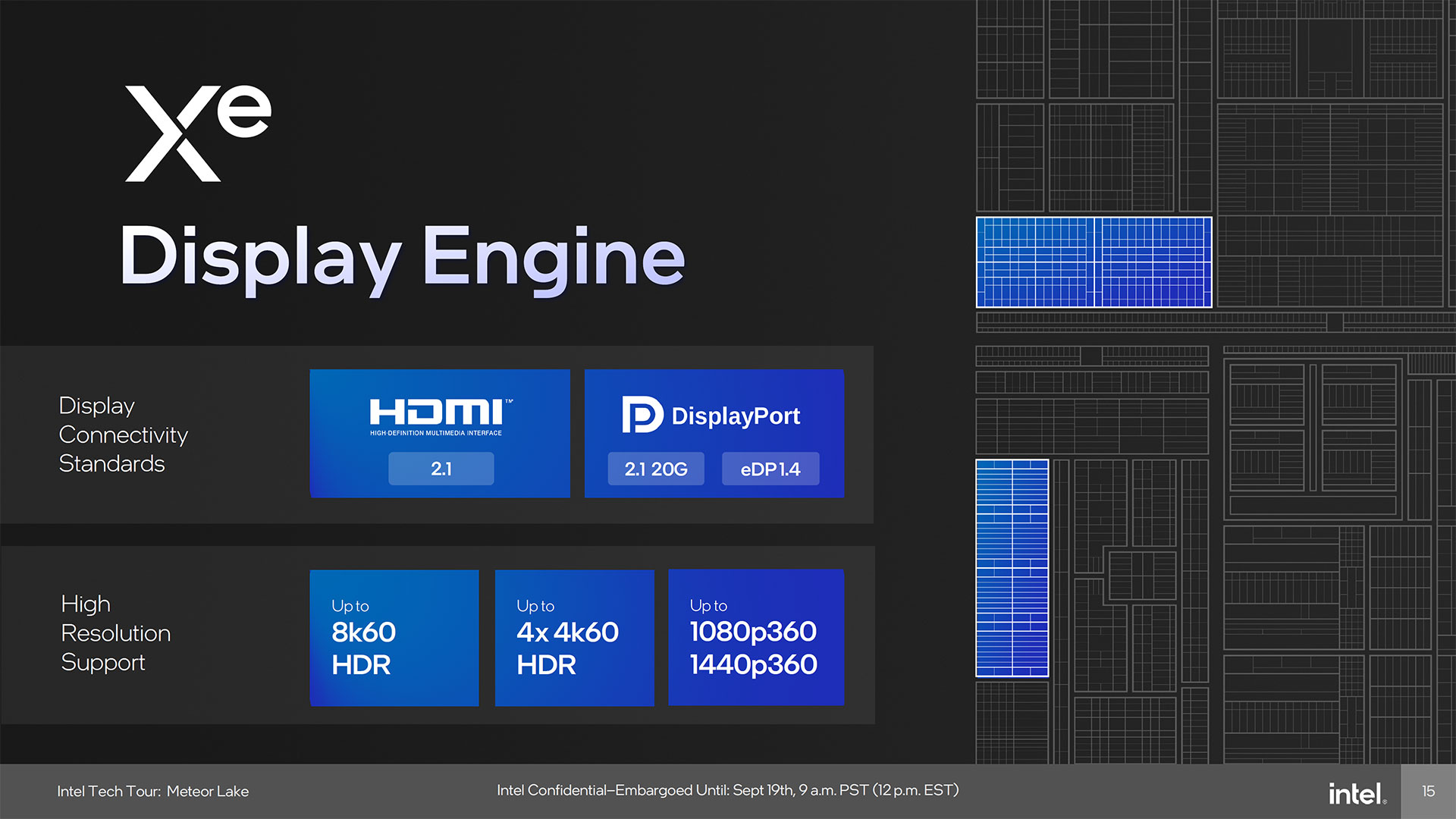
The media capabilities of Meteor Lake are basically the same as Arc. It includes encoding and decoding support for AVC, HEVC, VP9, and AV1 — the latter two being the new additions relative to prior Intel GPUs. It can handle up to 8K60 10-bit HDR decoding, and 8K 10-bit HDR encoding, which should be more than enough for any video streaming tasks.
Putting the display outputs on a different IO tile makes sense, as external interfaces don't scale well at all with newer process nodes. Intel also focused on improving power use on two of the four display pipelines, which should help improve battery life in laptops. There's also a new low power mode for media playback.
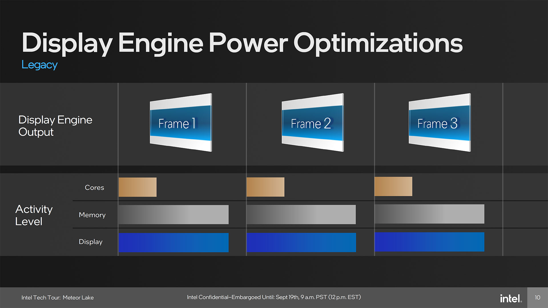
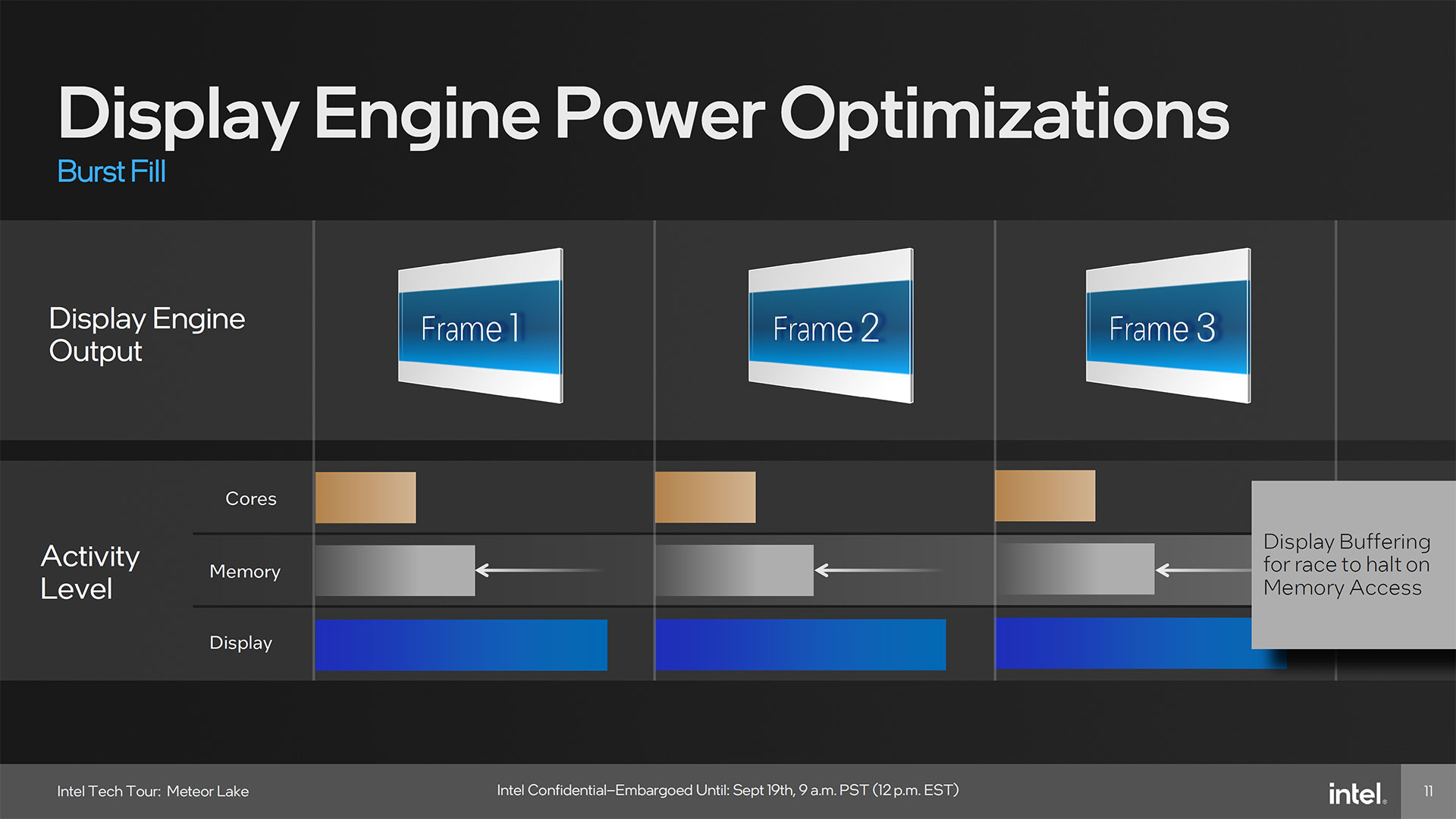
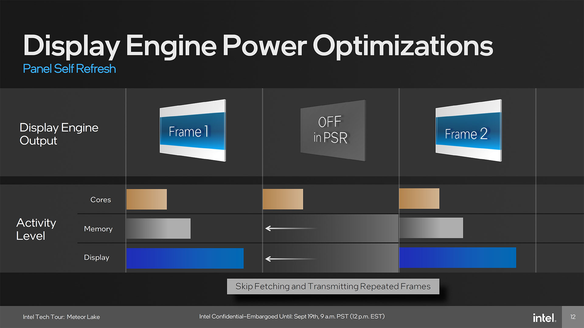
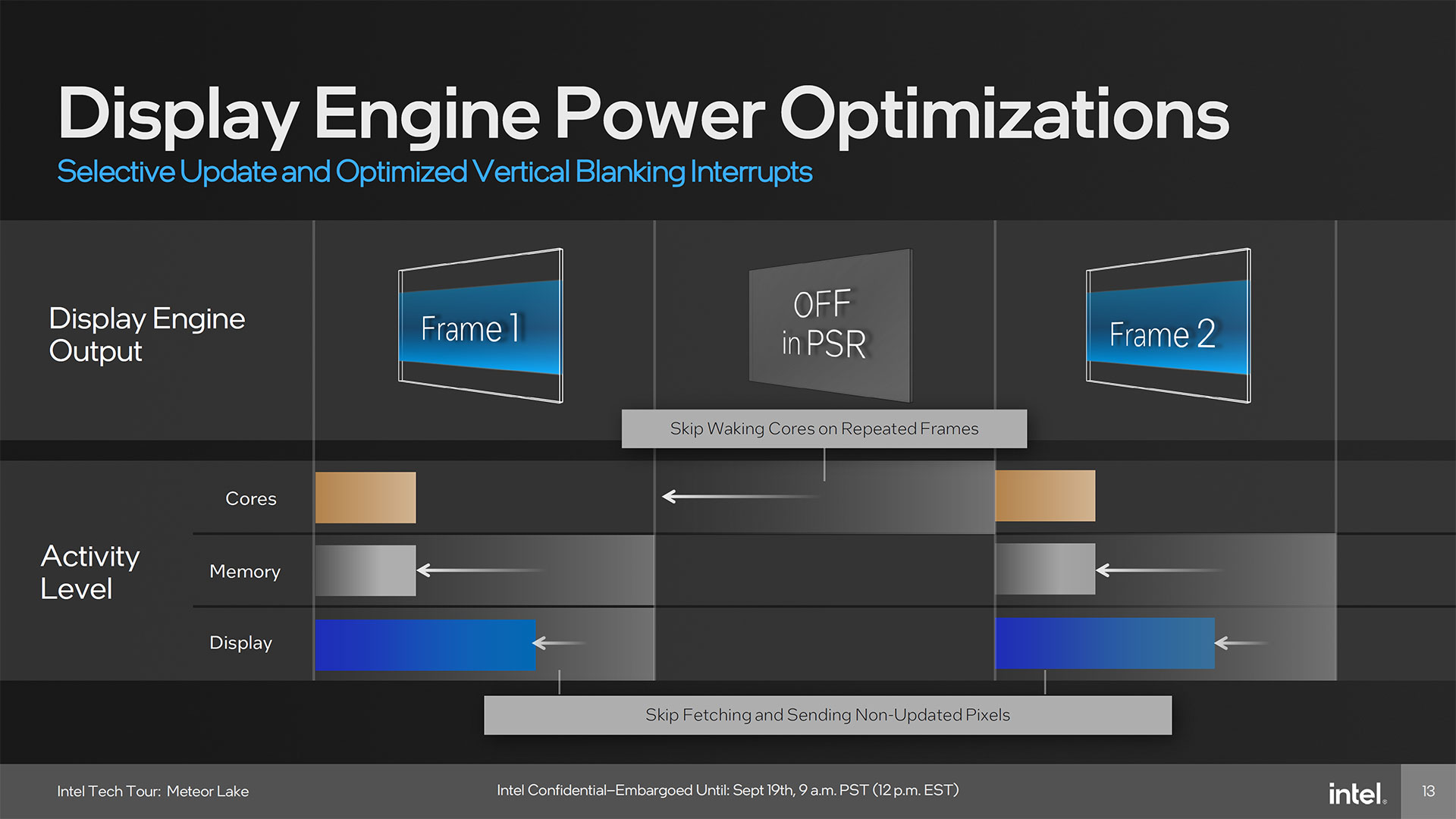
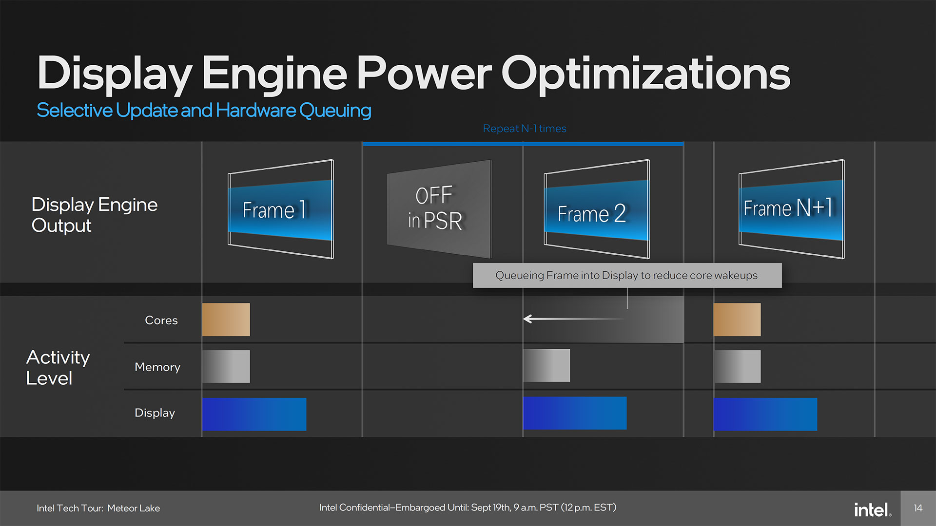
The low power optimizations work to avoid waking up cores, memory, and display elements when it's not necessary. For example, panel self refresh (PSR) in laptops doesn't need to fetch a new frame if it's just a repeat of the existing frame. Meteor Lake can also fetch only the updated portions of the display buffer — for example in Windows, you might be working in one window while everything else on the screen remained static.
One of the more interesting updates to the display engine is that Intel has added full support for DisplayPort 2.1 UHBR20 (20 Gbps per lane, 80 Gbps total). Arc GPUs only supported UHBR10, while AMD's RDNA 3 GPUs support UHBR13.5 (except for the professional W7900 that has UHBR20 on a single port). As we've noted before, Display Stream Compression (DSC) can already handle 4K 240Hz, but it's still good to have the latest display standards available.
Meteor Lake Software and Drivers
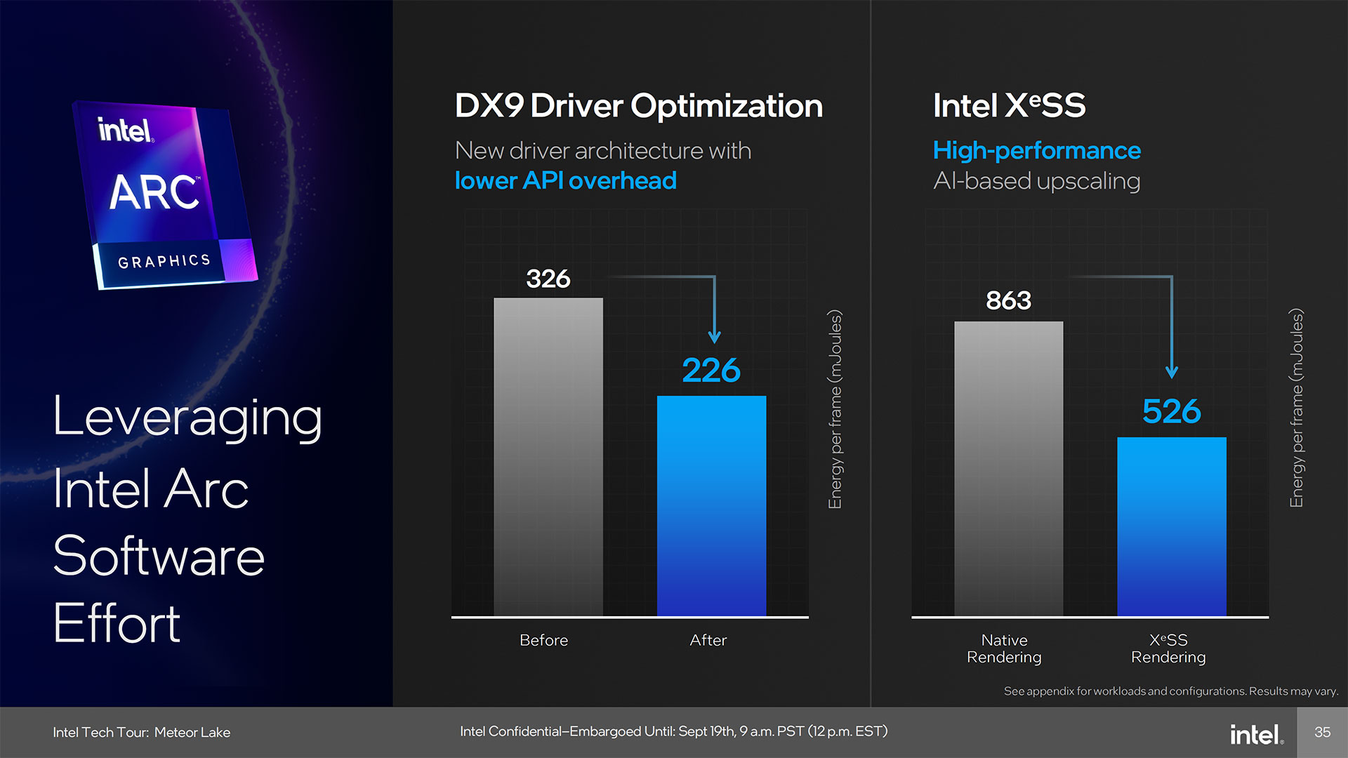
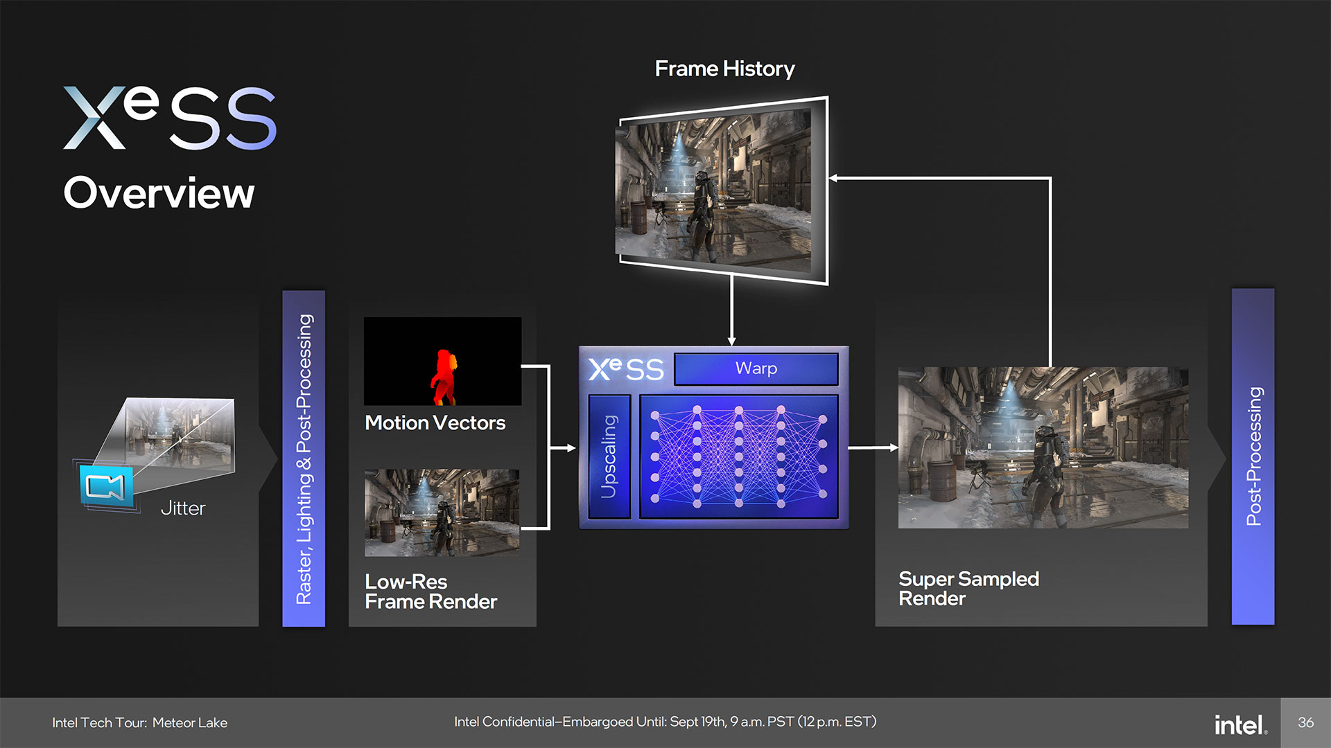
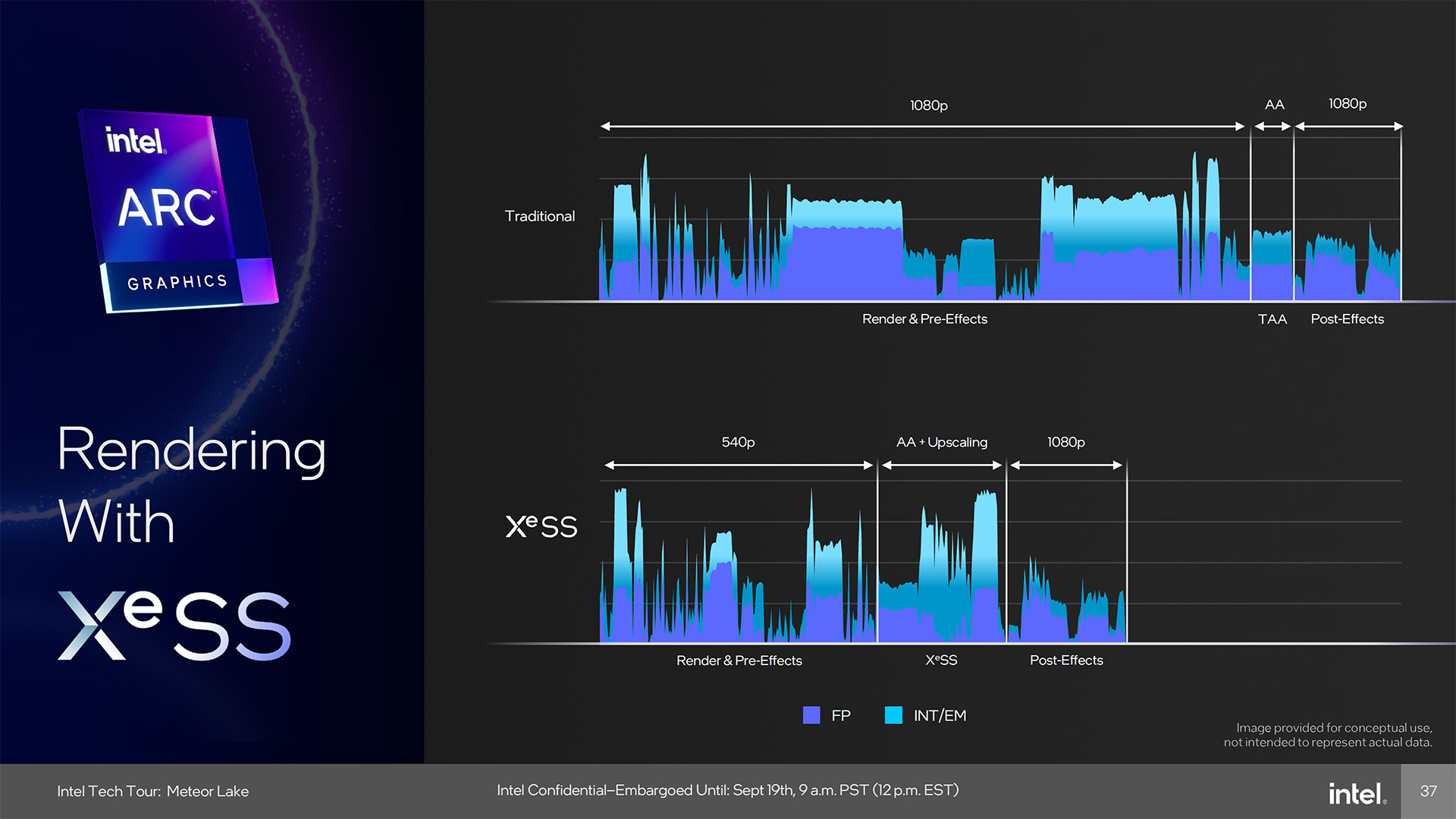
Wrapping things up, Intel also discussed some of the software stack (driver) improvements to its graphics suite. All of the improvements that have gone into Arc GPUs over the past year or so are also present with Meteor Lake graphics, including improved DX9 optimizations as well as DX11.
We mentioned XeSS already, and this has the potential to be quite useful on integrated graphics. Even 1080p at medium settings tends to be a bit much for integrated graphics, though with potentially Arc A380 levels of performance, it becomes a lot more viable. Toss in XeSS upscaling and some games might even reach 60 fps or more.
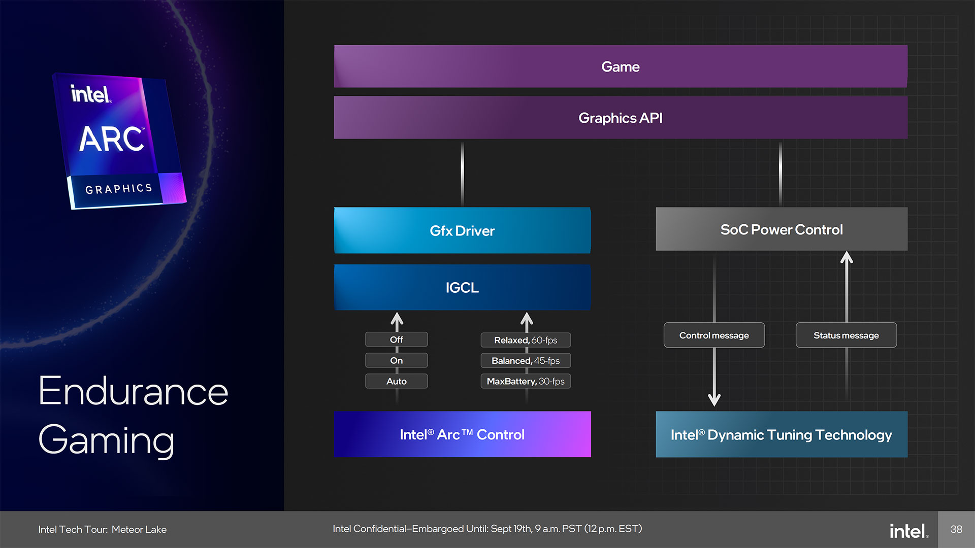
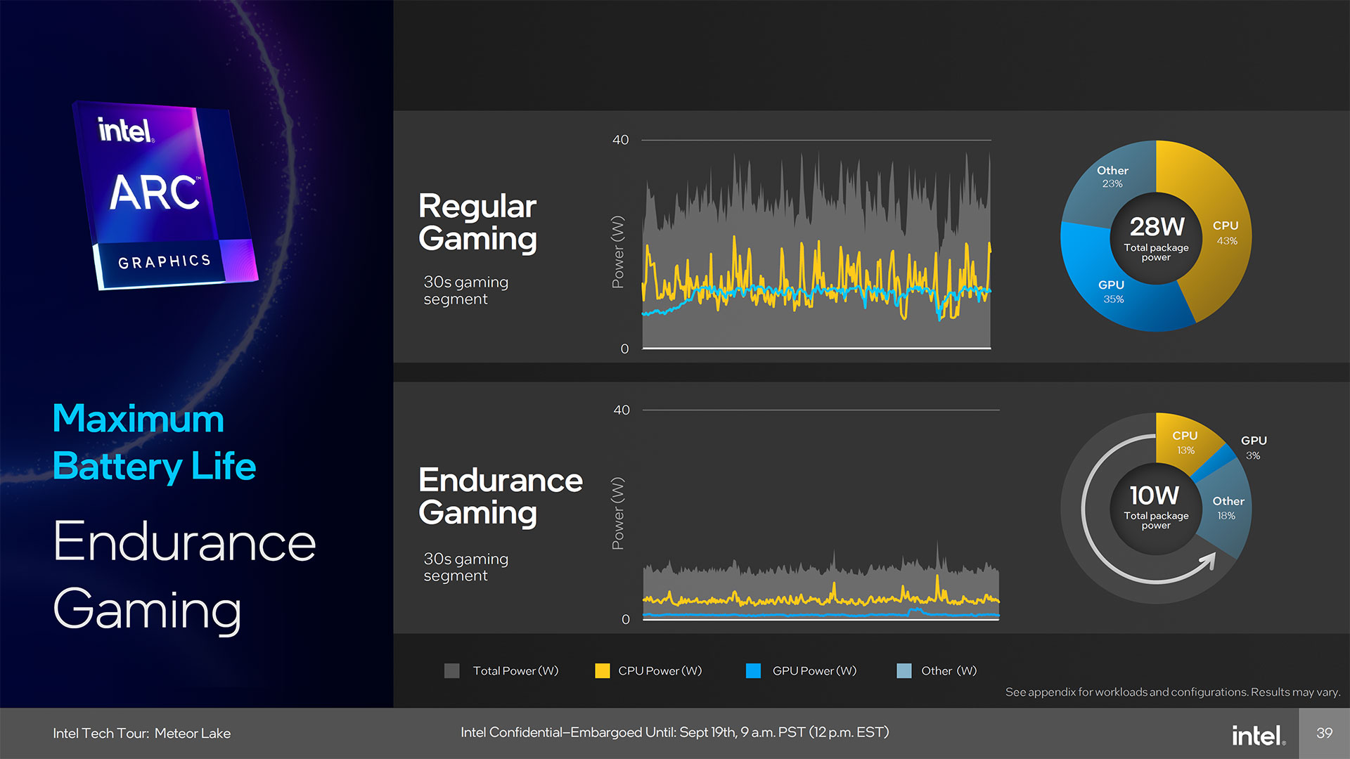
For laptops, Intel has also focused on "endurance gaming." In effect, various power optimizations, targeting lower frame rates, and tuning of CPU and GPU loads can help bring improved battery life. As an example, the normal way of running games would be to max out performance, and in that scenario a Meteor Lake processor might use 28W of power. With Endurance Gaming, that might drop to just 10W.
Take that with a helping of salt, however, as the 10W figure shows the CPU using 13%, GPU just 3% (what game is this supposed to be?), and Other at 18%. The slide references the appendix for details, which is also missing. Anyway, most 3D games tend to need a lot more from the GPU, and the amount you'll benefit from Endurance Gaming will vary based on the games you play.
Get Tom's Hardware's best news and in-depth reviews, straight to your inbox.

Closing Thoughts
Overall, there are some clear improvements to integrated graphics coming with Meteor Lake. Intel hasn't revealed the various product SKUs for Meteor Lake yet, though we do know it's launching on December 14. A lot of the discussion obviously focuses on laptops, and we're not sure what sort of graphics configurations will be present on the desktop chips — those almost certainly won't have the "integrated A380 lite" discussed above.
We expect the full-fat GPU will likely only appear with mobile chips. What will Intel use in desktop Meteor Lake? That's less clear. It could use a cut down version of the above, or more likely just leverage the existing Xe-LP / UHD 770 that's present in Alder Lake and Raptor Lake desktop chips. After all, if you want faster and more capable graphics for your desktop PC, there are plenty of dedicated GPUs available — including Arc.
We'll find out more on the specific MTL SKUs in the coming months. For your reference, the full Meteor Lake Graphics and Media slide deck can be found below.












Jarred Walton is a senior editor at Tom's Hardware focusing on everything GPU. He has been working as a tech journalist since 2004, writing for AnandTech, Maximum PC, and PC Gamer. From the first S3 Virge '3D decelerators' to today's GPUs, Jarred keeps up with all the latest graphics trends and is the one to ask about game performance.
-
bit_user @JarredWaltonGPU thanks for publishing this writeup. I missed it, at the time, but knew I'd come back to it when Meteor Lake finally launched.Reply
each Xe-Core comes with 16 Vector Engines. Those have the usual assortment of supported number formats, including FP32, FP16, INT8, and FP64 — the 64-bit support is a new feature, incidentally.
The fp64 support is for scalars, only. Calling it a "new feature" is only true in that it was initially dropped from Xe, but existed in prior generations of iGPU. fp64 is useful for certain geometry processing cases. Although it can be emulated, doing so would incur quite a performance penalty. I'm guessing the reason they re-added it is based on feedback from developers or from all the time they've spent investigating the various performance problems encountered by the Alchemist graphics cards. Whatever the reason, I'm glad to see its return, if only in scalar form.
One of the interesting aspects of the Meteor Lake "disaggregated architecture" is how the various elements that would normally be part of the GPU get scattered around the other tiles. The graphics tile handles everything discussed above, while the Display Engine and Xe Media Engine are part of the main SOC tile, and then the physical display outputs are part of the IO tile.
I believe the driving motivation behind this redistribution of blocks is to be able to power down the GPU tile, during activities like video playback.
Also, If I'm not mistaken, I think some of the display outputs are on the SoC tile, while others are on the I/O tile. If true, maybe the I/O tile can be kept in a low-power state when those displays aren't being used.
It includes encoding and decoding support for AVC, HEVC, VP9, and AV1 — the latter two being the new additions relative to prior Intel GPUs. It can handle up to 8K60 10-bit HDR decoding, and 8K 10-bit HDR encoding
It's funny, because their slide sort of implies it doesn't handle realtime AV1 encoding.
Also, the slide uses the ever-slippery weasel words "up to", when describing resolution and frame rate.
The low power optimizations work to avoid waking up cores, memory, and display elements when it's not necessary.
It sure sounds to me like they even went as far as integrating a chunk of DRAM into the display controllers, in order to avoid memory traffic. I won't quote the slides, but three of them contain the following annotations:
"Display buffering for race-to-halt on memory access" - okay, buffering where? "Skip fetching and sending non-updated pixels" - you can only do this if you've got the previous frame buffered somewhere.
"Queuing frame into display to reduce core wakeups" - again, the frame is being buffered somewhere!
So, am I right that their display controllers have builtin frame buffers, or is the buffer memory in panel controllers (with PSR) actually that flexible?
we're not sure what sort of graphics configurations will be present on the desktop chips
As you probably know, by now, the Meteor Lake desktop CPUs got canceled. Back when you published this article, perhaps it was still an unconfirmed rumor.
Here are some other questions I had, which I'm guessing you probably don't know the answers to, but I thought I'd mention, anyway.
So, when they say pairs of vector engines run in lock-step, does that mean they're fed by a dual-issue in-order instruction stream, as I think previous intel iGPU have done? Or is it more like they act in tandem, as an extended form of SIMD?
Also, what are Extended Math instructions? Do these consist of transcendental functions? Any others? -
JarredWaltonGPU Reply
It's all a bit fuzzy in my head now and I'd have to bone up on things again, but the slides are included for people like you. :-)bit_user said:@JarredWaltonGPU thanks for publishing this writeup. I missed it, at the time, but knew I'd come back to it when Meteor Lake finally launched.
I think there's (almost?) always limited FP64 support included, and maybe I had this wrong in the text.bit_user said:The fp64 support is for scalars, only. Calling it a "new feature" is only true in that it was initially dropped from Xe, but existed in prior generations of iGPU. fp64 is useful for certain geometry processing cases. Although it can be emulated, doing so would incur quite a performance penalty. I'm guessing the reason they re-added it is based on feedback from developers or from all the time they've spent investigating the various performance problems encountered by the Alchemist graphics cards. Whatever the reason, I'm glad to see its return, if only in scalar form.
Probably correct.bit_user said:I believe the driving motivation behind this redistribution of blocks is to be able to power down the GPU tile, during activities like video playback. Also, If I'm not mistaken, I think some of the display outputs are on the SoC tile, while others are on the I/O tile. If true, maybe the I/O tile can be kept in a low-power state when those displays aren't being used.
I do seem to recall asking about this, I guess I may need to follow up with Intel to confirm lack of AV1. It would be very disappointing if Intel ditched that just to save die space, but from a cost-savings perspective lack of AV1 encode probably doesn't matter that much.bit_user said:It's funny, because their slide sort of implies it doesn't handle realtime AV1 encoding. Also, the slide uses the ever-slippery weasel words "up to", when describing resolution and frame rate.
Good observation, I'm not sure on the details and I suspect Intel may be cagey about what exactly is going on for a reason (as in, protect its secrets).bit_user said:It sure sounds to me like they even went as far as integrating a chunk of DRAM into the display controllers, in order to avoid memory traffic. I won't quote the slides, but three of them contain the following annotations:
"Display buffering for race-to-halt on memory access" - okay, buffering where?"Skip fetching and sending non-updated pixels" - you can only do this if you've got the previous frame buffered somewhere.
"Queuing frame into display to reduce core wakeups" - again, the frame is being buffered somewhere!So, am I right that their display controllers have builtin frame buffers, or is the buffer memory in panel controllers (with PSR) actually that flexible?
Not sure on the first bit, but the Extended Math should be all the less common stuff like transcendental functions, square roots, and other complex bits and bobs. There's probably a white paper on it somewhere that says what the breakdown is for math that's "general" and supported on all the execution cores, and what stuff qualifies as "extended."bit_user said:Here are some other questions I had, which I'm guessing you probably don't know the answers to, but I thought I'd mention, anyway.
So, when they say pairs of vector engines run in lock-step, does that mean they're fed by a dual-issue in-order instruction stream, as I think previous intel iGPU have done? Or is it more like they act in tandem, as an extended form of SIMD?
Also, what are Extended Math instructions? Do these consist of transcendental functions? Any others? -
bit_user Reply
Xe/Alchemist did 100% drop hardware fp64! Intel's architecture slides on Xe showed that fp64 was "optional", but I can say it's definitely not in the Xe iGPU in Alder Lake, at least. I have also read that it's absent from Alchemist, but not confirmed it myself.JarredWaltonGPU said:I think there's (almost?) always limited FP64 support included, and maybe I had this wrong in the text.
If they patented it, then maybe not? I could go trolling through the patent database, but there's a limit to my curiosity.JarredWaltonGPU said:I suspect Intel may be cagey about what exactly is going on for a reason (as in, protect its secrets).
I do recall something about a patent indicating on-die DRAM and we speculated about it acting as a L4 cache. What if that was actually the frame buffer memory?
https://www.tomshardware.com/news/intel-patent-reveals-meteor-lake-adamantine-l4-cache
Thanks for the reply!
: )