New UCIe Chiplet Standard Supported by Intel, AMD, and Arm
Wiring it up
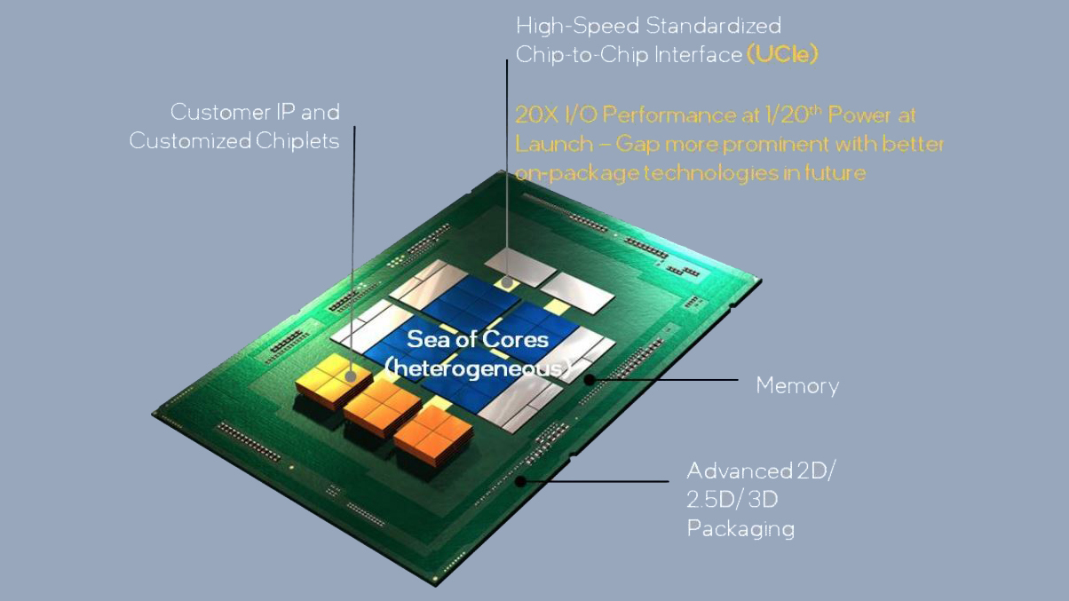
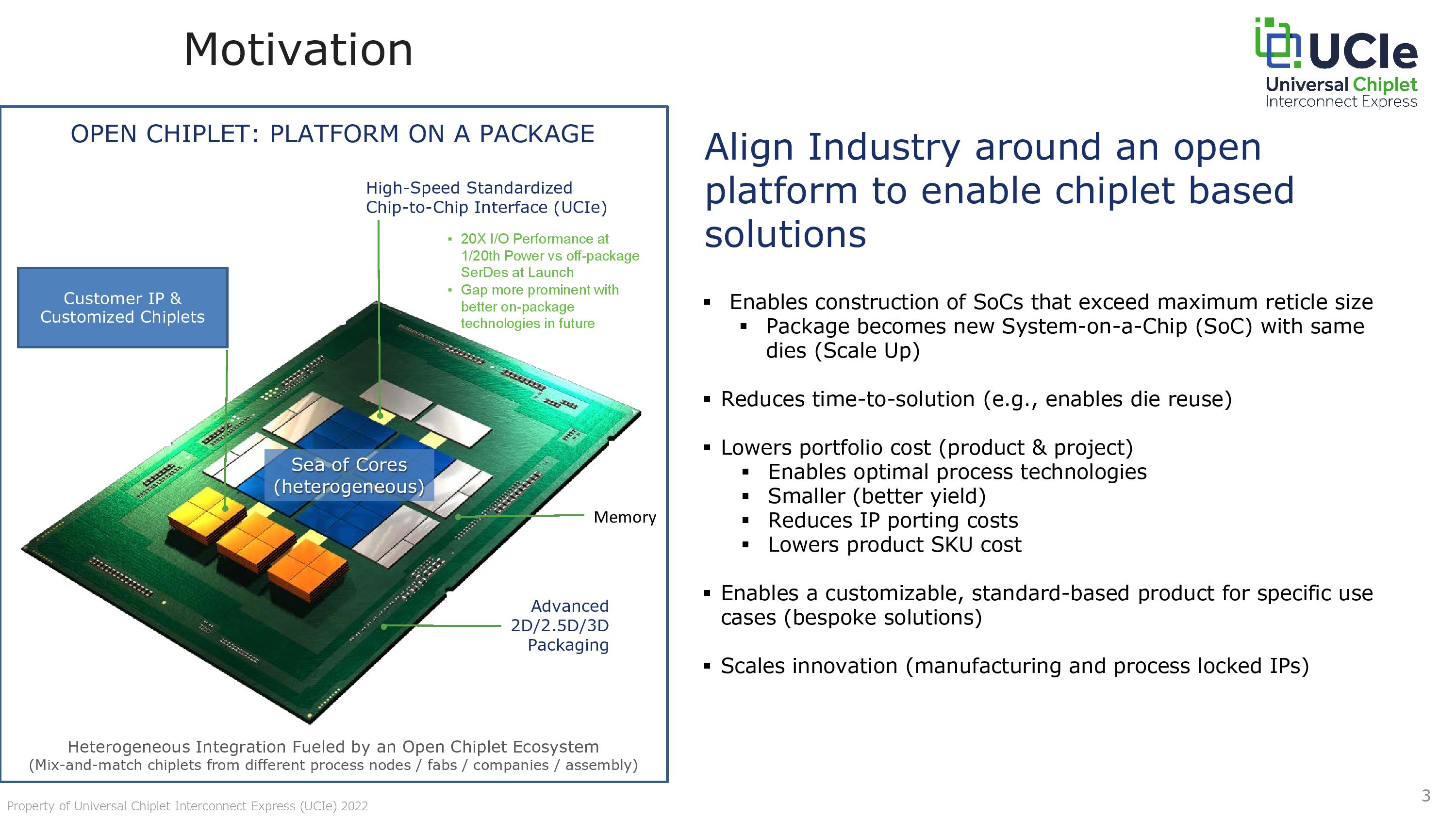
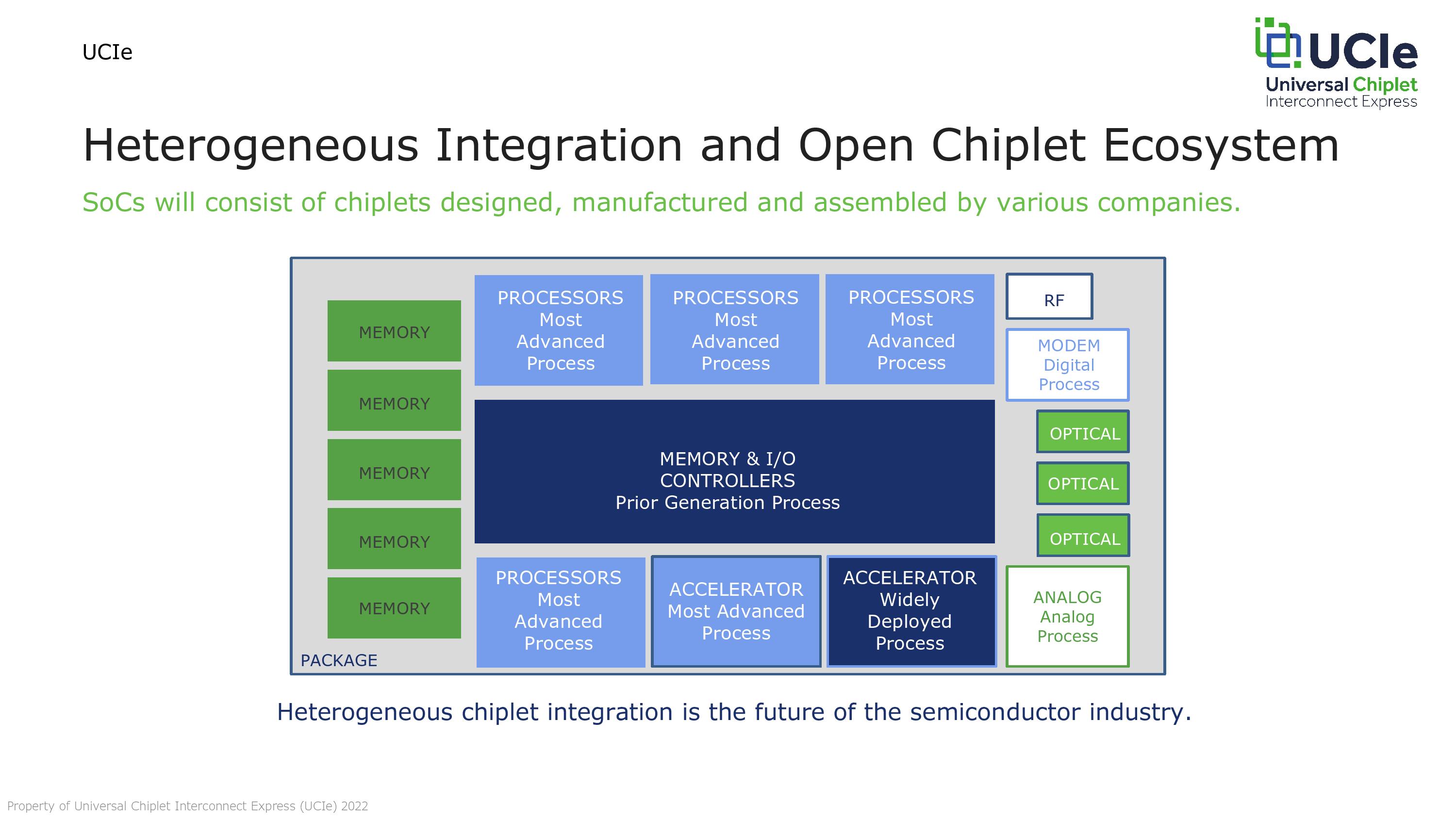
A broad range of industry stalwarts, like Intel, AMD, Arm, TSMC, and Samsung, among others, introduced the new Universal Chiplet Interconnect Express (UCIe) consortium today with the goal of standardizing die-to-die interconnects between chiplets with an open-source design, thus reducing costs and fostering a broader ecosystem of validated chiplets. In the end, the UCIe standard aims to be just as ubiquitous and universal as other connectivity standards, like USB, PCIe, and NVMe, while providing exceptional power and performance metrics for chiplet connections. Notably, all three of the leading foundries will adopt this tech, along with the x86 and Arm ecosystems (RISC-V and Nvidia are curiously absent).
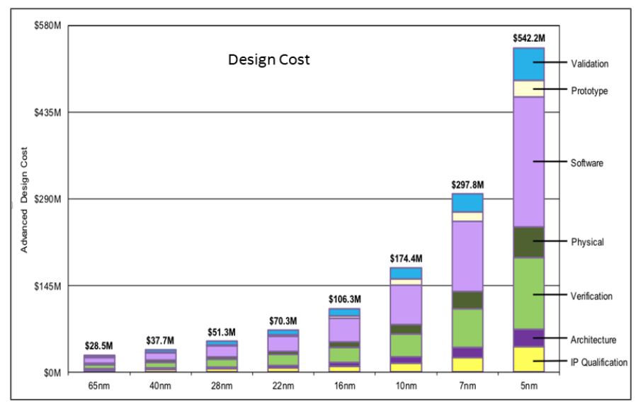
The benefits of chiplets, like reduced costs and using different types of process nodes in a single package, are well known and essential as chipmakers grapple with increasingly difficult scaling issues in the waning light of Moore's Law. The long-term vision for chiplets has always been for chipmakers to be able to develop their own types of specialized chiplets and then pair them with off-the-shelf chiplet designs from other companies, thus allowing them to build their own chips in Lego-like fashion to improve time to market while reducing costs.
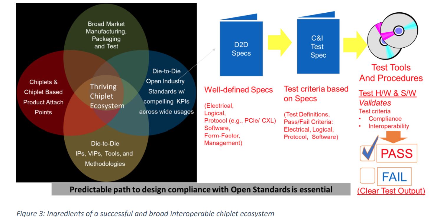
However, the lack of a standardized connection between chiplets has led to a wide range of customized proprietary interconnects, so modern chiplets certainly aren't plug-and-play with other designs. Additionally, the industry has long suffered from a glaring lack of standardized validation and verification for chiplet designs and interconnects, making an off-the-shelf chiplet ecosystem impossible.
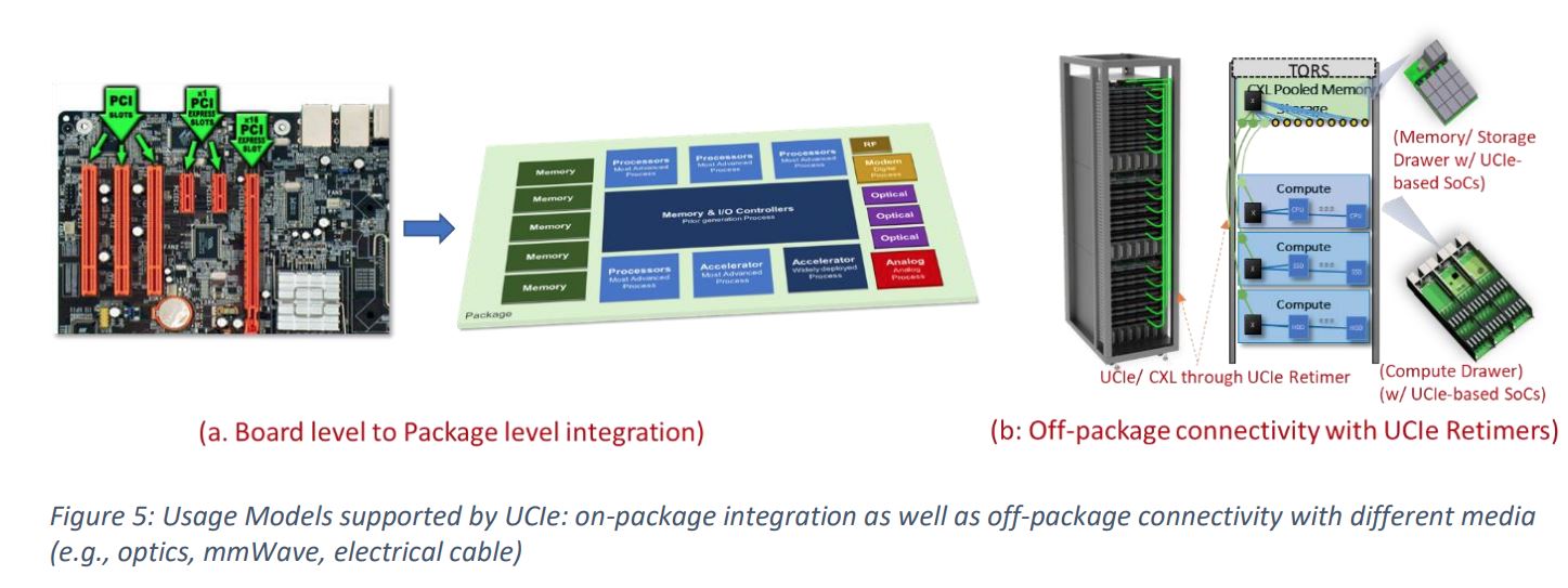
This new UCIe interconnect will enable a standardized connection between chiplets, like cores, memory, and I/O, that looks and operates similar to on-die connections while also enabling off-die connections to other componentry — the designs can even enable low enough latency and high enough bandwidth for rack-scale designs – and relies on existing protocols, like PCIe and CXL.
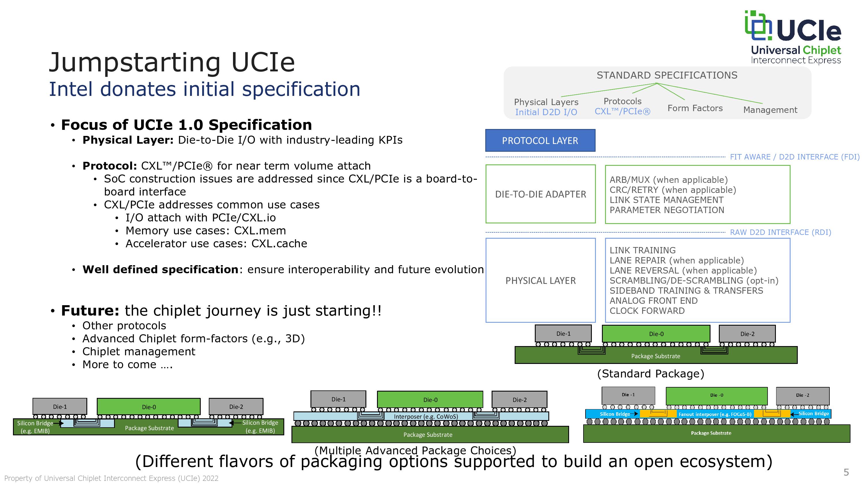
UCIe is a layered protocol with a physical layer and a die-to-die adapter. As you can see in the second slide, the physical layer can consist of all types of current packaging options from multiple companies. That includes standard 2D packaging and more advanced 2.5D packaging like Intel's silicon-bridge EMIB, TSMC's interposer-based CoWoS, and fanout interposer approaches, like FOCoS-B. The UCIe standard will also eventually expand to 3D packaging interconnects in the future.
A protocol layer runs on top of the physical layer, and the initial specification relies upon PCIe or the open Compute eXpress Link (CXL - originally donated by Intel) protocol. The PCIe protocol provides wide interoperability and flexibility, while CXL can be used for more advanced low latency/high throughput connections, like memory (cxl.mem), I/O (cxl.io), and accelerators such as GPUs and ASICs (cxl.cache). While the specification begins with PCIe and CXL as the current protocols, it will expand to include other protocols in the future.
Intel had previously used two interface IP blocks for EMIB; the Advanced Interconnect Bus (AIB) and UIB. Intel donated AIB as an open-source royalty-free standard in a previous attempt to foster a standardized chiplet ecosystem, but that didn't gain much industry traction. However, UCIe and AIB are not inherently interoperable (special subset designs can enable the use of both), so while Intel will continue to support current AIB implementations fully, it will stop all further development and migrate to UCIe.
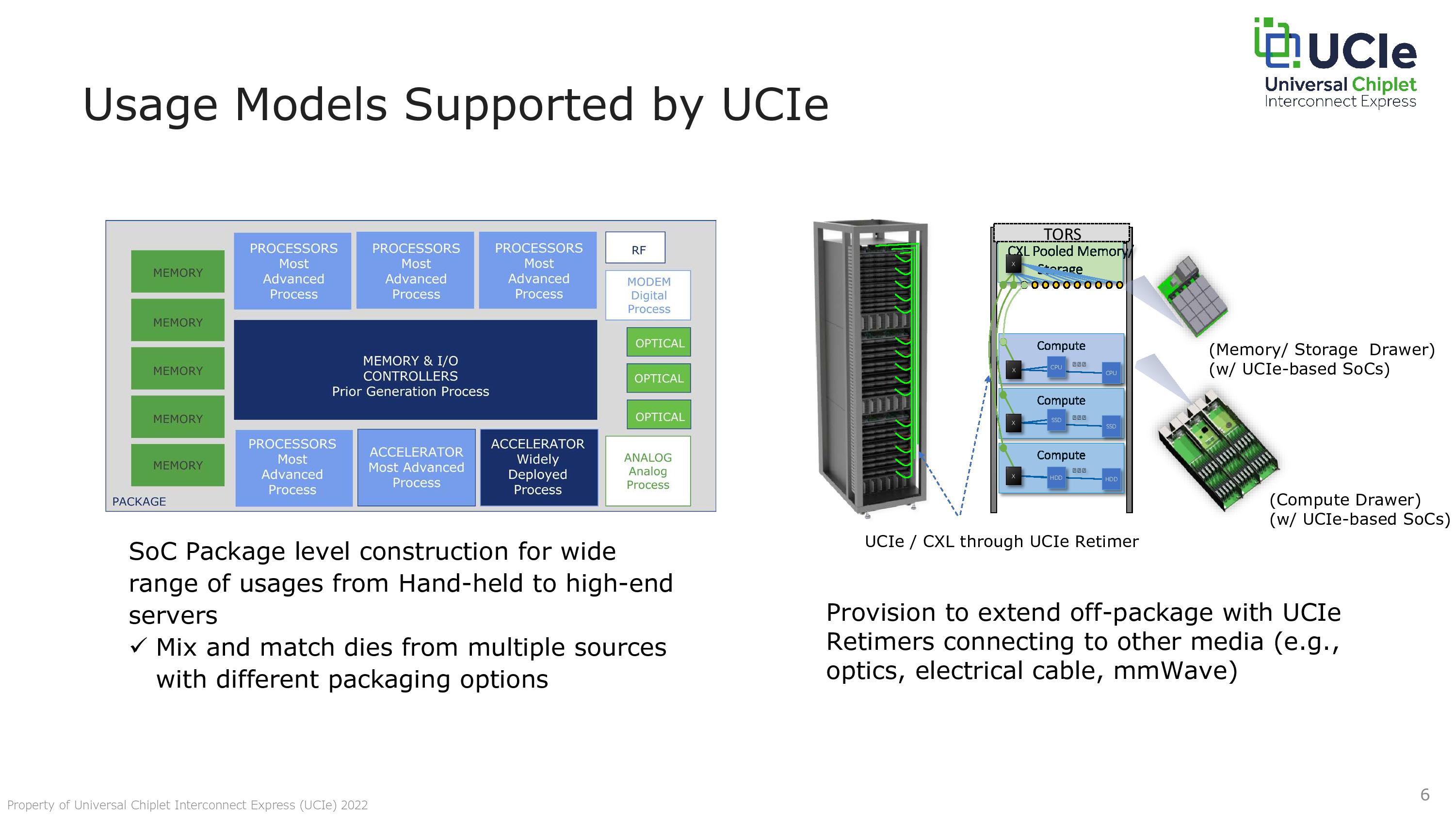
The UCIe specification also includes a retimer design that can extend the connection off the chip package, enabling optical and electrical connections to other componentry, such as pooled memory, compute, and accelerator resources. Given the excellent performance metrics (which we'll cover below), the UCIe consortium envisions the interconnection eventually enabling the types of rack-scale disaggregated systems the industry has struggled to build in meaningful quantities for decades. The die-to-rack connections could use native CXL for PCIe for communication (no translations required), perhaps finally providing the latency and bandwidth required for such designs. Additionally, other types of protocols can be used if required.
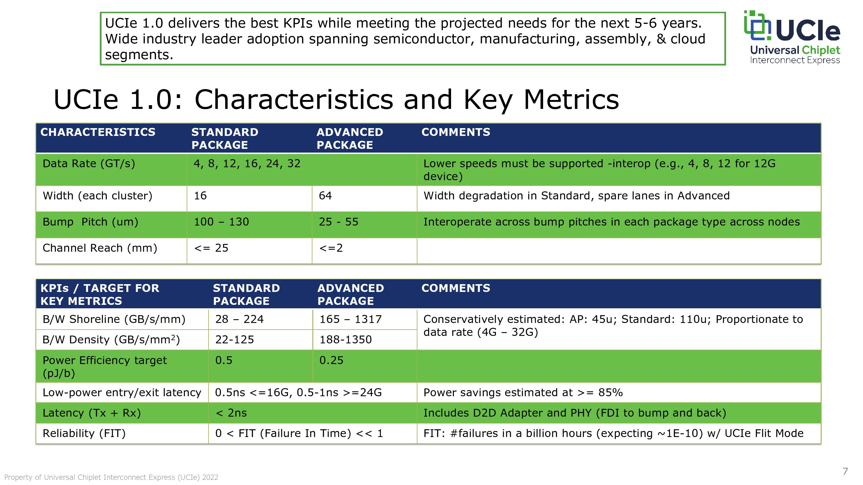
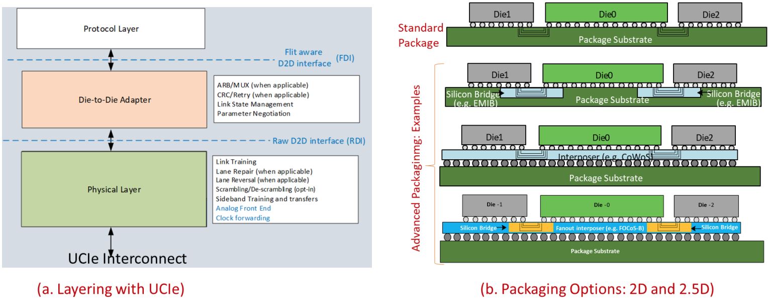
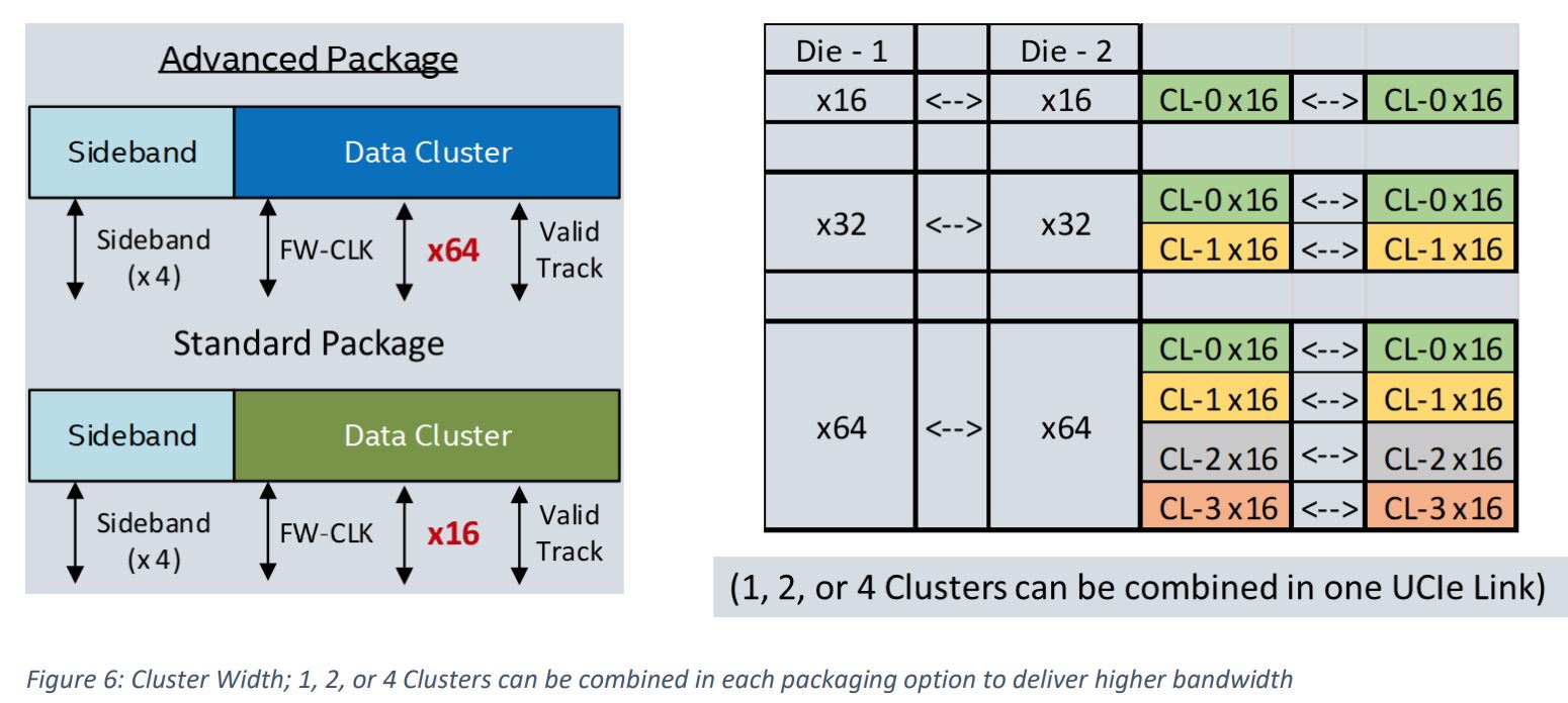
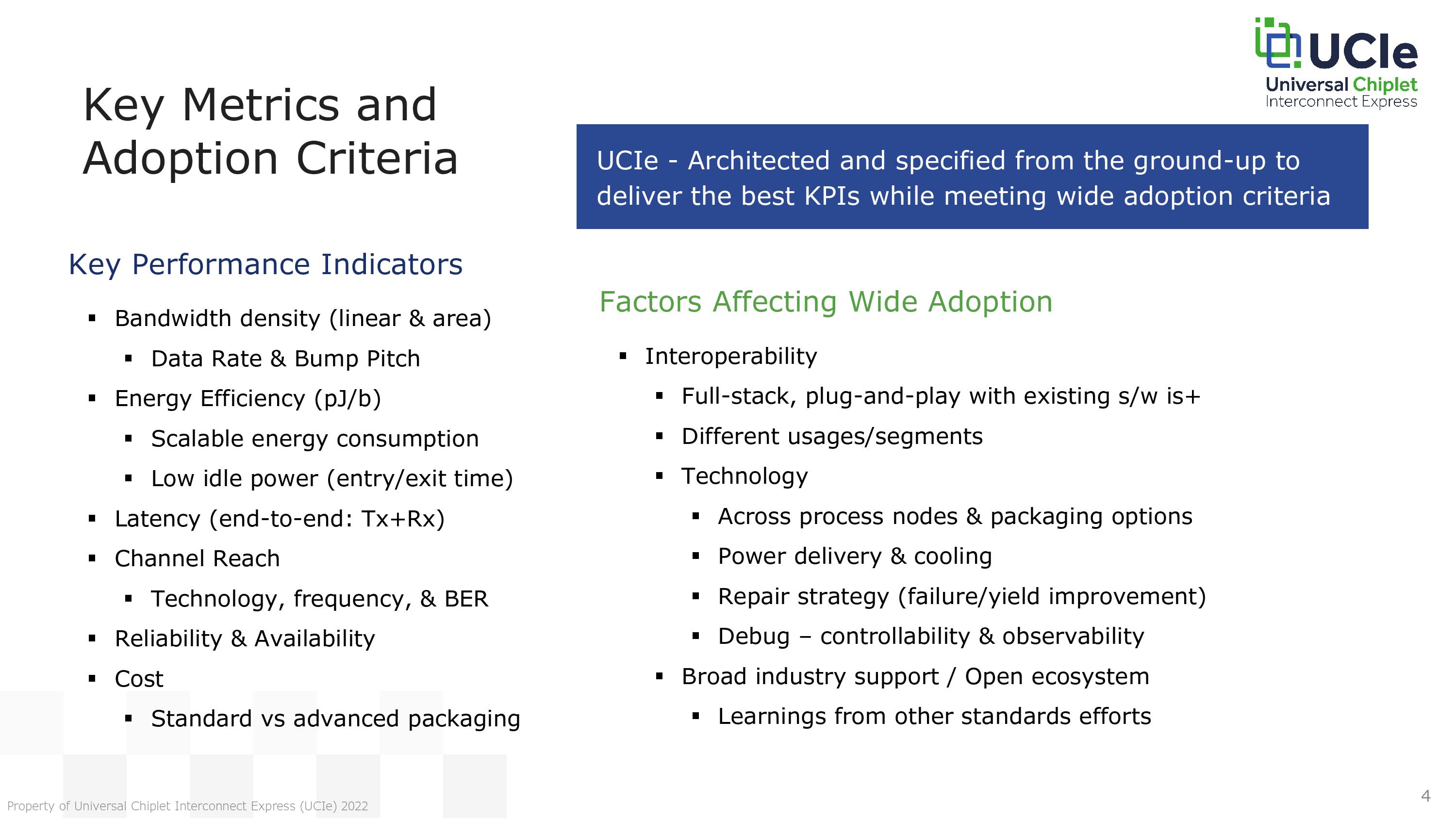
The consortium has outlined very aggressive performance and area targets, and there are many moving parts to tailor the connection for a broad range of uses — not just the highest-end devices. The consortium carves the targets into two broad ranges, with standard 2D packaging techniques and more advanced 2.5D techniques (EMIB, CoWoS, etc.). Naturally, the advanced packaging options provide higher bandwidth and density.
Configurable factors include data rate (spans 4 to 32 GT/s), width (lane counts), bump pitch (density of the connections), and channel reach (length of the physical connection). Latency weighs in at sub-2-nanoseconds. Notably, channel reach extends from 2mm, enabling very close die alignments, to 25mm for longer-reach applications. However, like the other metrics outlined in the first slide, these are just the primary targets. For instance, a designer could simply drop the frequency to extend the connection further than 25mm.
For the highest-performance devices, it's often all about cramming in as much low-latency bandwidth as possible into the smallest area possible. However, most designs don't require that level of performance, so there are multiple levers that designers can pull to customize their designs. As such, the 'target for key metrics' section in the first slide will vary based on the various design choices.
For instance, the BW Shoreline (GB/s per MM) and BW density (GBs per mm^2) projections are based on a 45-micron bump pitch. However, the spec supports bump pitches as low as 25 microns, which would then increase these values by a factor of three or more. That means we could see up to 3.8 TB/s of throughput per mm^2 for a UCIe connection. However, relaxing those values can increase power efficiency, highlighting the multiple optimization axes available to meet just about any use case. Additionally, the consortium built the spec with power efficiency in mind, accommodating advanced features like fast entry/exit (sub-nanosecond scale) from power-on and power-off states.
Overall, the UCIe spec aims to make the on-package interconnects look as similar to on-die interconnects as possible while providing a plethora of options that can enable just about any type of performance or packaging tech required. However, the UCIe spec does have a competitor in the Open Compute Project's Bunch of Wires (BoW) spec. The BoW spec is designed to also democratize chiplet designs and boasts impressive performance specifications, but it isn't quite as flexible. For instance, BoW offers power efficiency of 0.7 to 0.5 pJ/bit (Picojoules per bit), while the various levers available with UCIe enable anywhere from 0.5 to 0.25 pJ/bit. (This can vary by process node used.)
The BoW spec supports a fixed 16 GT/s, while UCIe is configurable and stretches up to 32 GT/s. UCIe also leads in other metrics, like Shoreline Bandwidth density (1280 Gbps vs up to 3.8 Tb/s) and is also limited to MCP packaging, while UCIe can support the majority of 2D and 2.5D packaging options.
Standardizing the interconnect is one of the first steps to improving any device's broader validation, compliance, and interoperability. Unfortunately, the semiconductor industry has long suffered from a lack of widely-accepted validation, verification, and qualification processes for chiplets, thus hampering wider adoption. The UCIe consortium has a keen focus on these aspects, with a chapter of the initial UCIe 1.0 spec targeted at validation and in-built features, like a dedicated side-band channel, to help with these efforts.
Overall, the UCIe spec looks promising, but widespread support is critical. As we saw with the CXL spec that is now table stakes in the industry (will be supported by Intel Sapphire Rapids, AMD's EPYC Genoa, and Arm designs), the consortium comes to market with a list of blue-chip sponsors, and we expect this list to grow just as quickly as CXL.
Sponsors include AMD, Intel, Samsung, Arm, ASE, TSMC, Google, Meta, Microsoft, and Qualcomm. That's an impressive list that includes the top three foundries, which is important. Notably, Nvidia isn't currently participating and we see no signs of RISC-V, either.
The UCIe 1.0 specification is available now, and the consortium also has a website with a whitepaper and other resources.
Get Tom's Hardware's best news and in-depth reviews, straight to your inbox.

Paul Alcorn is the Editor-in-Chief for Tom's Hardware US. He also writes news and reviews on CPUs, storage, and enterprise hardware.
-
nopslide this stuff sounds interesting but way over my head. what exactly is a chiplet, how do they impact stuff for consumer or server level hardware?Reply
my understanding is that this is part of a move from general purpose CPUs to specialized chips for lots of little things - like say matrix multiplies for AI or video decoders or crypto miners. this common standard would let different players specialize in different sorts of chiplets and bundle it all into one chip that say a consumer building their own PC or a mobile phone manufacturer could buy. is that sort of in the right ballpark? -
InvalidError Reply
Chiplet/tile designs have three key benefits:nopslide said:my understanding is that this is part of a move from general purpose CPUs to specialized chips for lots of little things
by breaking down large chip design into multiple smaller parts, each part can be tested separately to reduce the amount of wafer space lost on fill factor (you can fill a wafer closer to the edge with smaller dies) and the amount of space lost on dies with fatal defects on them
you can mix-and-match processes to use the best process available for things that generally cannot be done on one single chip without massive compromises, ex.: DRAM requires a low-leakage process that produces transistors too slow for high-speed logic, chiplets lets you bring the two processes together in one design and
you can create a whole product range out of semi-standard legos, which could possibly include more semi-custom options like what you mentioned.
The downside is that chip-to-chip interconnects do add chip manufacturing complexity, latency and consume more die area than monolithic, especially when you add standardized protocol layers in-between. So as far as CPU designs are concerned, I doubt they will be breaking those down smaller than compute clusters sharing their local L3 cache like AMD has been doing with Zen 2/3. -
nopslide ReplyInvalidError said:Chiplet/tile designs have three key benefits:
by breaking down large chip design into multiple smaller parts, each part can be tested separately to reduce the amount of wafer space lost on fill factor (you can fill a wafer closer to the edge with smaller dies) and the amount of space lost on dies with fatal defects on them
you can mix-and-match processes to use the best process available for things that generally cannot be done on one single chip without massive compromises, ex.: DRAM requires a low-leakage process that produces transistors too slow for high-speed logic, chiplets lets you bring the two processes together in one design and
you can create a whole product range out of semi-standard legos, which could possibly include more semi-custom options like what you mentioned.The downside is that chip-to-chip interconnects do add chip manufacturing complexity, latency and consume more die area than monolithic, especially when you add standardized protocol layers in-between. So as far as CPU designs are concerned, I doubt they will be breaking those down smaller than compute clusters sharing their local L3 cache like AMD has been doing with Zen 2/3.
Oh okay, so it sounds like the purpose of these designs is about better internal manufacturing efficiencies and not necessarily something that translates directly into a consumer visible change beyond price then. Thanks i appreciate the answer. -
InvalidError Reply
And you could add:nopslide said:Oh okay, so it sounds like the purpose of these designs is about better internal manufacturing efficiencies and not necessarily something that translates directly into a consumer visible change beyond price then. Thanks i appreciate the answer.
4) (as a corollary to #1) with defects limited to smaller pieces of silicon eliminating the high risk of massive monolithic designs especially on cutting-edge processes, it also enables the fabrication of multi-die monstrosities like Ponte Vecchio (40+ active tiles) and whatever even more ambitious projects are likely to follow.