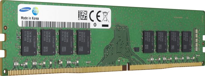
Samsung B-die memory chips are pretty much considered the holy grail for hardware enthusiasts and overclockers. You can imagine the hardware community's disappointment when word got out that Samsung was retiring its B-die offerings in favor of the company's more recent A-die memory chips.
Samsung used to produce the famed B-die memory chips on the 20nm manufacturing process. With A-die, the memory manufacturer is moving to a more recent 10nm-class node. Sadly, memory products with A-die are still pretty scarce at the moment. There isn't sufficient data to see whether A-die is better or worse than its predecessor.
The Samsung A-die DDR4 module, which was spotted by a Hardwareluxxx reader, is identified by the M378A4G43AB2-CVF part number. It's a dual-rank stick with a capacity of 32GB. If you recall, one of A-die's promises is to offer higher density per module. The Samsung module is rated to run at 2,933 MHz with CL21-21-21 timings and a 1.2V operating voltage. The memory speed is pretty decent, but the timings certainly leave a lot to be desired. However, keep in mind that the A-die is still wet behind the ears; the timings will most likely improve in time.
MemoryCow, a United Kingdom memory and storage retailer, has listed the Samsung M378A4G43AB2-CVF module for £128.33, excluding VAT (Value Added Tax). So, we can expect to see the module costing around $157.77, which would be the cheapest DDR4-2933 32GB module on the market. The only other stick that has identical specifications comes from Crucial, and it commands a $171.99 price tag.
Get Tom's Hardware's best news and in-depth reviews, straight to your inbox.

Zhiye Liu is a news editor, memory reviewer, and SSD tester at Tom’s Hardware. Although he loves everything that’s hardware, he has a soft spot for CPUs, GPUs, and RAM.
-
digitalgriffin Dual rank? That means additional latency in memory timings.Reply
That's surprising. Isn't that reserved for mem sticks with lots of chips slapped on them? I thought with the node shrink higher capacity would be put on a single chip and not multiple chips. It would keep the die small, and raise the yield rate, but at the cost of access times.
Or is my understanding incorrect? (All the memory timing specs are still somewhat a mystery to me.)
