Samsung 3D Stacks 12-Layer HBM2E Chips, Now 24GB of Capacity
Get Tom's Hardware's best news and in-depth reviews, straight to your inbox.
You are now subscribed
Your newsletter sign-up was successful
The HBM2E standard -- relevant for graphics cards, servers, high-performance computing and more -- pledges up to 24GB and 307 GBps of memory bandwidth per stack, and Samsung is ready to fulfill that promise. The South Korean giant announced today its development of the industry’s first 12-layer 3D-TSV chip packaging technology, which will enable the company to produce 24GB HBM2E (High Bandwidth Memory Generation 2 Enhanced) chips.
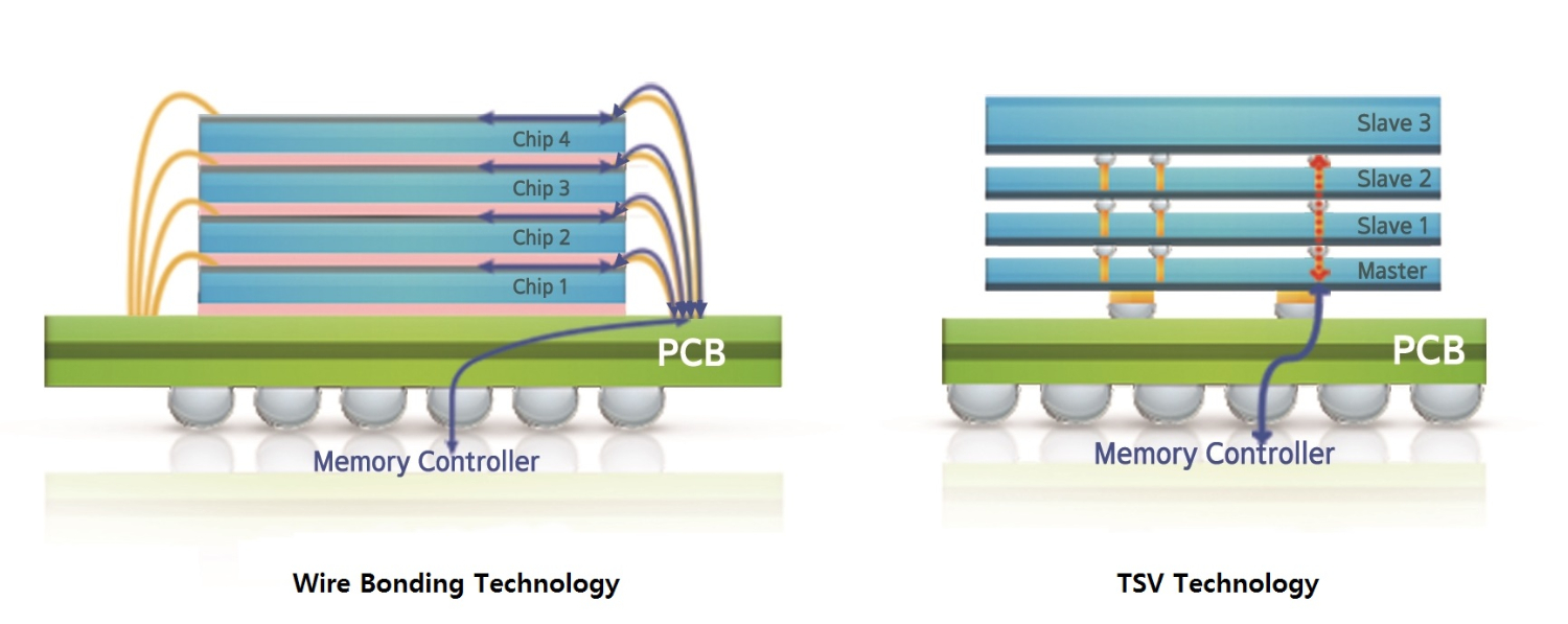
Samsung's new 12-layer 3D-TSV (through-silicon bia) technology basically allows the company to stack up to 12 DRAM chips while retaining the same thickness of 720 micrometers as the brand's current 8-layer HBM2 solution. This is great news for manufacturers, as they will be able to take advantage of the higher capacity chips without needing to modify their configuration designs. Samsung said that the 12 DRAM chips are vertically interconnected through a 3D configuration comprised of over 60,000 TSV holes that are 1/20th the thickness of a strand of human hair.
The four extra layers will allow Samsung to pack up to 24GB of memory on a single package, which is up to three times the capacity of existing 8GB HBM2 products. The company's 12-layer 3D-TSV technology not only paves the way for higher capacity HBM chips, but also boosts performance, thanks to the shorter transmission times and lower power consumption.
Article continues belowSamsung will start mass-producing its 24GB HBM2E products shortly, so we won't be surprised if upcoming high-end graphics cards start to utilize Samsung's new offerings.
Get Tom's Hardware's best news and in-depth reviews, straight to your inbox.

Zhiye Liu is a news editor, memory reviewer, and SSD tester at Tom’s Hardware. Although he loves everything that’s hardware, he has a soft spot for CPUs, GPUs, and RAM.

