Samsung Shares Plans for 2nm and 1.4nm Chips
Samsung reveals process technologies roadmap.

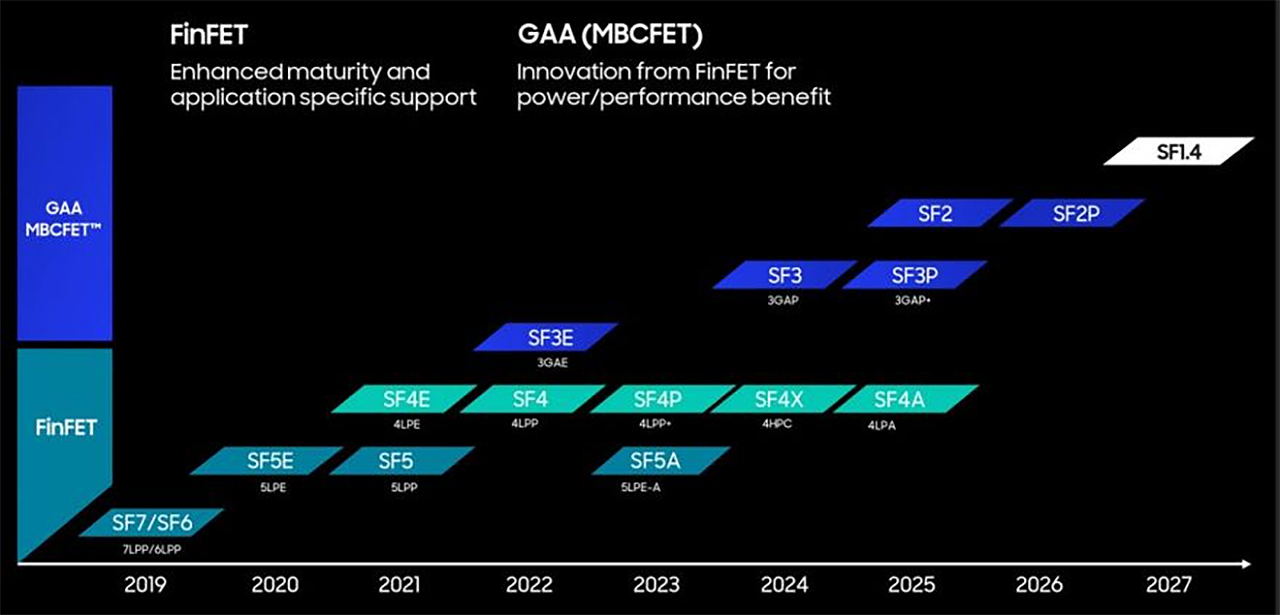
Samsung unveiled its updated fabrication technology roadmap at its annual Samsung Foundry Forum (SFF) 2023. The company is on track to produce chips on its its 2nm and 1.4nm-class nodes in 2025 and 2027, respectively. In addition, the company intends to add a leading-edge 5nm-class radio frequency manufacturing process and start making GaN chips in the coming years.
Samsung expects its SF2 (2nm-class) fabrication technology to provide a 25% higher power efficiency (at the same frequency and transistor count), a 12% higher performance (at the same power and complexity), and a 5% decrease in area (at the same transistor count) when compared to SF3 (2nd Generation 3nm-class), the company revealed at SFF 2023. The company will start making mobile SoCs on 2nm node in 2025 and in follow up with HPC-enhanced SF2P node in 2026. Meanwhile, SF1.4 (1.4nm-class) manufacturing process is projected to be available to Samsung's customers in 2027.
To make its SF2 node more competitive, Samsung intends to ensure that its customers will have access to a collection of high-quality SF2 IPs shortly, including interfaces like LPDDR5x, HBM3P, PCIe Gen6, and 112G SerDes.
In addition to offering leading-edge technologies for smartphone, client PC, and datacenter SoCs, Samsung also plans to offer specialized fabrication processes in the coming years. This includes SF2A tailored for automotive applications in 2027, and 5nm Radio Frequency (RF) node in 2025. Compared to current generation 14nm RF process, the upcoming 5nm RF is anticipated to enhance power efficiency by 40% and boost transistor density by approximately 50%.
Samsung is also set to commence manufacturing of gallium nitride (GaN) power semiconductors in 2025. These chips will be targeted at a variety of applications, ranging from consumer electronics to data centers and the automobile industry.
Samsung Foundry is not only focusing on broadening its technology portfolio, but also on enhancing its manufacturing capacities in the U.S. and South Korea. The company plans to initiate high volume production of chips at its Pyeongtaek line 3 (P3) in the second half of 2023. As for the fab in Taylor, Texas, it is on track to finish construction by the end of the year, and its operations are projected to begin in the second half of 2024 (probably very late 2024).
As part of its ambitious goals, the contract maker of chips intends to enhance its total clean room capacity 7.3-fold by 2027, a substantial increase compared to the capacity it owned in 2021.
Get Tom's Hardware's best news and in-depth reviews, straight to your inbox.

Anton Shilov is a contributing writer at Tom’s Hardware. Over the past couple of decades, he has covered everything from CPUs and GPUs to supercomputers and from modern process technologies and latest fab tools to high-tech industry trends.
-
The Historical Fidelity Glad to see Samsung sticking with official metric length scales (IE nanometer) instead of using the obsolete Angstrom for “market differentiation”. I’m tired of people telling me Intel will release their advanced 20A process when TSMC will only be at the 2nm. News flash 20A = 2nm.Reply -
anticeon This is so funny because latest 4mm samsung only have yield rate of 40% compared to 75% TSMCReply -
bit_user Reply
That must be per unit of area. Any idea what area?anticeon said:This is so funny because latest 4mm samsung only have yield rate of 40% compared to 75% TSMC
