SK Hynix Starts Manufacturing 1anm DRAM Using EUV Lithography
Another major DRAM improvement.

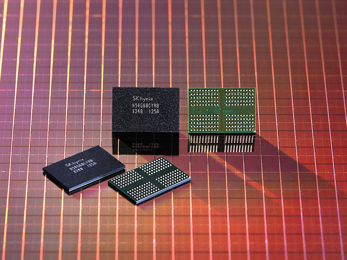
SK Hynix, a South Korean giant, has today announced that the company has officially started manufacturing its 1anm DRAM products using Extreme ultraviolet (EUV) lithography technology. The first product to be manufactured on this process is an 8 Gigabit (Gb) LPDDR4 mobile DRAM chip.
Running at speeds of 4266Mbps, the fastest for LPDDR4 standard, this new chip achieves up to 20% less power consumption thanks to the new process. To show just how effective the 1anm process is, SK Hynix claims that EUV enables it to gain 25% more chips on the same size wafer, translating into 25% density improvement.
The 1anm process is SK Hynix's fourth iteration of 10 nm technology used for DRAM manufacturing. Its predecessors included 1x, 1y, and 1z processes, all of which are based on the 10 nm node, just with some tweaking applied to newer generations. The new 1anm EUV process has shown stability in manufacturing, and the company plans to use it for all of its products going forward.
The first DRAM product based on this process is the aforementioned 8Gb LPDDR4 chip, which is currently in mass production. It is expected to reach the market as a part of smartphones sometime in the second half of 2021. The 1anm DRAM technology will also apply to DDR5 products made by SK Hynix, starting early next year.
SK Hynix also notes that the product is helping the company accomplish its goal to "reduce carbon dioxide emission as part of its commitment to the environmental, social and governance (ESG) management". Cho Youngmann, Vice President at SK hynix, has commented on that announcement that “With improved productivity and cost competitiveness, the latest 1anm DRAM will not only help secure high profitability, but also solidify SK hynix’s status as a leading technology company with early adoption of the EUV lithography technology for mass production.”
Get Tom's Hardware's best news and in-depth reviews, straight to your inbox.