Toshiba Shows 64-Layer BiCS FLASH At Dell World
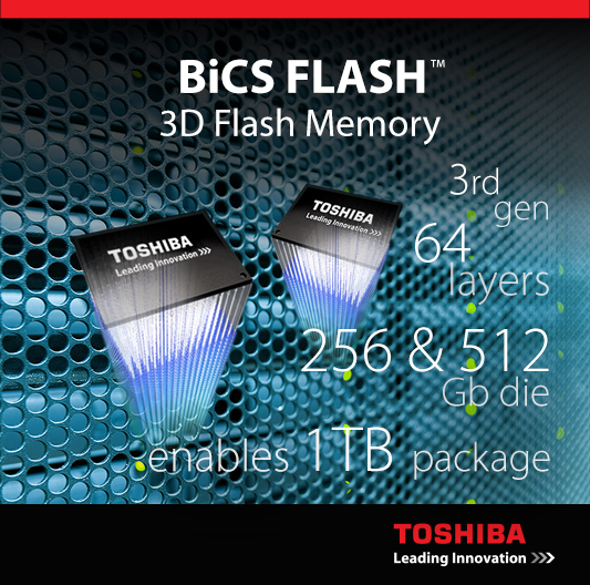
Toshiba introduced the world to third-generation 3D flash using Toggle2 today at Dell World. At the Toshiba booth, you can see firsthand a notebook running BiCS FLASH--which is Toshiba's name for 3D NAND technology that now sports 64 layers and a massive density that puts a full terabyte of storage into a single die stack.
We first tested BiCS FLASH in our initial DRAMless SSD Roundup and believe it's the only third-party test using the technology. The reference design prototype from Phison used second-generation BiCS. That product eventually shipped in a limited number of products, including some Apple iPhones and a Toshiba BGA single package SSD using package on package (PoP) technology for an OEM customer.
Toshiba's new third generation is set to take the world by storm. The crossover from planar (2D) to 3D disrupted the supply chain because several NAND manufacturers transitioned at the same time. The new technology increases die density from 128Gbit to 256Gbit--and even 512Gbit for higher-capacity devices.
Article continues belowUsing third-generation BiCS means SSD manufacturers can build consumer and enterprise SSDs with up to 1TB of capacity for each package. On the consumer side, we often see products with eight and even 16 packages on the circuit board. Once available, and after the early yield issues are resolved, we should get out of the NAND shortage with higher-capacity and cheaper products.
Before Dell World, we spoke with Toshiba about the new technology. Using advanced error correction code, enterprise users can expect up to 10,000 program erase cycles with BiCS FLASH. Toshiba is currently migrating all client, data center, and enterprise SSDs over to 64-layer 3D TLC memory. The new flash is faster than planar memory and can program up to three pages per cycle. BiCS uses a dual-plane interface to the controller.
We don't want to omit the fact that no one is talking about multi-level cell BiCS. Last year, we spoke with SanDisk and learned that the company saw MLC as the past and TLC as the future. Western Digital's first high-performance NVMe SSD gave the words real meaning, even though most users called foul.
“Toshiba SSDs powered by the 64-layer 3D device and in-house controller increase value to our customer’s products by boosting the maximum offered drive capacities and presenting superior speed, performance and endurance” said Shigenori Yanagi, SSD technology executive, at Toshiba Memory Corporation.
Get Tom's Hardware's best news and in-depth reviews, straight to your inbox.
The real question for many is how long it will be before this technology makes its way to end user devices like consumer SSDs. We've seen a Phison road map for controllers with 3D-ready controllers set for early 2018. Computex is just a few weeks out, so we'll have more details soon on Toshiba's (and even Micron's) 64-layer products.

Chris Ramseyer was a senior contributing editor for Tom's Hardware. He tested and reviewed consumer storage.
-
drwho1 ReplyUsing third-generation BiCS means SSD manufacturers can build consumer and enterprise SSDs with up to 1TB of capacity for each package. On the consumer side, we often see products with eight and even 16 packages on the circuit board. Once available, and after the early yield issues are resolved, we should get out of the NAND shortage with higher-capacity and cheaper products.
If I read this correctly, this means a 16TB SSD is possible. -
chaz_music "Last year, we spoke with SanDisk and learned that the company saw MLC as the past and TLC as the future."Reply
Great article, Chris. Just one note. TLC implies three logic levels per cell, and MLC is undefined as Multiple Level Cell. The industry has to go forward with higher and higher bit levels to get cost down. The 3D approach is a packing evolution but it still requires the same basic manufacturing and die growth to make. That means the cost is still about the same per GB to manufacture = same cost to consumer per GB.
Sandisk has an X4 line that is 4 bits per cell. So their quote is probably a miscommunication on their part. But - it is exciting to see these technologies developing.
- Charles -
Rookie_MIB Reply19667284 said:Using third-generation BiCS means SSD manufacturers can build consumer and enterprise SSDs with up to 1TB of capacity for each package. On the consumer side, we often see products with eight and even 16 packages on the circuit board. Once available, and after the early yield issues are resolved, we should get out of the NAND shortage with higher-capacity and cheaper products.
If I read this correctly, this means a 16TB SSD is possible.
Possible? Certainly. Affordable? That's the debatable part.
Overall the thing I do see with the transitioning to stacked cells is that the TLC endurance can be extended quite a bit as the larger lithography is more forgiving and allows for a higher program/erase count. What is still very much open to debate though is still -speed-. So many of the lower priced TLC drives really perform quite poorly compared to the MLC drives (with a few notable exceptions) and from what I see it's not an issue with controller hardware - but more of an issue with the nature of trying to accurately program a TLC data cell with a very exact voltage to represent the bit-state.
