TSMC Dishes on 5nm and 3nm Process Nodes, Introduces 3DFabric Tech
TSMC puts Intel in the rearview

TSMC's 26th Technology Symposium kicked off today with details around its progress with its 7nm N7 process, 5nm N5, N4, and 3nm N3 nodes. TSMC also shared details around its 3DFabric technology and provided some clues about what technologies it will use to continue scaling beyond the 3nm node. TSMC has already disrupted the pecking order of the semiconductor industry when it brushed aside Intel and Samsung and moved to its industry-leading 7nm node, powering Intel's competitor AMD (among others) to the forefront. Still, the company shows no signs of slowing down its rapid pace of innovation and has plans to begin high volume production of its 3nm tech in 2022, compared to Intel's plans to debut its 7nm in late 2022 or early 2023.
TSMC's 5nm 'N5' process employs EUV technology "extensively" and offers a full node scaling benefit over N7. TSMC claims the N5 process offers up to 15% more performance (at the same power) or 30% power reduction at the same performance, and a 1.8X logic density gain over the 7nm N7 process. TSMC also says the defect density learning curve for N5 is faster than N7, meaning the 5nm process will reach higher yield rates quicker than its predecessor.
| Improvement | 5nm 'N5' over 7nm 'N7' | 5nm 'N5P' over N5 | 5nm 'N4" over N5 | 3nm 'N3' over 5nm 'N5' |
| Power at Same Performance | 30% | 10% | ? | 25-30% |
| Performance at Same Power | 15% | 5% | ? | 10-15% |
| Density Improvement | 1.8X | ? | ? | 1.7X |
| Risk / High Volume Manfacturing | In HVM | Ramp in 2021 | Risk 4Q21 / HVM 2022 | Risk 2021 / HVM 2H22 |
TSMC also has its enhanced N5P node in development for high performance applications, with plans to ramp in 2021. N5P offers 5% more performance (as iso-power) or a 10% reduction in power (at iso-performance) over N5.
Article continues belowFounder and CEO of Ampere Computing Renee Jones presented at the event and said the company already has its next server chip being fabbed on the N5 process, so it's clear TSMC has already jumped most of the 5nm design hurdles.
For 5nm, TSMC says it's ramping N5 production in Fab 18, its fourth Gigafab and first 5nm fab. The company certainly isn't wasting any time speeding past its competitors — one year after breaking ground in 2018, TSMC began moving in over 1,300 fab tools, completing that task in just eight months. Fab 18 began volume production of N5 in the second quarter of 2020 and is designed to process approximately one million 12-inch wafers per year.
Because it is IP-compatible with the N5 node, TSMC's 5nm N4 process offers a straightforward migration with unspecified performance, power, and density enhancements. TSMC was light on the details, but we do know that it requires fewer mask layers. TSMC plans to begin N4 risk production in the fourth quarter of 2021, with high volume production targeted for 2022.
The company also said its 3nm N3 node would begin risk production in 2021 and hit high volume manufacturing (HVM) in the second half of 2022. This node offers full node scaling over N5 and will bring up to a 10-15% performance improvement or 25-30% power reduction paired with an (up to) 1.7X density improvement. The node continues to use the FinFET architecture and offers a 1.2X increase in SRAM density and a 1.1X increase in analog density.
Get Tom's Hardware's best news and in-depth reviews, straight to your inbox.
TSMC also covered its N12E process, which is designed specifically for low-power devices, like IoT, mobile, and edge devices, while improving density. It supports ultra-low leakage devices and ultra-low Vdd designs down to 0.4V.
TSMC shared a few additional details of its 7nm node, which started production in 2018 and has powered many high-performance chips from the likes of AMD, Apple and others. The company repeated its claim of shipping 1 billion good dies on the node, highlighting that it has enjoyed excellent yields while powering much of the industry with a leading-edge node that beats out both Intel and Samsung. The company has already taped out over 140 designs, with plans for 200 devices by the end of the year.
The company's N7+ meanwhile is the world's first node to adopt EUV in high volume manufacturing, and the backward-compatible N6 offers up to an 18% logic density improvement. TSMC says N6 already has the same defect density as N7. Combined with less complexity, N7+ is already yielding higher than N7.
TSMC Possibly Moving Beyond Silicon for Sub-3nm
TSMC is also working to define its next node beyond N3 and shared some of the industry advances that could help it move beyond 3nm, but didn't provide any specifics of which technologies it would employ. TSMC listed nanosheets and nanowires among the advances, along with new materials, like high mobility channels, 2D transistors, and carbon nanotubes as candidates that it is already researching.
TSMC has more than 15 years of experience with nanosheet technologies and has demonstrated that it can yield working 32Mb nanosheet SRAM devices that operate at 0.46V. TSMC has also identified several non-silicon materials suitable for 2D that could scale channel thickness below 1nm. The company is also working with carbon nanotube devices.
TSMC continues to deepen its investments in research and development, with $2.96 billion invested in 2019 alone, and the company is building a new R&D center staffed with 8,000 engineers next to the company headquarters. The first phase of that project will be complete in 2021.
TSMC Advanced 3D Packaging Technologies: Meet 3DFabric


Mirroring what we've heard from other industry players, TSMC believes that advanced packaging technologies are the key to further density scaling, and that 3D packaging technologies are the best path forward.
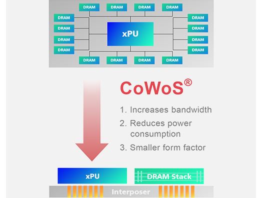
TSMC already has a robust portfolio of 3D packaging technologies in its wafer-level 3DIC technologies, like Chip-on-Wafer-on-Substrate (CoWoS), Integrated Fan Out (InFO-R), Chip on Wafer (COW), and Wafer-on-Wafer (WoW). The company is now rolling these technologies under a new "3DFabric" umbrella, which appears to be a new branding scheme for its 3D packaging technologies that tie together chiplets, high bandwidth memory, and specialized IPs into heterogeneous packages.
TSMC aligns the 3DFarbic hierarchy into front-end 3D stacking technologies under its SoIC group (CoW and WoW), and aligns the back-end 3D stacking technologies into the InFO and CoWoS subgroups. This collection of technologies enables a myriad of packaging options. TSMC has developed new LSI (Local SI Interconnect) variants of its InFO and CoWoS packaging that merit further coverage in another article. For now, head here for more info.
TSMC's Tech Symposium consists of a selection of pre-recorded videos, so we'll have further updates as we work through more of the material.

Paul Alcorn is the Editor-in-Chief for Tom's Hardware US. He also writes news and reviews on CPUs, storage, and enterprise hardware.
-
Endymio 3nm is two full process nodes ahead of 5nm ... and only netting TSMC a 10-15% performance increase? That seems a bit paltry, doesn't it?Reply -
ingtar33 ReplyEndymio said:3nm is two full process nodes ahead of 5nm ... and only netting TSMC a 10-15% performance increase? That seems a bit paltry, doesn't it?
with 30% more power efficiency -
Endymio Reply
One of us is reading that chart wrong. I read it as mutually exclusive: 10-15% more performance at the same power draw, or 30% less power at the same performance. Not both at once.ingtar33 said:with 30% more power efficiency -
hannibal Well people have to remember that these Numbers Are pure marketing so 3nm is not even same ballpark with real 3nm... so the improvements Are Also smaller . In reality these still Are about 40 to 54 nm in reality...Reply -
Afrospinach From what I understand "3nm" does not necessarily mean what it has traditionally meant and more of a marketing label, perhaps as is mentioned above why the improvements seem underwhelming. 3nm is half the size of 7nm, that is huge. In the past that has meant an almost linear half power consumption.Reply -
Endymio Reply
Certainly with current understanding it is (though as previous posters have pointed out, current process nanometer nomenclature is essentially marketing rather than actual physical size). I do recall plenty of stories in the late '90s that anything below 100 nm was essentially impossible. So at some point in the future, we very well may see transistors of 3nm or even smaller ... though quite probably through some process rather than lithography.nofanneeded said:correct me if I am wrong , isnt true 3nm impossible to reach ? -
nofanneeded ReplyEndymio said:Certainly with current understanding it is (though as previous posters have pointed out, current process nanometer nomenclature is essentially marketing rather than actual physical size). I do recall plenty of stories in the late '90s that anything below 100 nm was essentially impossible. So at some point in the future, we very well may see transistors of 3nm or even smaller ... though quite probably through some process rather than lithography.
I know that scientists made ~0.18nm transistor using 13 atoms around a molecule which is the theoretical limit , and cannot be made into a whole chip ... but I dont know why they say 3nm is the limit actually.