Wafer-Scale Heterogeneous Chips May Pave the Way Beyond Moore's Law
A forward-looking solution in the computing route may include wafer-sized chips packing a number of different IP blocks.

The journey of Moore's Law is a technologically complex and expensive one, worth billions of dollars in research and development - just ask semiconductor manufacturers. The much-referred-to "soft" law coined by Intel co-founder Gordon Moore stated that the number of transistors in a densely-packed semiconductor should double every two years. The death of Moore's Law has been hailed time and time again, and is now understood as more of a target rather than a rule - yet it's a necessary goalpost for silicon designers to compare against. The ever-increasing transistor densities have posed many challenges for system designers, however - there are always limitations imposed by physics and the current level of technology that define a hard limit to how many transistors can be pushed into a single chip. And as transistor density and chip sizes increase, the impact of manufacturing defects (which may render parts of the chips inoperative) also has to be taken into account.
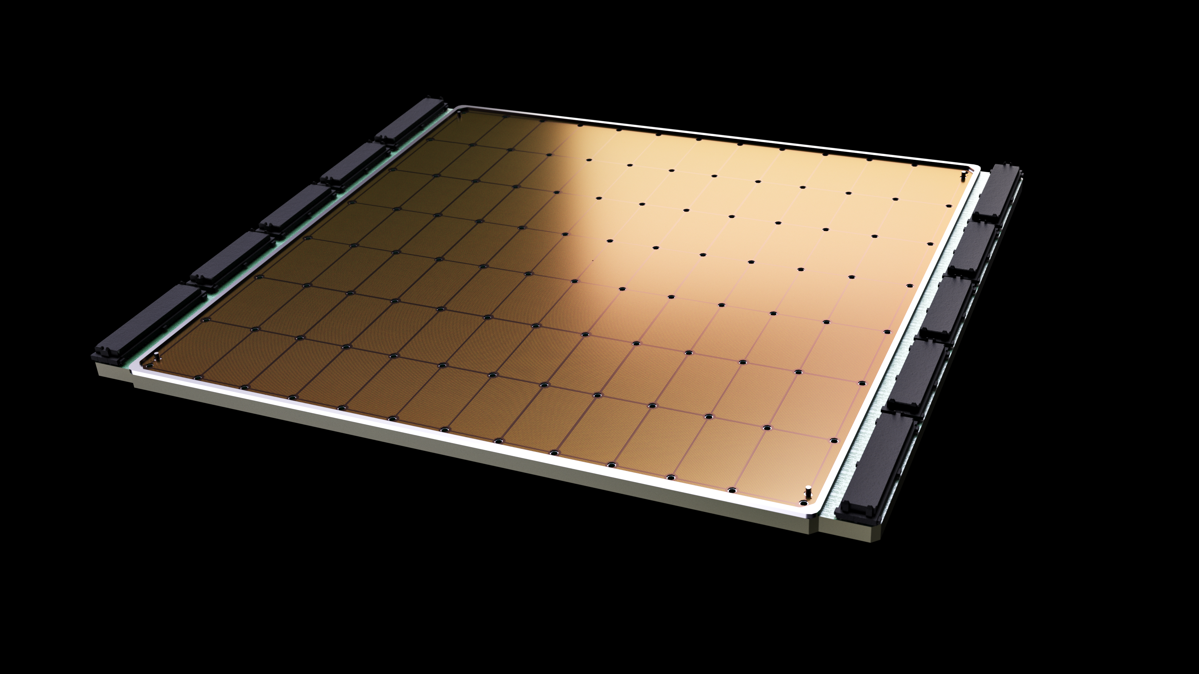
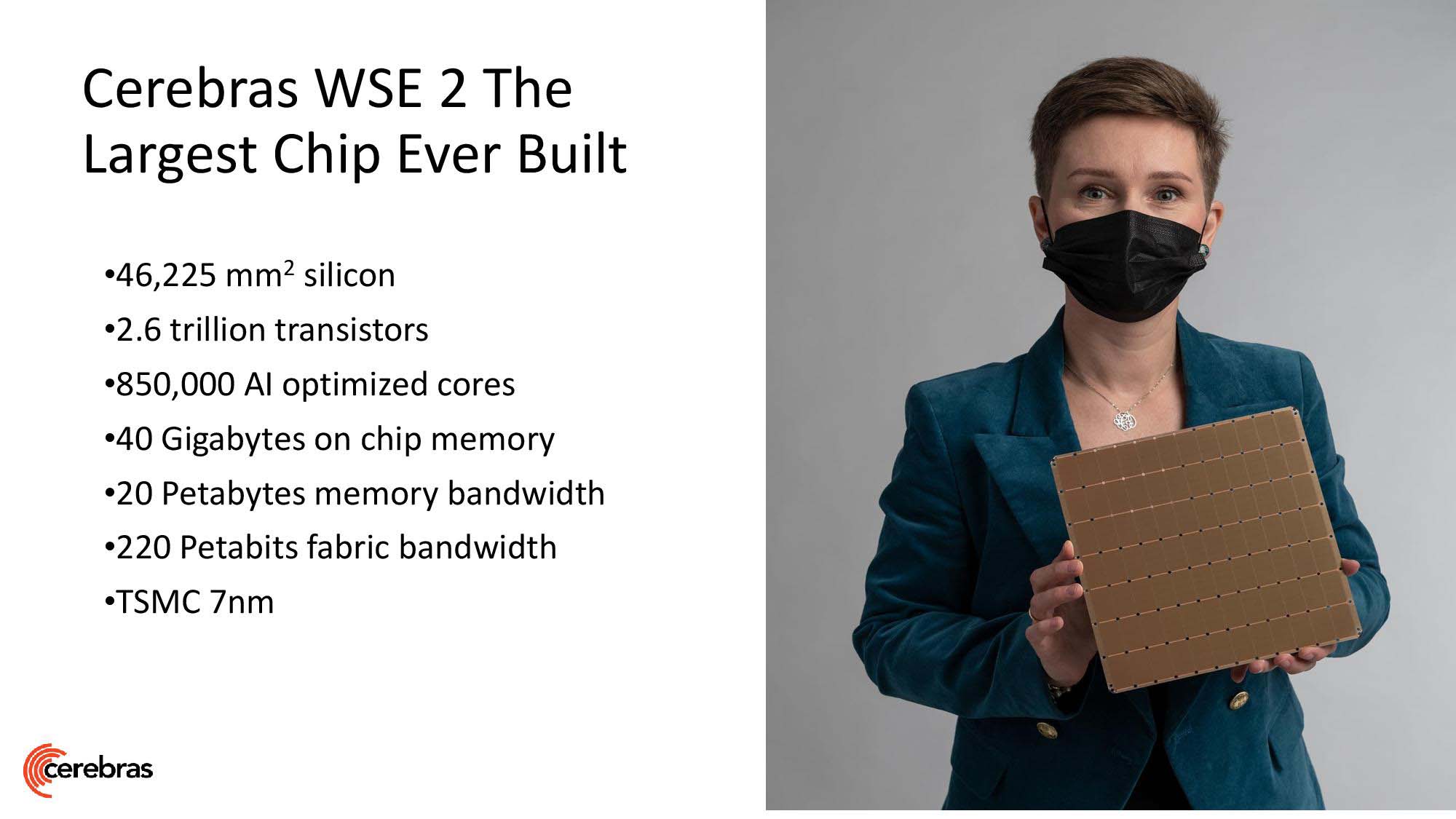
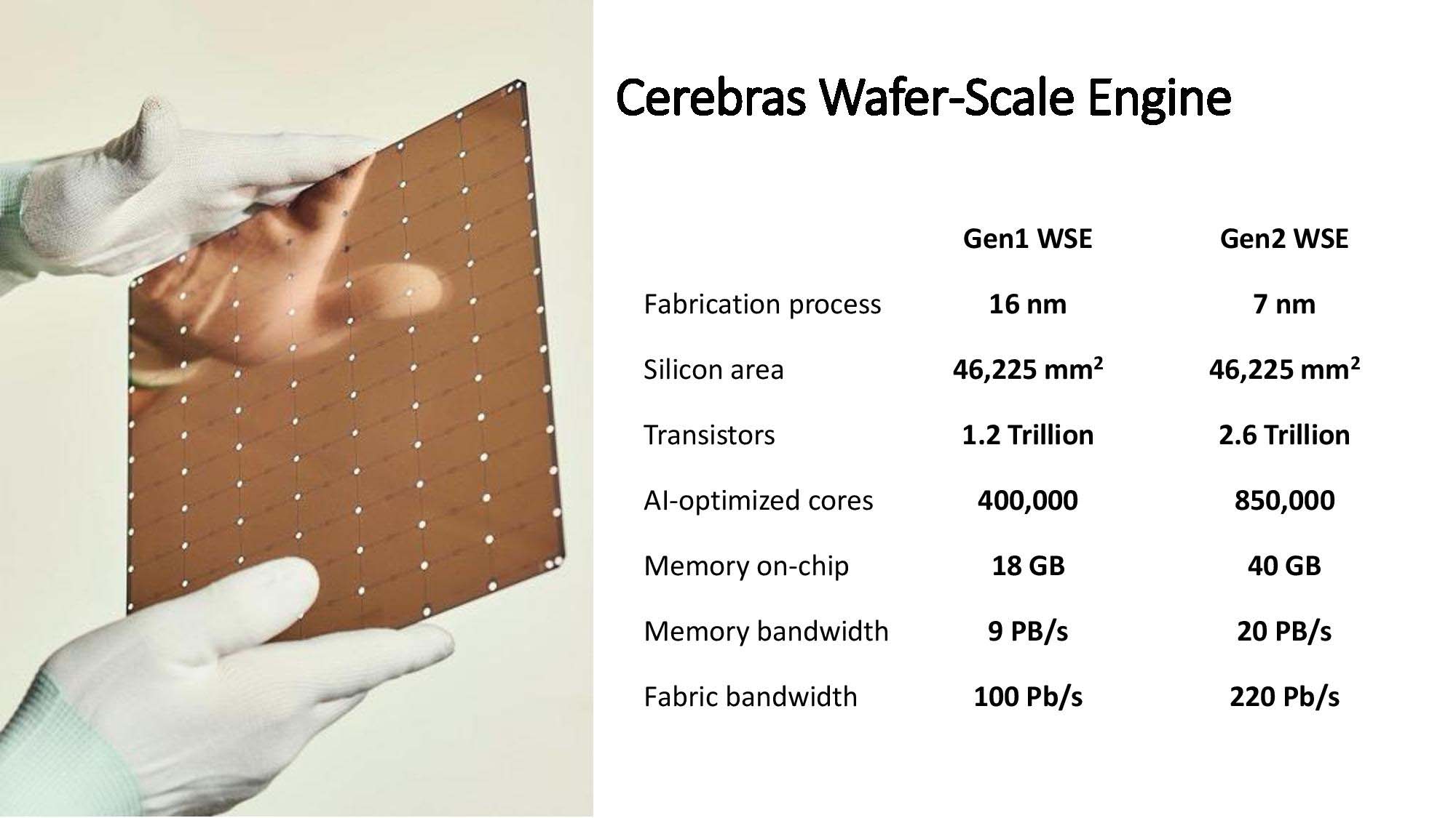
Decades of semiconductor design favored monolithic single chips until AMD showed the power of chiplets with its Zen architecture - essentially, AMD pioneered the mainstream use of smaller semiconductor "blocks" (in Zen, represented by the CCX, or Core Complex) that are then glued (as per Intel's own words) together into the final chip, interconnected by AMD's own Infinity Fabric (responsible for carrying information from one chiplet to another). This circumvents some limitations on currently available semiconductor manufacturing processes, since smaller chips are less likely to feature manufacturing defects, and allows chip designers to better spread out computing resources to achieve a better balance between transistor density and the heat generated by these closely packed-together components. Even as chiplets are gaining traction in the industry and are likely to become the new de-facto standard for performance scaling (Nvidia and Intel have also been exploring chiplets and MCM [Multi-Chip Modules] for future products), there are still some players looking into new ways of increasing chip performance density, such as Cerebras, with the 2.3 trillion transistors, 850,000 cores and 15 kW power requirement of its Wafer Scale Engine 2.
The Wafer Scale Engine is the world's largest chip, as you might have guessed from those eye-watering statistics, putting some supercomputers to shame by itself. The decision to go wafer-scale aimed to solve one of the problems arising from the deployment of larger and larger amounts of individual chips working in tandem - they have to communicate between each other, to know where information is, at what processing state the data is, and to transmit it towards the next processing step. Keeping everything in a single chip means that the distance between different ICs is shortened, and enabled Cerebras to develop their own interconnect technology (akin to AMD's Infinity Fabric) which enables transmission of data at up to 220 Petabits/S. However, Cerebras' Wafer Scale Engine is still a monolithic chip at heart, meaning that it still faces the same constraints as they do - particularly, a higher surface area for manufacturing defects to occur. While the company has built-in additional resources into the chips' design that aim to alleviate those issues - namely, additional cores and IC components that can substitute for those that have been disabled due to manufacturing defects - this still has to be considered when it comes to the future of computing. However, lessons learned from Cerebras' design are very likely to be carried over to future wafer-sized computing solutions.
Article continues below


One such solution presents a perfect theoretical marriage between both wafer-scale designs and the more cost-effective chiplet approach - a chiplet-based, wafer-scale chip. The idea is simple: take the basis of Cerebras' innovation - a wafer-sized substrate that enables an interconnect fabric between all components - and instead of carving a monolithic chip from that, you "simply" add chiplet-based blocks on top of the interconnect. I say simply, because the work of bonding a number of ICs on a substrate is much more complex than it sounds. Even so, this would allow a prospective chip designer to leverage and combine multiple, perhaps even disparate silicon blocks into the wafer-sized chip, thus improving yields and overall chip cost. Imagine an AMD-made wafer-scale engine that combined multiple Zen 3 CCX's as well as graphics chips, Xilinx-based FPGAs, Arm cores, and whatever else comes to your mind - just deployed on a wafer-sized substrate.
This actually coincides with the thought-process taken the first time a wafer-scale chip was discussed among the scientific community, authored by Saptadeep Pal and colleagues; the design of a wafer-scale chip based on heterogeneous computing philosophies. And even as powerful as Cerebras' Wafer Scale Engine is, it is already going up against the neverending pit of compute power requirements around the globe. Rakesh Kumar, a University of Illinois collaborator on the waferscale effort with Pal, described the entire heterogeneous wafer-scale design as such: ”A chiplet-based approach allows heterogeneous integration of technologies on the wafer. This means that a chiplet-based waferscale processor can have high density memories such as DRAMs, flash, etc., reside on the same processor. This can allow much better memory capacity characteristics than the Cerebras approach that cannot support heterogeneous technologies on the processor, limiting the processor’s memory capacity. This is going to be critical for many applications (including many ML models) whose application requirements far exceed what is provided by the Cerebras processor."
The best part? Such a design can already be achieved with today's technology. It seems like it's only a matter of time before Moore's Law is proven yet again.
Get Tom's Hardware's best news and in-depth reviews, straight to your inbox.

Francisco Pires is a freelance news writer for Tom's Hardware with a soft side for quantum computing.
-
I hate that whole Moore’s law thing it isn’t a law it was an observation there’s no law to it!!! Other things in physics are laws, like the speed of light that’s a law—not some dumb observation It was only true for a brief period of timeReply
If Moore’s law was a law then it would still be in effect and working and we wouldn’t have run into a wall so stop calling it a law it was a comment made by a old dude who made an observation
Leave it to Intel to make Observations and call them a law. So puffed with pride they were. It’s another reason that I detest them and I don’t care for their lackluster hardware at all. None of it -
gargoylenest Reply
Good observation :unsure:Mandark said:I hate that whole Moore’s law thing it isn’t a law it was an observation there’s no law to it!!! Other things in physics are laws, like the speed of light that’s a law—not some dumb observation It was only true for a brief period of time
If Moore’s law was a law then it would still be in effect and working and we wouldn’t have run into a wall so stop calling it a law it was a comment made by a old dude who made an observation
Leave it to Intel to make Observations and call them a law. So puffed with pride they were. It’s another reason that I detest them and I don’t care for their lackluster hardware at all. None of it