


Cerebras, the company behind the Wafer Scale Engine (WSE), the world's largest single processor, shared more details about its latest WSE-2 today at the Linley Spring Processor Conference. The new WSE-2 is a 7nm update to the original Cerebras chip and is designed to tackle AI workloads with 850,000 cores at its disposal. Cerebras claims that this chip, which comes in an incredibly small 26-inch tall unit, replaces clusters of hundreds or even thousands of GPUs spread across dozens of server racks that use hundreds of kilowatts of power.
The new WSE-2 now wields 850,000 AI-optimized cores spread out over 46,225 mm2 of silicon packed with 2.6 trillion transistors. Cerebras also revealed today that the second-gen chip has 40 GB of on-chip SRAM memory, 20 petabytes of memory bandwidth, and 220 petabits of aggregate fabric bandwidth. The company also revealed that the chip consumes the same 15kW of power as its predecessor but provides twice the performance, which is the benefit of moving to the denser 7nm node from the 16nm used with the previous-gen chip.
Cerebras Wafer Scale Engine 2 WSE-2 Specifications
| Row 0 - Cell 0 | Cerebras Wafer Scale Engine 2 | Cerebras Wafer Scale Engine | Nvidia A100 |
| Process Node | TSMC 7nm | TSMC 16nm | TSMC 7nm N7 |
| AI Cores | 850,000 | 400,000 | 6,912 + 432 |
| Die Size | 46,255 mm2 | 46,255 mm2 | 826 mm2 |
| Transistors | 2.6 Trillion | 1.2 Trillion | 54 Billion |
| On-Chip SRAM Memory | 40 GB | 18 GB | 40 MB |
| Memory Bandwidth | 20 PB/s | 9 PB/s | 1,555 GB/s |
| Fabric Bandwidth | 220 Pb/s | 100 Pb/s | 600 GB/s |
| Power Consumption (System/Chip) | 20kW / 15kW | 20kW / 15kW | 250W (PCIe) / 400W (SXM) |
These almost unbelievable specifications stem from the fact that the company uses an entire TSMC 7nm wafer to construct one large chip, thus sidestepping the typical reticle limitations of modern chip manufacturing to create a wafer-sized processor. The company builds in redundant cores directly into the hardware, which then leaves room for disabling defective cores, to sidestep the impact of defects during the manufacturing process.
The company accomplishes this feat by stitching together the dies on the wafer with a communication fabric, thus allowing it to work as one large cohesive unit. This fabric provides 220 Petabits/S of throughput for the WSE2, which is slightly more than twice the 100 Petabits/S of the first-gen model. The wafer also includes 40GB of on-chip memory that provides up to 20 Petabytes/S of throughput, both of which are also more than twice that of the previous-gen WSE.


Cerebras hasn't specified the WSE-2's clock speeds, but has told us in the past that the first-gen WSE doesn't run at a very "aggressive" clock (which the company defined as a range from 2.5GHz to 3GHz). We're now told that the WSE-2 runs at the same clock speeds as the first-gen model, but provides twice the performance within the same power envelope due to its increased system resources. We certainly don't see those types of generational performance improvements with CPUs, GPUs, or most accelerators. Cerebras says that it has made unspecified changes to the microarchitecture to extract more performance, too.
As you can see below, cores are distributed into tiles, with each tile having its own router, SRAM memory, FMAC datapath, and tensor control. All cores are connected via a 2D mesh low-latency fabric. The company claims these optimizations result in a 2x improvement in wall clock training time with a BERT-style network training that was completed using the same code and compiler used with the first-gen wafer-scale chip.


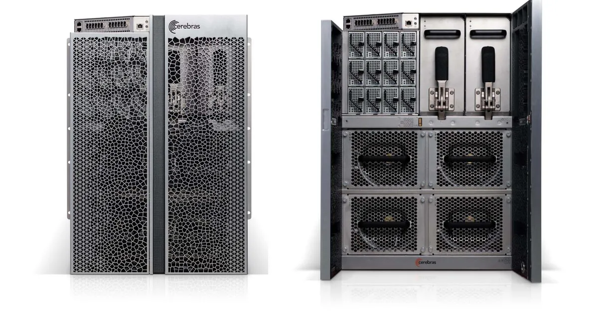
As before, the chip comes wrapped in a specialized 15U system that's designed specifically to accommodate the unique characteristics of the wafer-scale device. We're told that the changes to the first-gen CS-1 system, which you can read about in-depth here, are very minimal in the new CS-2 variant. Given that the most important metrics, like power consumption and the size of the WSE, have remained the same, it makes sense that most of the system is identical.
Cerebras hasn't specified pricing, but we expect the WSE-2 unit will continue to attract attention from the military and intelligence communities for any multitude of purposes, including nuclear modeling, but Cerebras can't divulge several of its customers (for obvious reasons). It's safe to assume they are the types with nearly unlimited budgets, so pricing isn't a concern. On the public-facing side, the Argonne National Laboratory is using the first systems for cancer research and basic science, like studying black holes.
Cerebras also notes that its compiler easily scaled to exploit twice the computational power, so the software ecosystem that is already in place is supported. As such, the WSE-2 unit can accept standard PyTorch and TensorFlow code that is easily modified with the company's software tools and APIs. The company also allows customers instruction-level access to the silicon, which stands in contrast to GPU vendors.
Cerebras has working systems already in service now, and general availability of the WSE-2 is slated for the third quarter of 2021.
