
Cerebras Systems' announced its new CS-1 system here at Supercomputing 2019. The company unveiled its Wafer Scale Engine (WSE) at Hot Chips earlier this year, and the chip is almost as impressive as it is unbelievable: The world's largest chip, weighing in at an unbelievable 400,000 cores, 1.2 trillion transistors, 46,225 square millimeters of silicon, and 18 GB of on-chip memory, all in one chip that is as large as an entire wafer. Add in that the chip sucks 15kW of power and features 9 PB/s of memory bandwidth, and you've got a recipe for what is unquestionably the world's fastest AI processor.
Developing the chip was an incredibly complex task, but feeding all that compute enough power, not to mention enough cooling capacity, in a system reasonable enough for mass deployments is another matter entirely. Cerebras has pulled off that feat, and today the company unveiled the system and announced that the Argonne National Laboratory has already adopted it. The company also provided us detailed schematics of the internals of the system.

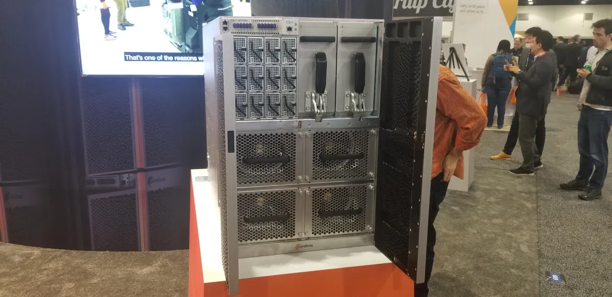


The system measures a mere 15 Rack Units tall, or roughly 26", so three can fit in a single rack. Given the performance, that's an incredibly compact package: It would take a 1,000-GPU cluster, which consumes 15 entire racks and half a megawatt of power, to match the performance of one CS-1 system. That's because a single Cerebras chip has 78 times more cores, 3,000 times more memory, and 10,000 times more memory bandwidth than a single GPU. It also has 33,000 times more bandwidth (PB/s).

A pod of Google's TPU v3 chips consumes 100kW of power, but only provides 1/3 the performance of a single CS-1 system. Overall, the CS-1 draws 1/5th the power and is 1/30th the size, yet is three times faster than an entire TPU pod.


In contrast, the Cerebras CS-1 consumes 20kW, with 4kW of power dedicated to the cooling subsystem, like fans, pumps, and the heat exchanger. The system delivers 15kW of power to the chip, and the remaining 1kW is lost to power supply inefficiencies.
Twelve 100GbE connections line the upper left corner of the system. These systems will work in tandem with larger supercomputers that execute traditional forms of compute. Data processed by a supercomputer will then flow into the CS-1 for additional AI processing, leveraging the strengths of the both types of compute for differing workloads. The system also scales out to numerous nodes via the networking fabric, meaning the CS-1 systems can work in larger groups. Cerebras has tested 'very large' clusters, which can then be managed as a single homogeneous system in model parallel of data parallel modes, but hasn't released official scalability metrics.
The entire Cerebras CS-1 consists of custom-built components. The system takes in power from the rear with twelve power connections. It then steps 54V down to 0.8V before delivering it to the chip. The power flows through the motherboard, as opposed to around it, and then into the processor, with separate regions of an unspecified number of cores each receiving their own supply of power. The wafer-scale chip consists of many die tied together with an on-die networking fabric, but we're told that the power delivery is more granular than a die/reticle flash. That ensures consistent delivery of power across the wafer, and also minimizes on-chip power distribution planes.


The "engine block" sits up front. This is a sandwiched design that has the power subsystem, motherboard, chip, and cold plate mounted as one assembly (left). The cold plate receives water from a manifold to the right, which then delivers cooled water to several individual zones on the surface of the cooling plate. The heated water is then extracted, again from the small zones that ensure consistent thermal dissipation, and pumped down to the heat exchanger at the bottom of the unit. The exchanger consists of an EMI grill and is cooled by powerful fans that employ air straighteners. Overall, the chip runs at half the junction temperature of a standard GPU, which increases reliability.
All of the individual units, like the 6+6 power supplies, heat pumps, fans, and heat exchanger, are redundant and hot-swappable to minimize downtime and failures.
The chip is fabbed on TSMC's 16nm process, which the company chose due to its maturity and the scheduling of its product release. Cerebras hasn't specified the clock speeds, but tells us the chip doesn't run at a very "aggressive" clock (which the company defined as a range from 2.5GHz to 3GHz). The company will provide specifics in the near future.


Cerebras hasn't specified pricing for the unit, though we're told it is "several million." We expect that this unit will attract attention from the military and intelligence communities for any multitude of purposes, including nuclear modeling, but Cerebras can't divulge several of its customers (for obvious reasons). It's safe to assume they are the types with nearly unlimited budgets, so pricing isn't a concern.
On the public-facing side, the Argonne National Laboratory is using the first systems for cancer research and basic science, like studying black holes. Cerebras has a software ecosystem already in place, and the unit can accept standard PyTorch and TensorFlow code that is easily modified with the company's software tools and APIs. The company also allows customers instruction-level access to the silicon, which stands in contrast to GPU vendors.
