AMD deep-dives Zen 5 architecture — Ryzen 9000 and AI 300 benchmarks, RDNA 3.5 GPU, XDNA 2, and more
Zen 5's 16% IPC improvement floats all boats.
AMD Zen 5 Microarchitecture
| (up to values) | Zen 5 (2024) | Zen 4 (2022) | Zen 3 (2020) | Zen 2 (2019) | Zen 1 (2017) |
| IPC Increase (AMD) | +16% | +13% | +19% | +15% | +52% |
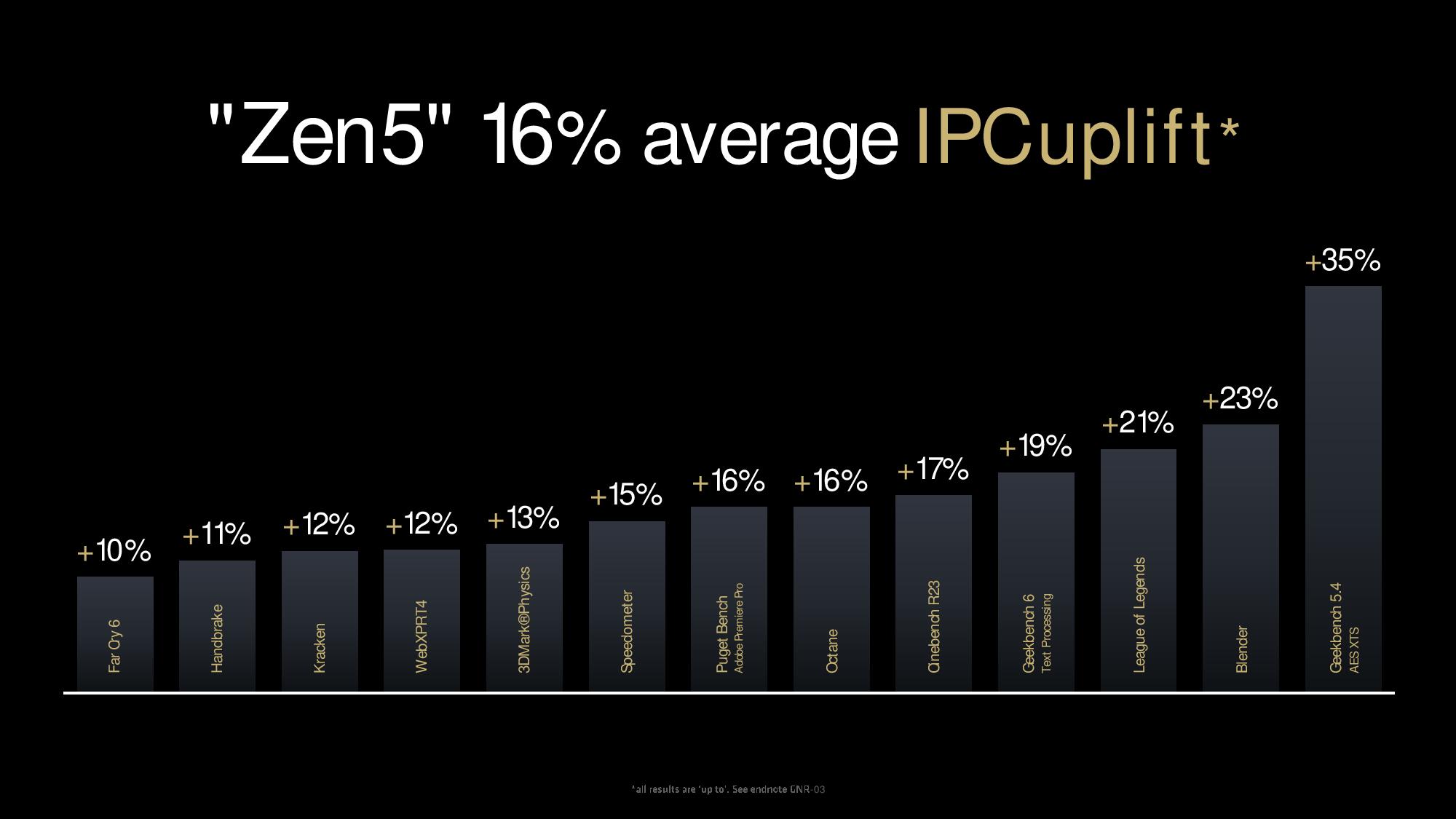
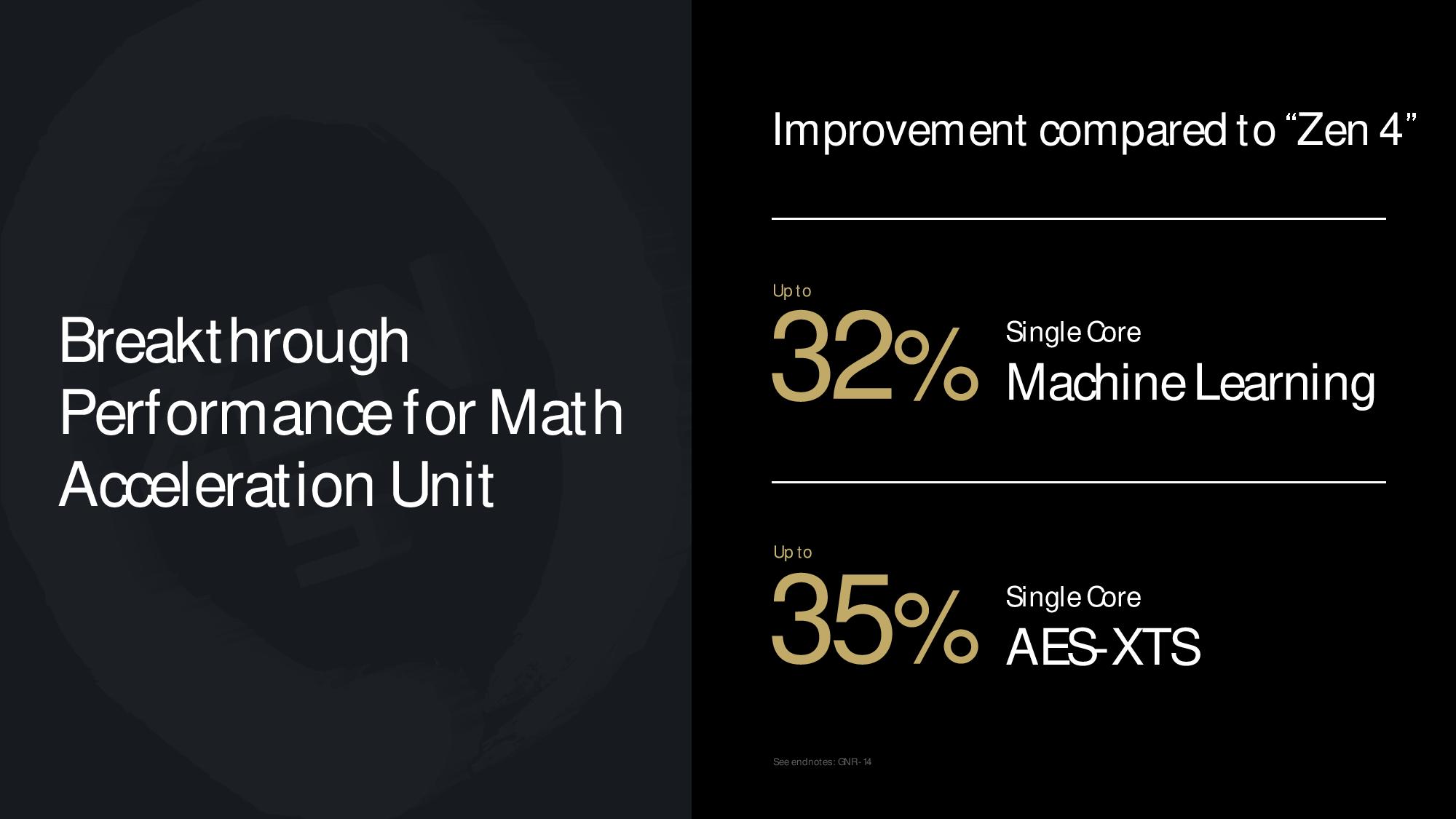
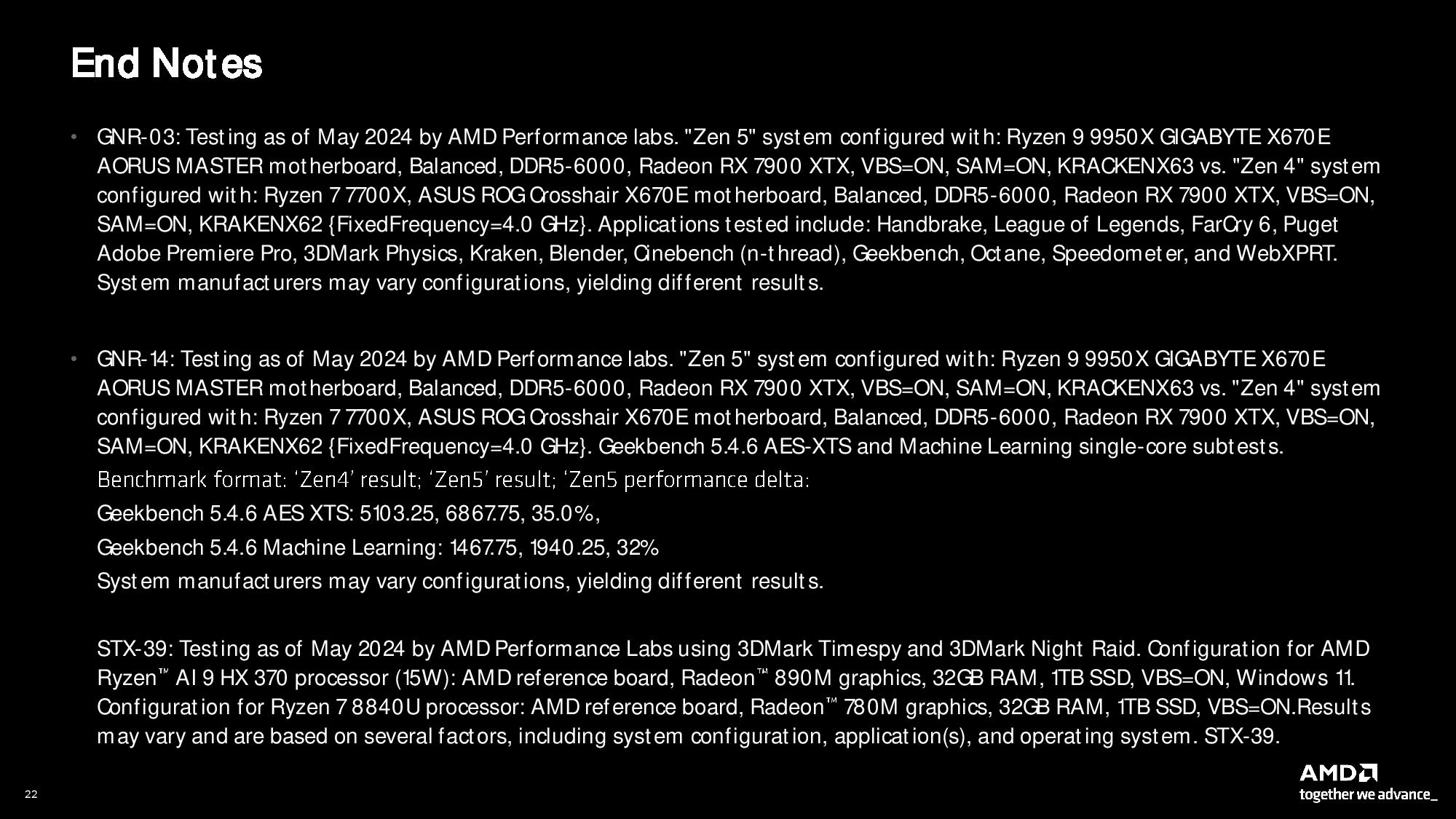
The Zen architecture debuted with a 52% IPC improvement over Bulldozer in 2017, and the company has delivered double-digit IPC increases in every generation since. Zen 5 has a 16% increase in IPC, as measured across 13 workloads. Zen 5 has dramatically improved vector math performance, with a 32% gain over Zen 4 in single-core machine learning (VNNI) and a 35% gain in single-core AES-XTS encryption workloads (AVX-512), as measured by the Geekbench subtests.
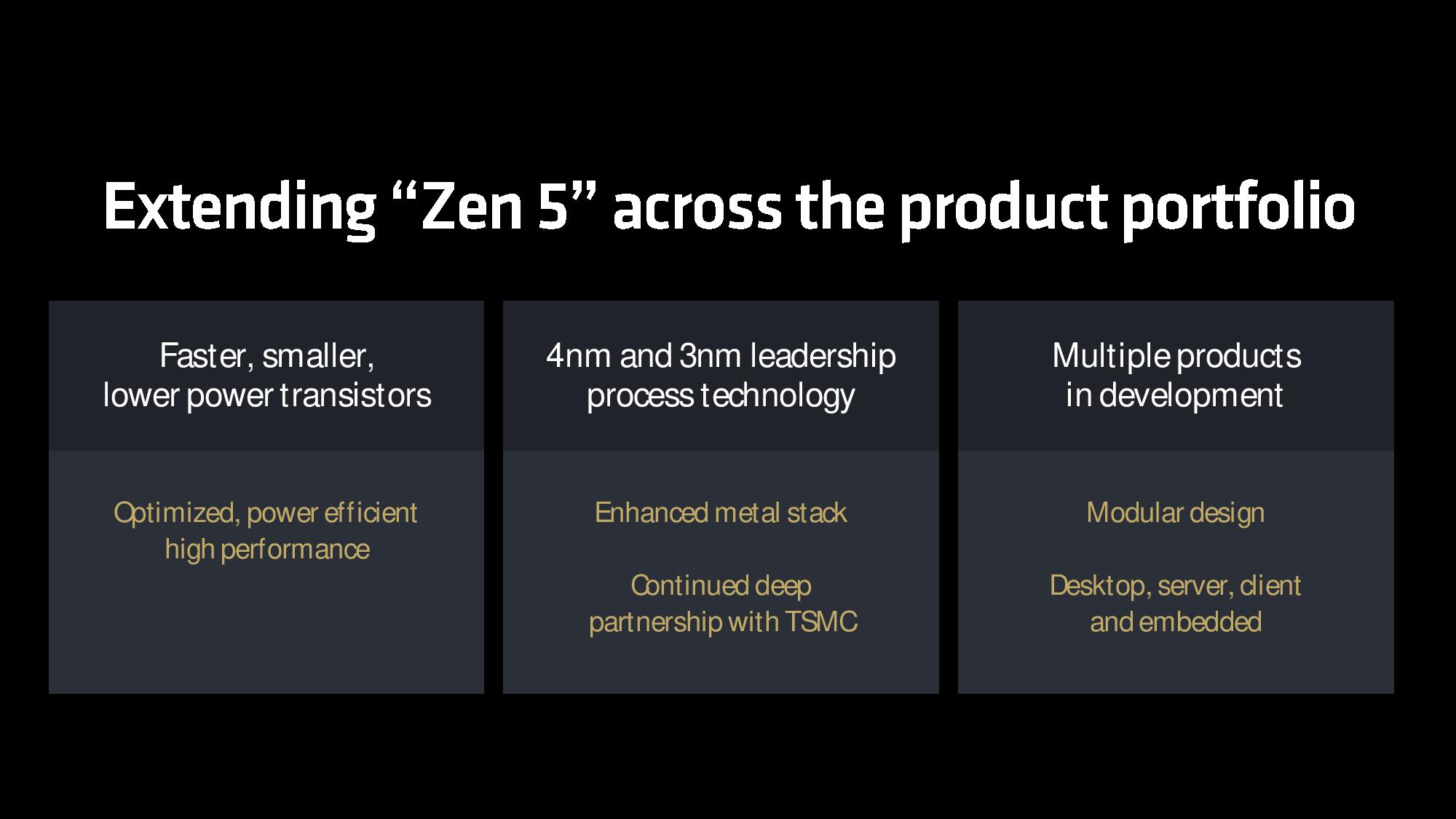
Zen 5 is an overhaul with new architectural underpinnings that its lead architect, Mike Clark, says will serve as the foundation for the next several generations of microarchitectures. It will also be used for chips with the TSMC 4nm and 3nm process nodes, with concurrent leapfrogging teams working on both designs.
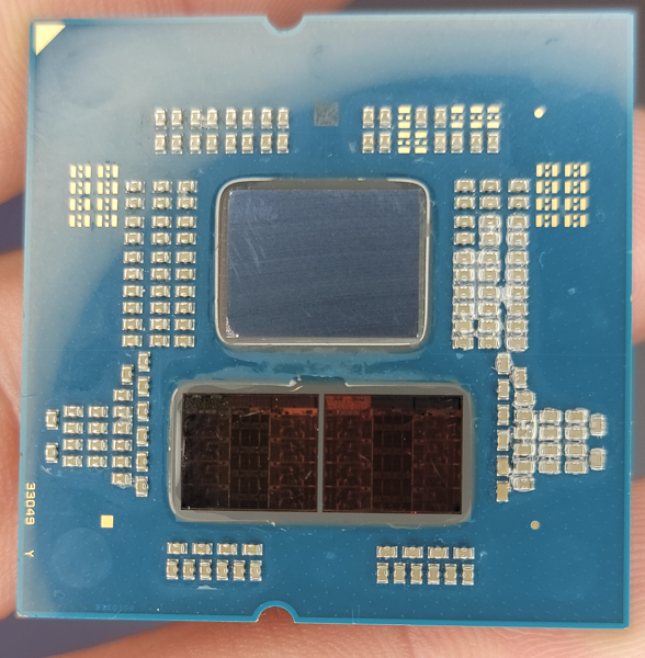
As with Zen 4 processors, the core compute die (CCD) has a maximum of eight cores and a large central 32MB shared L3 complex. Two CCDs are connected to the same 6nm I/O Die (IOD) used with the Zen 4 processors, so the chip provides the same graphics support and basic connectivity options. You can see the Ryzen 9000 diagram in the second image above.
AMD didn’t share any new slides about the compact Zen 5c cores, but we teased out a few details. As a reminder, AMD's Zen 5c cores are designed to consume less space on a die than the 'standard' Zen 5 performance cores while delivering enough performance for less demanding tasks, thus saving power and delivering more compute horsepower per square millimeter than was previously possible (deep dive here).
Intel's E-Cores take a similar approach, but AMD’s Zen 5c employs the same microarchitecture as the standard Zen 5 cores and supports the same features with its smaller cores. In contrast, Intel’s design employs different architectures and feature support for each core type. The smaller Zen 5c cores operate at lower clock rates and provide less peak performance than standard cores, but they also preserve die area for other elements, like a larger GPU and NPU.
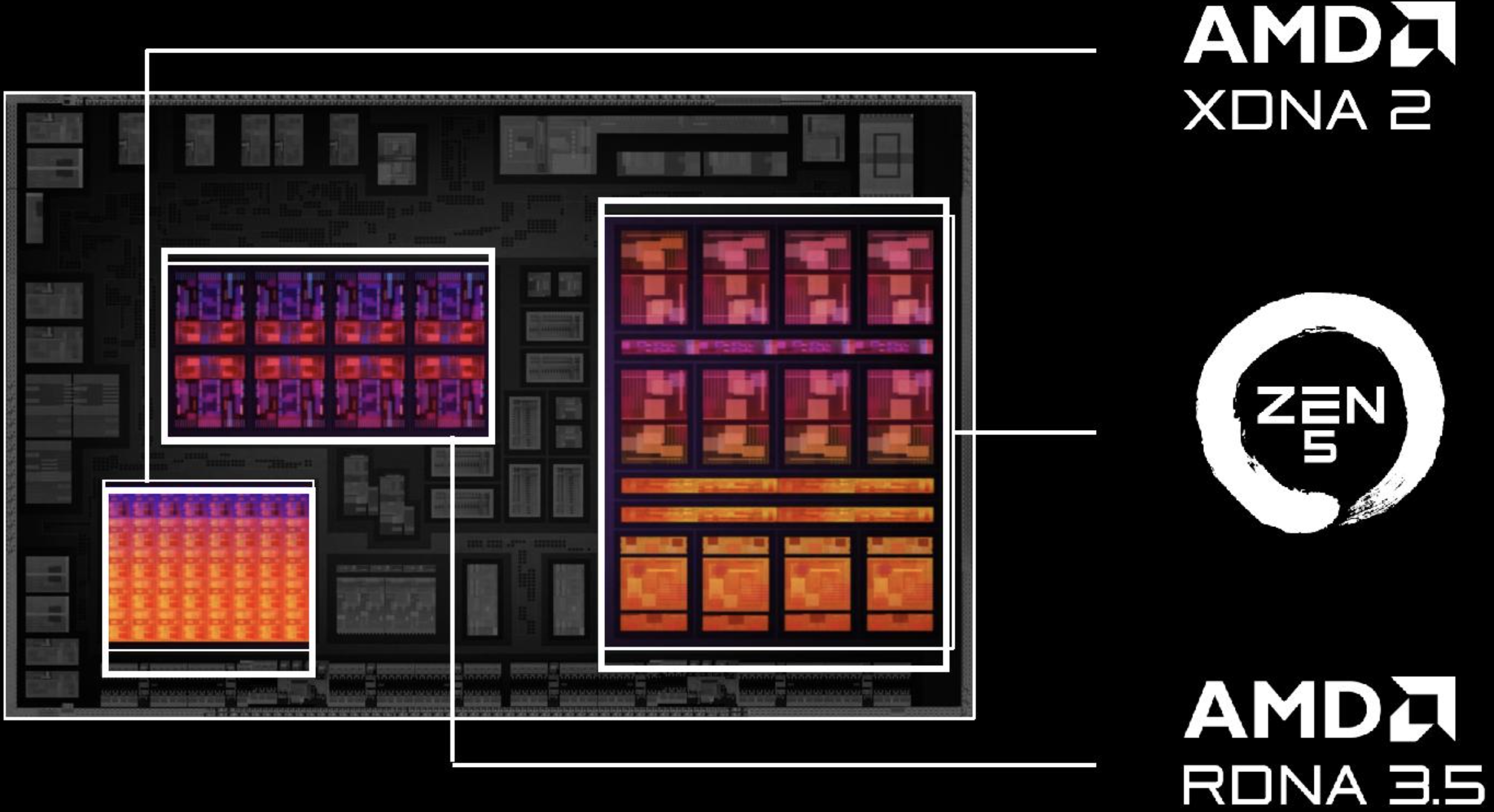
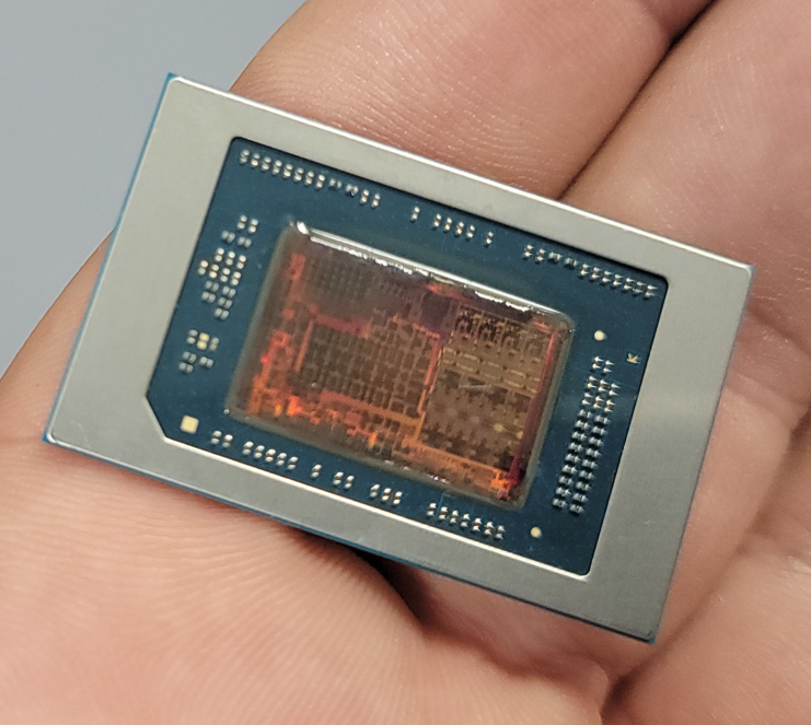
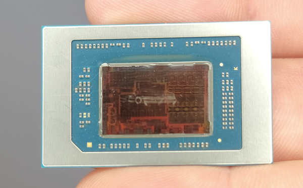
Above, you can see the previously shared image that shows the floorplan for the Ryzen AI 300 processors and the following image of the die, which has been sanded down to reveal the architecture underneath the cover. This shows the architecture in surprising detail. The four standard Zen 4 cores are aligned at the bottom of the Zen 5 cluster of cores, and the eight Zen 5C cores are aligned at the top.
Both core types have their own private L1 and L2 caches, but the 24MB of L3 cache is split into an 8MB slice for the standard cores and a 16MB slice for the Zen 5c compact cores (this can be seen as a single line running down the center of the eight Zen 5C cores in the block diagram).
As such, these two L3 caches have to communicate with each other over the data fabric, much like the CCX-to-CCX cache coherency mechanism found with AMD’s older Zen 2 architecture. This does introduce higher latency for cache-to-cache transfers, which AMD says is “not any more than you would have to go to memory for.” As such, AMD uses Windows scheduler mechanisms to attempt to constrain workloads to either the Zen 5 or 5C cores to reduce the occurrence of high latency transfers, with background workloads typically being assigned to the 5C cores. AMD will study behavior in the real world with concurrent apps running on both types of cores, thus continually assessing whether it would make sense to unify the L3 cache in future designs.
The design ties the three compute engines — CPU, NPU, and GPU — together with a data fabric. Each of the CPU clusters (Zen 5 and 5C) has a 32B/cycle interface, while the GPU has four 32B/cycle interfaces into the data fabric, and the XDNA engine has a single 32B/cycle interface.
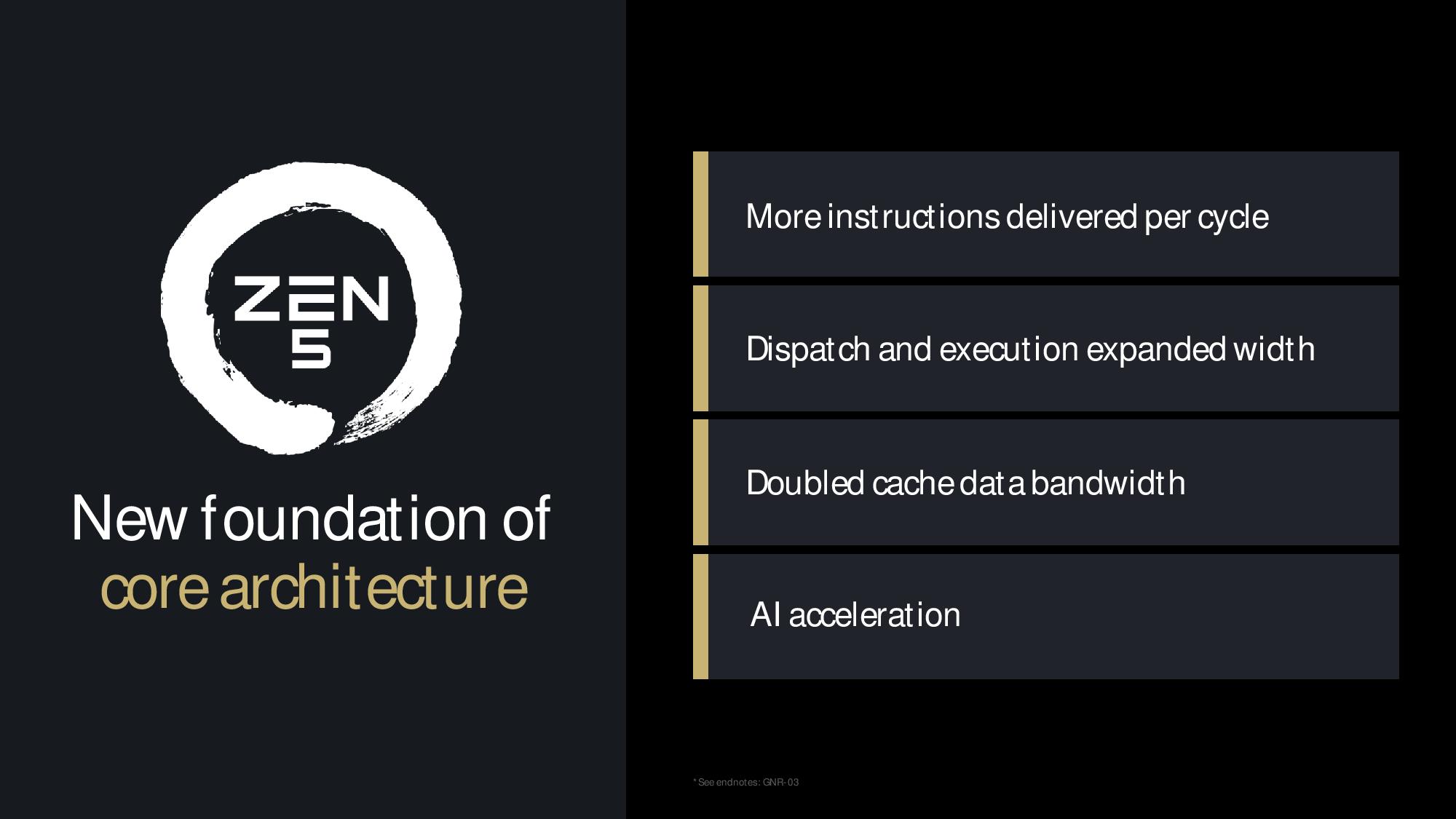
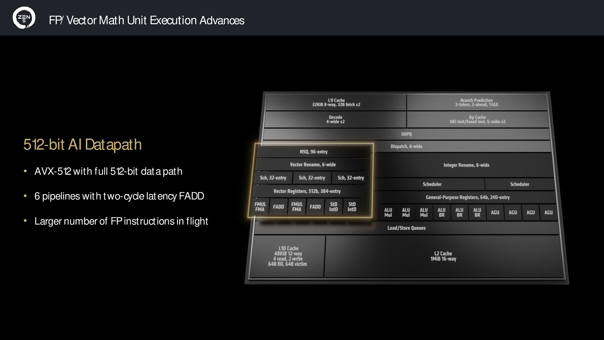
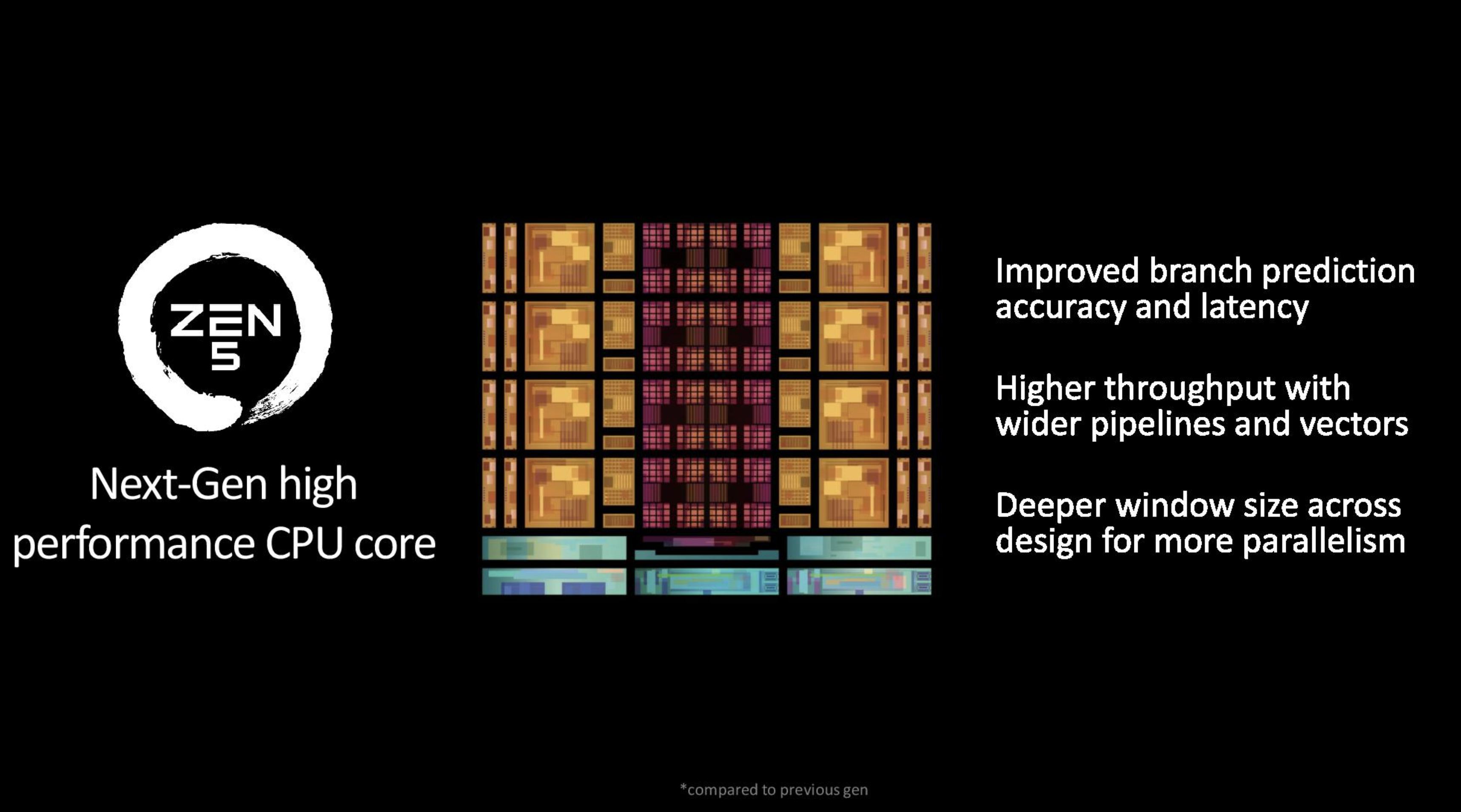
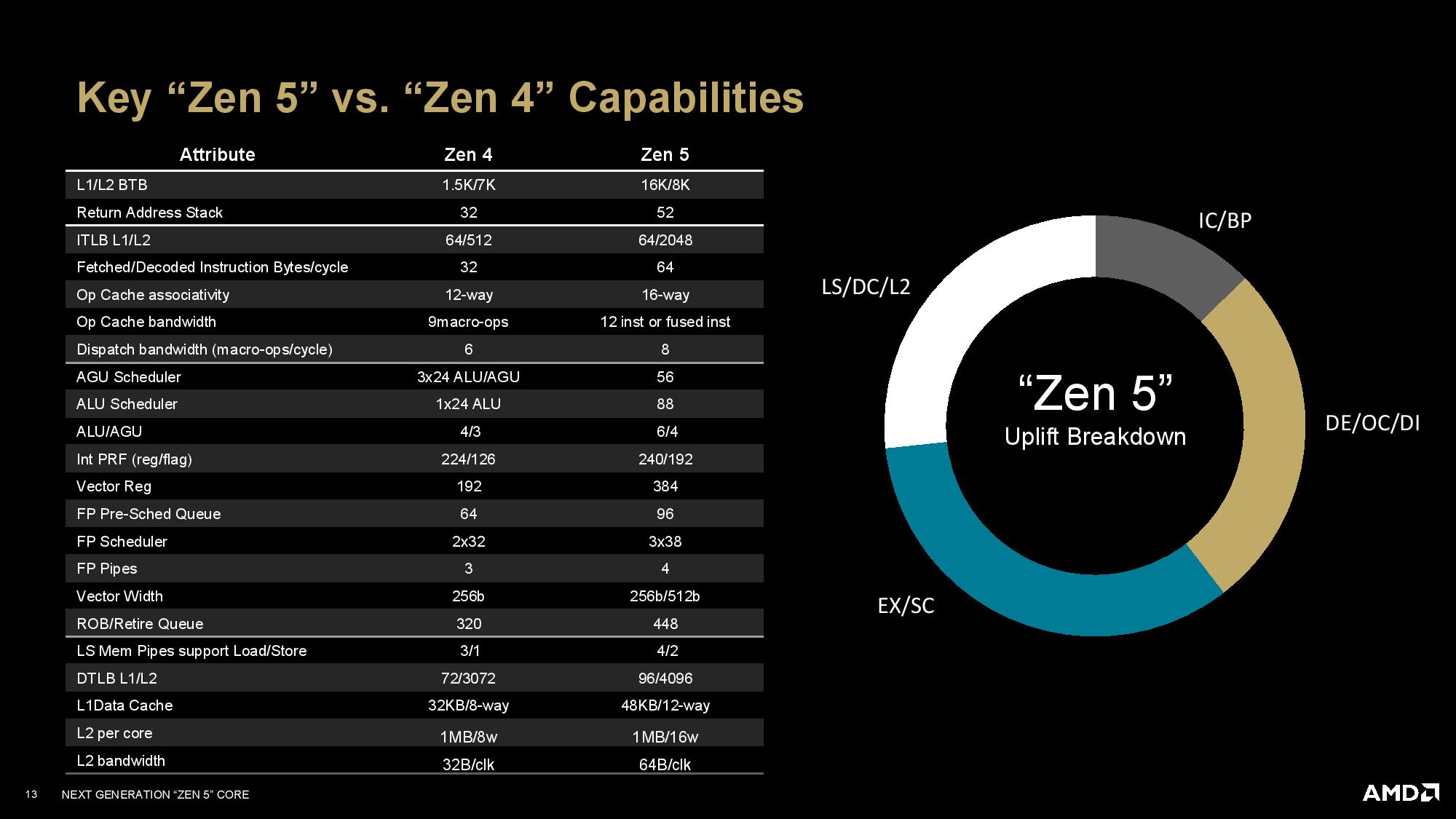
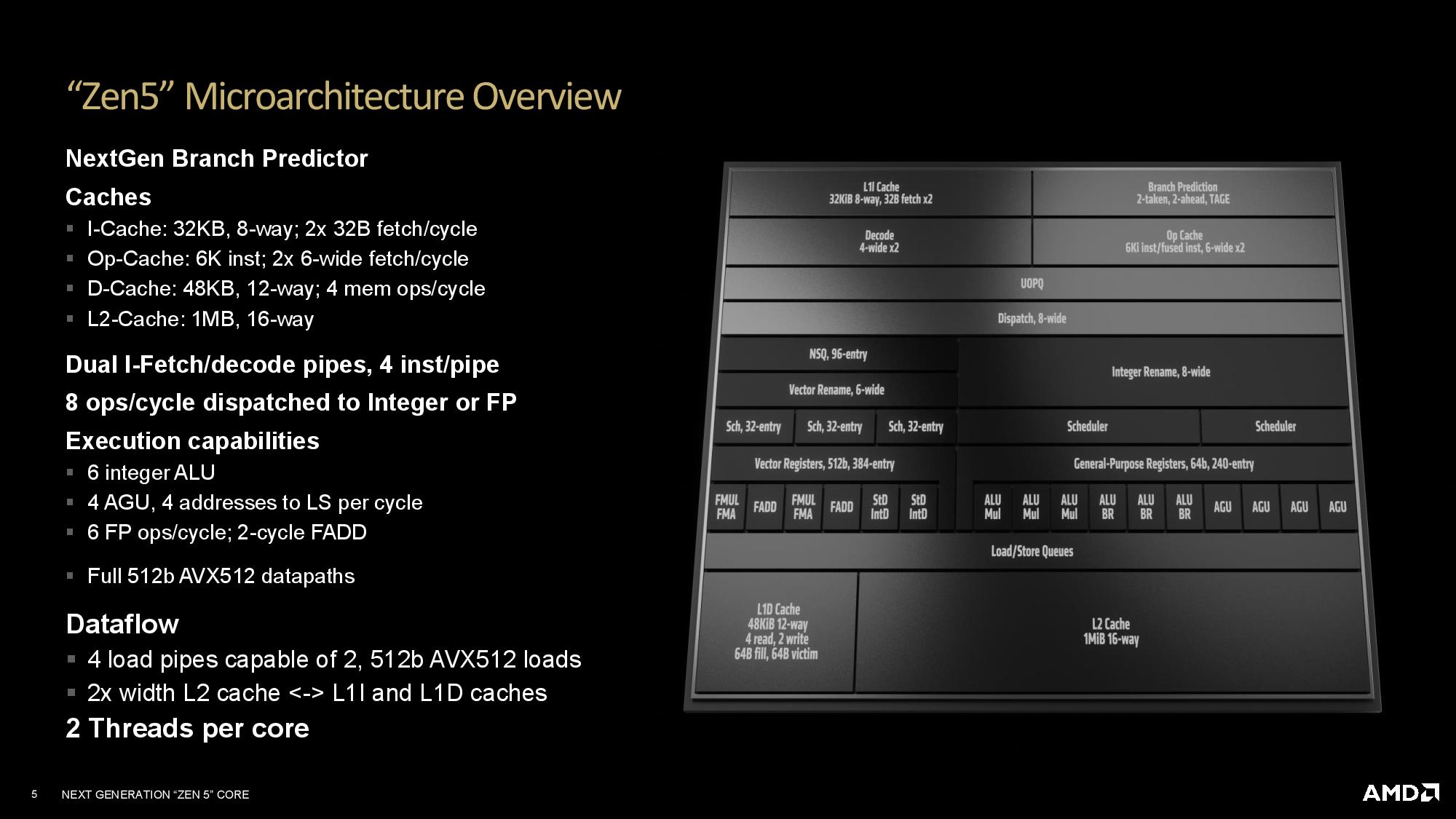
AMD redesigned the front end of the design with improved fetch, decode, and dispatch elements to feed a wider execution engine. It also doubled the data bandwidth between its L2 and L1 caches and the L1 to floating point unit, which it says helps deliver the generational gaming performance improvements.
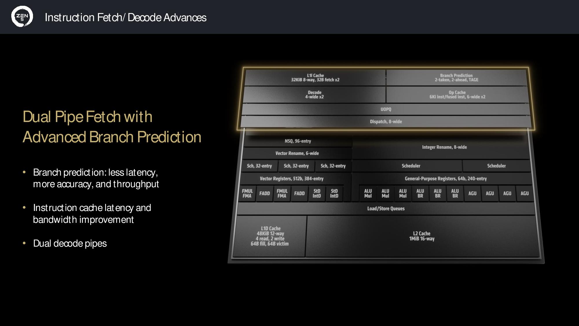
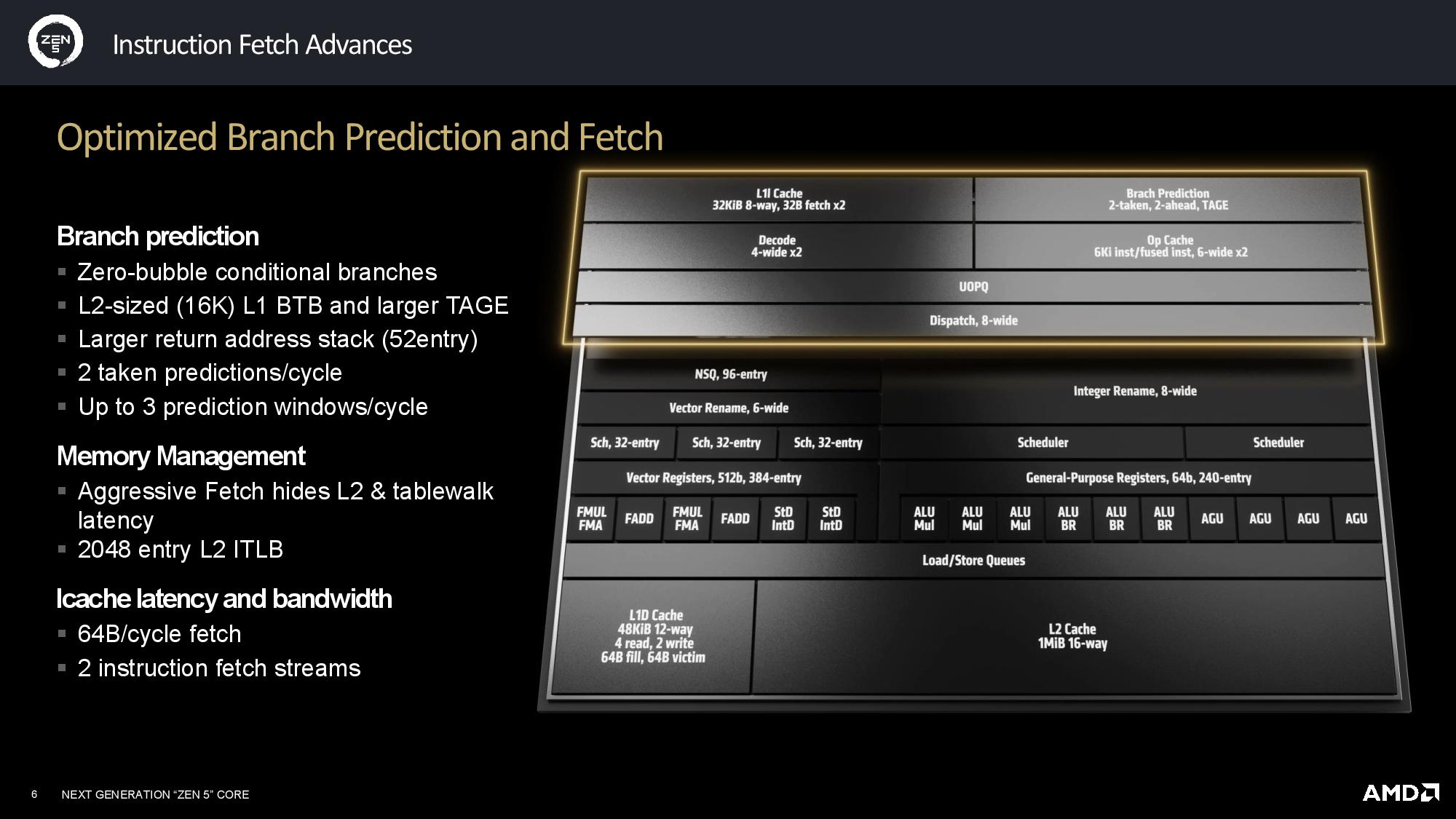
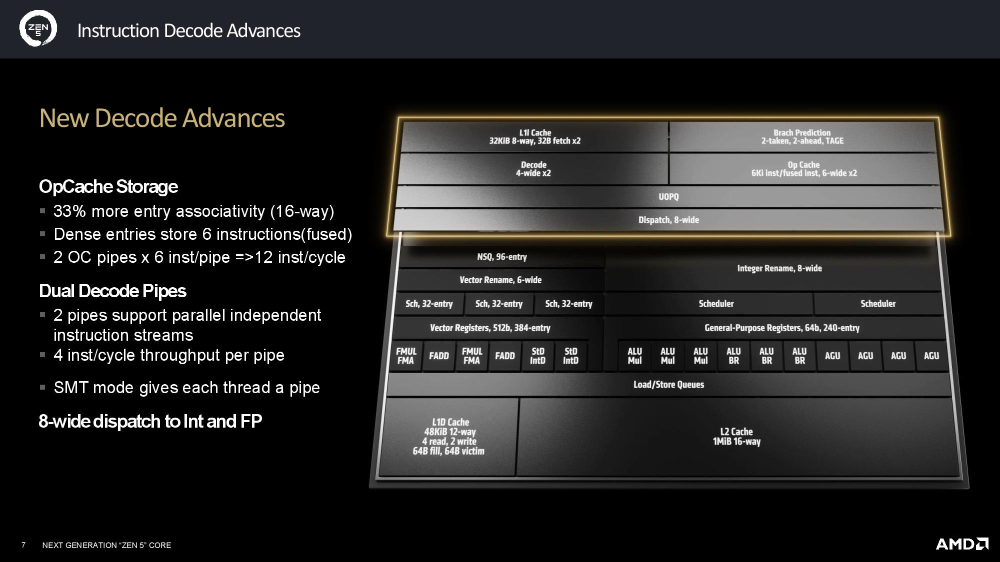
The front end features a dual pipe fetch and improved branch prediction accuracy that fuels feeding more predictions per cycle (TAGE branch prediction engine). Those predictions are fed into what are now dual-ported instruction and operation caches, which reduces latency. AMD also added a dual 4-wide decode path that feeds the micro-op queue, then the eight-wide dispatch.
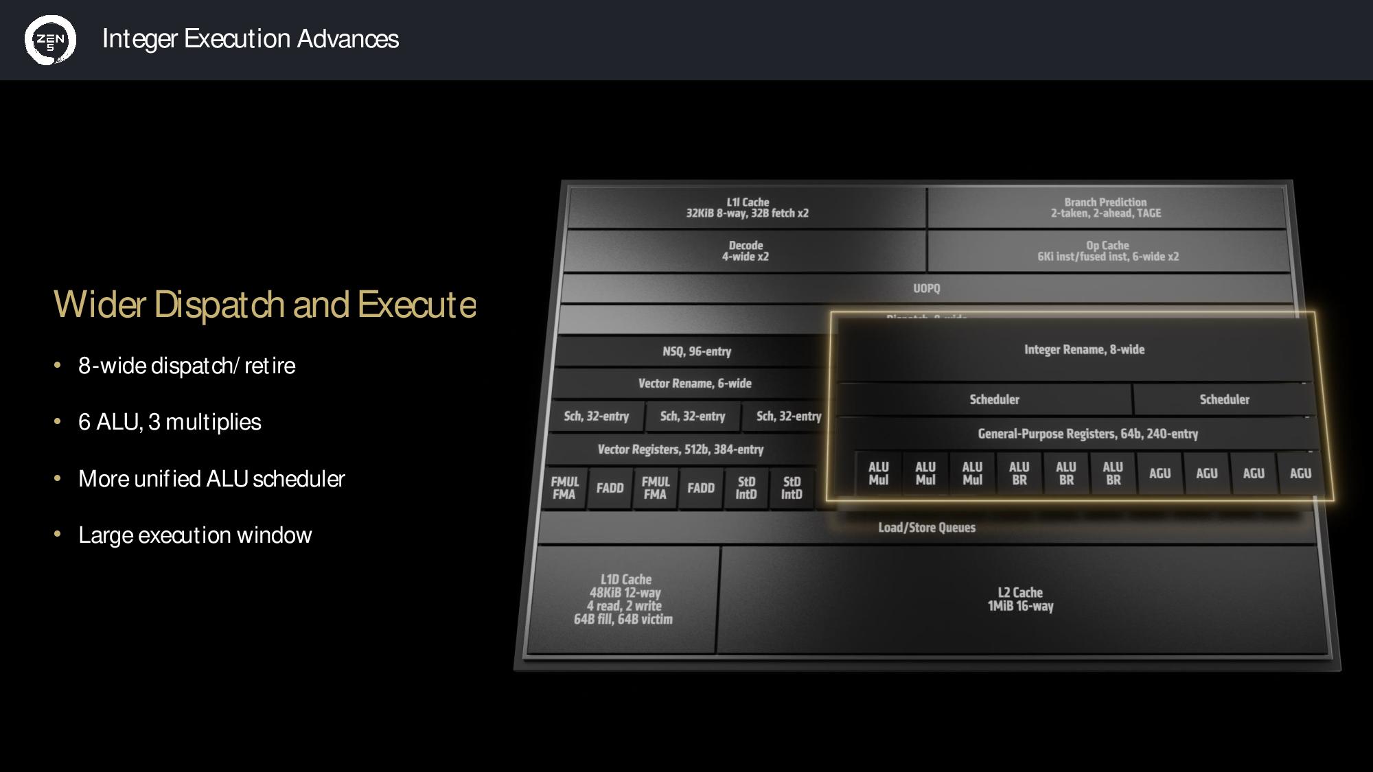
The Zen execution engine has long supported up to six instructions per cycle and four Arithmetic Logic Units (ALUs) for integer execution. Zen 5 marks the first time AMD has widened the Zen execution engine to support dispatching and retiring up to eight instructions per cycle, thus satisfying the increased instruction throughput from the front end.
Zen 4 had four schedulers for the integer unit, but Zen 5 has a unified ALU scheduler for all six ALU units. The execution window has also been widened by 40% (up to 448 outstanding ops) to better handle the extra misses that are a natural byproduct of the wider dispatch and execution.
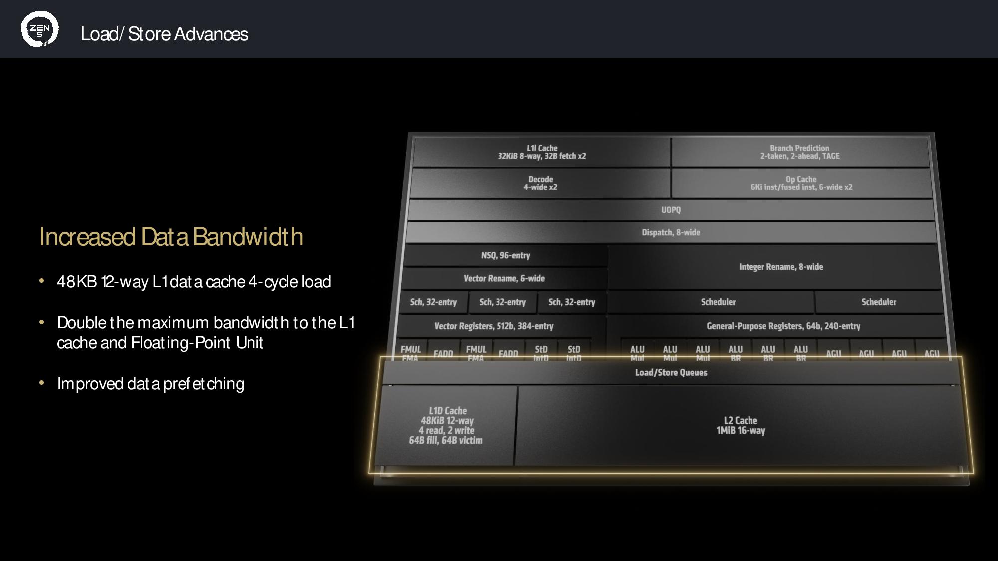
Zen 4 had a 32KB data cache, which has now been expanded to a 48KB 12-way L1 data cache (L1D) for Zen 5. Despite the increased capacity of the L1D, the unit maintains its 4-cycle load latency. Doubled bandwidth to the L1 cache and floating point unit is a crucial accommodation for the expanded AVX engine, which now supports a full 512-bit path.
Get Tom's Hardware's best news and in-depth reviews, straight to your inbox.
Zen 4 used a dual-issue AVX-512 pipeline (“double-pumped” in AMD parlance), wherein it essentially issued an AVX-256 instruction twice across a 256-bit interface to provide most of the performance benefits of AVX-512 while avoiding the impact to die area and resulting frequency drops.
Zen 5 supports the full 512-bit data path to deliver doubled AVX-512 and VNNI throughput, but AMD says the chip still runs at its full frequency for any given multi-core workload during AVX-512 work. That stands in stark contrast to Intel’s AVX implementation, which results in severe frequency reductions.
AMD’s vector math unit is also modular, and it still supports the ‘double-pumped’ 256-bit option for its APU designs. AMD also reduced the latency for a floating point add (FADD) from three cycles to two, improving performance.
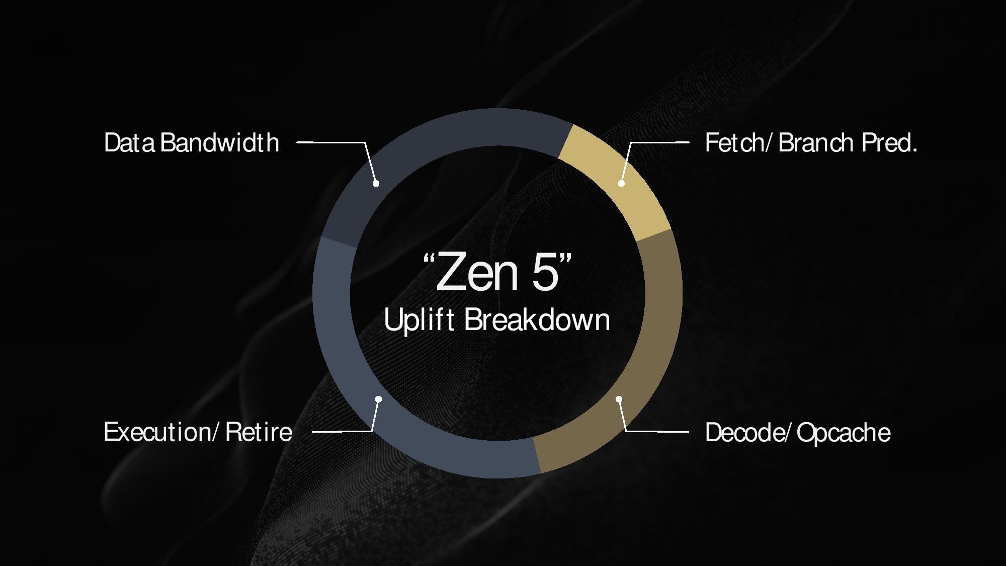
AMD quantified several of the various contributors to its 16% IPC improvement, with 34% of the gain being contributed by the move to an 8-wide execution/retire pipelines, 27% each from the decode/opcache and data bandwidth improvements, with the remaining 12% coming from the enhanced fetch/branch prediction.
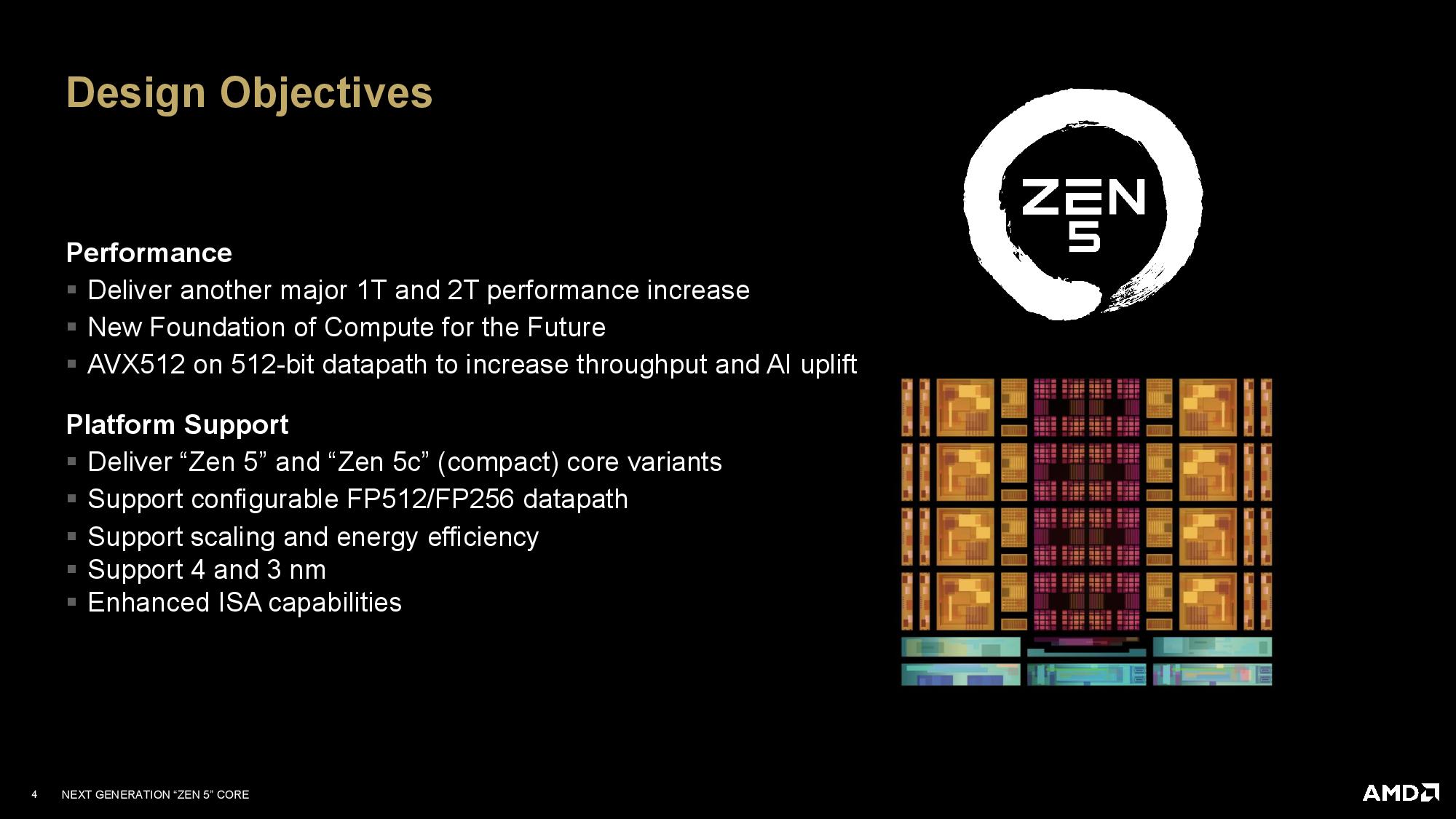
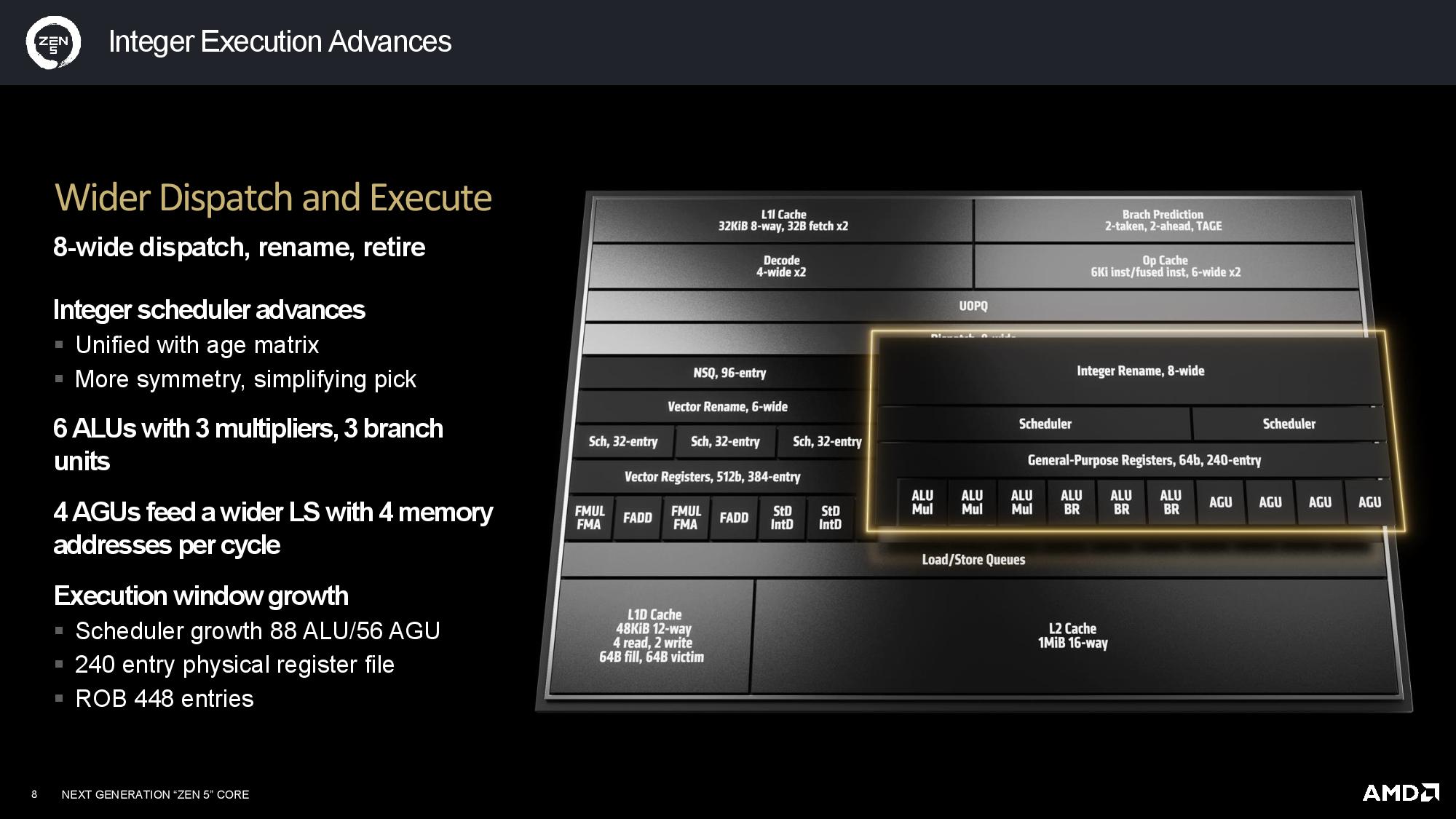
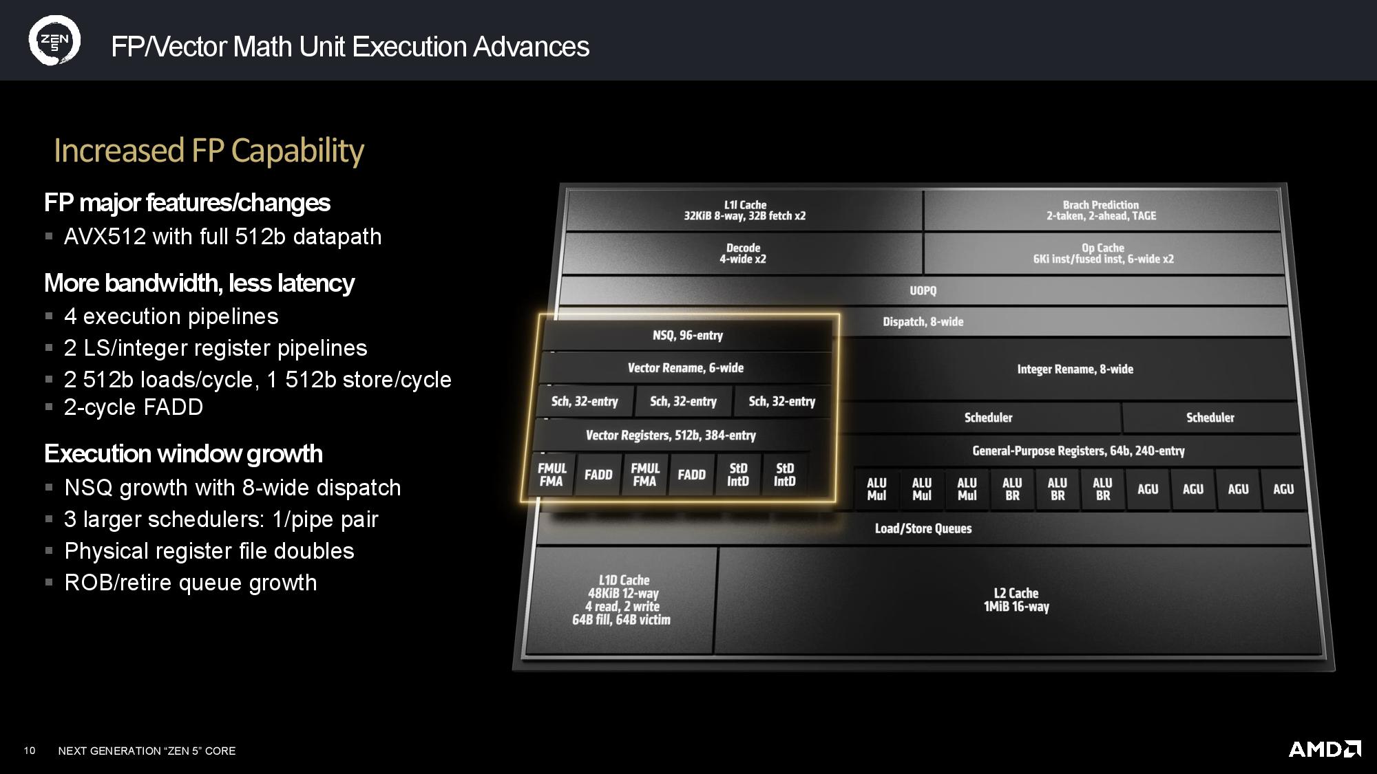
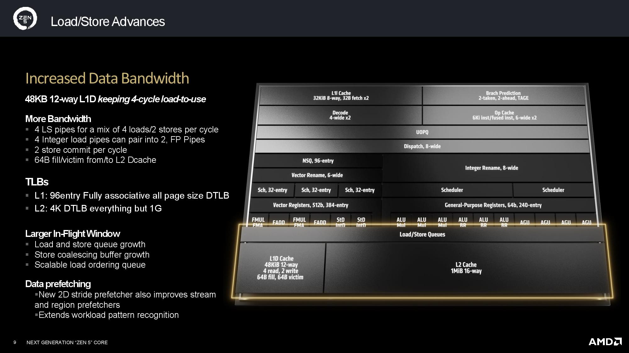
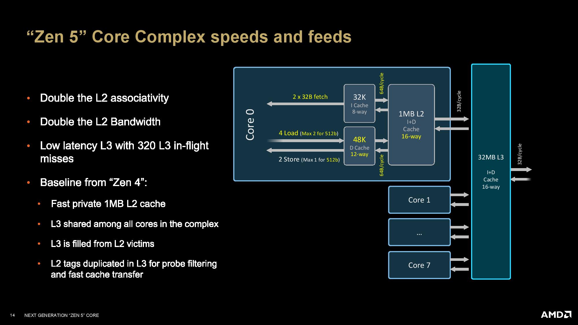
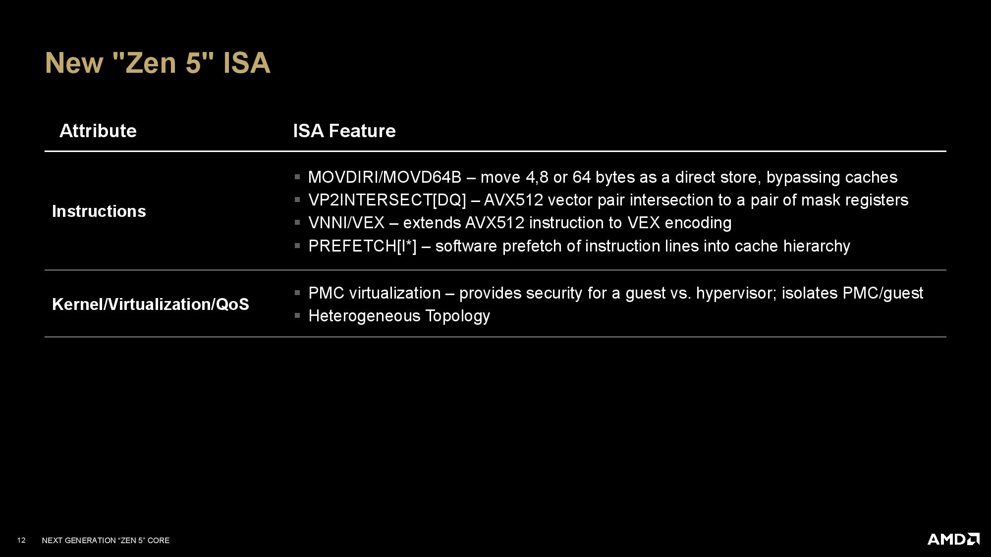
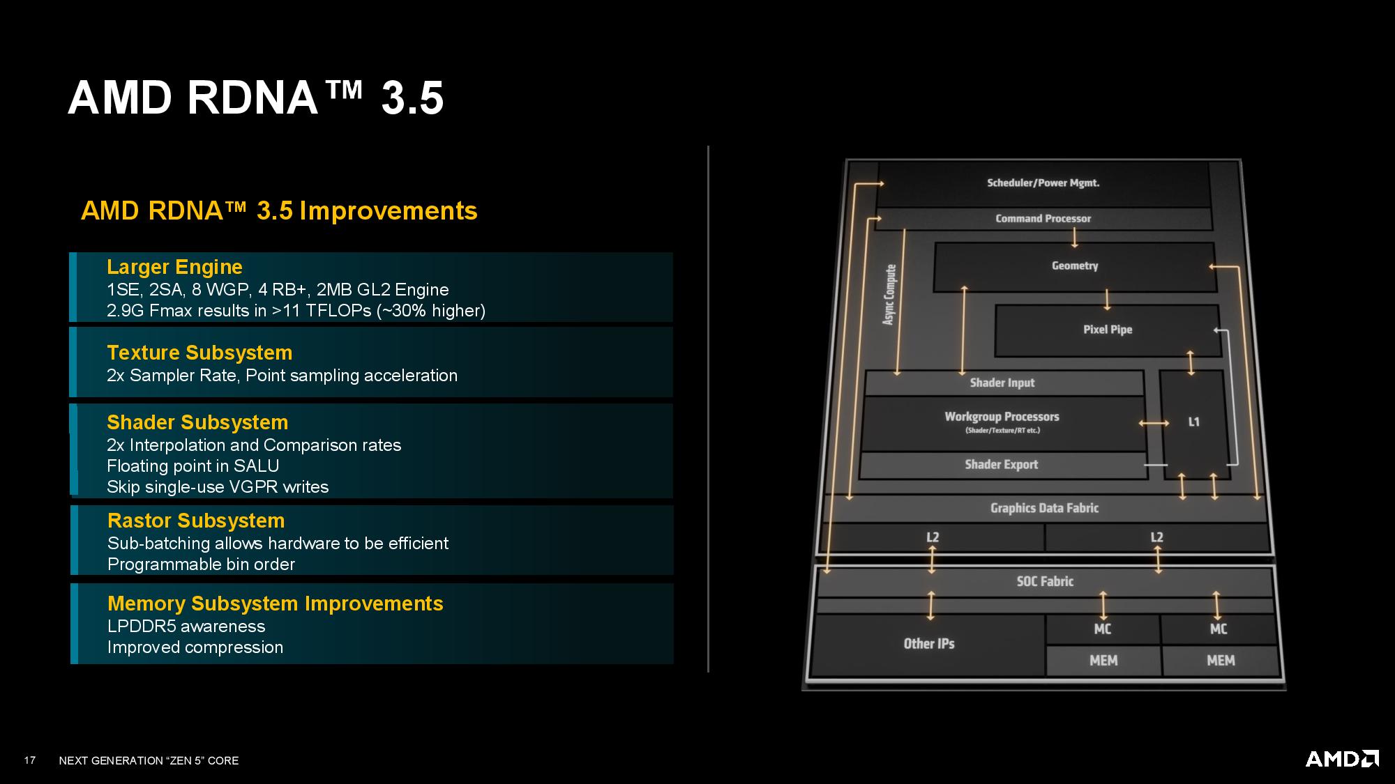
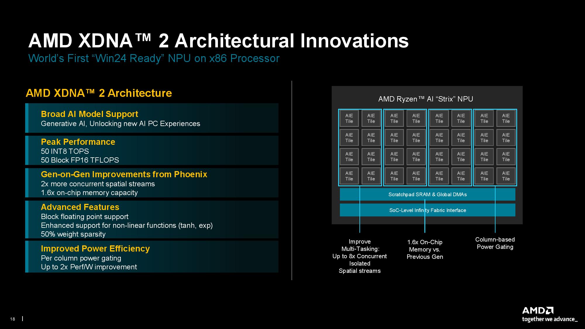
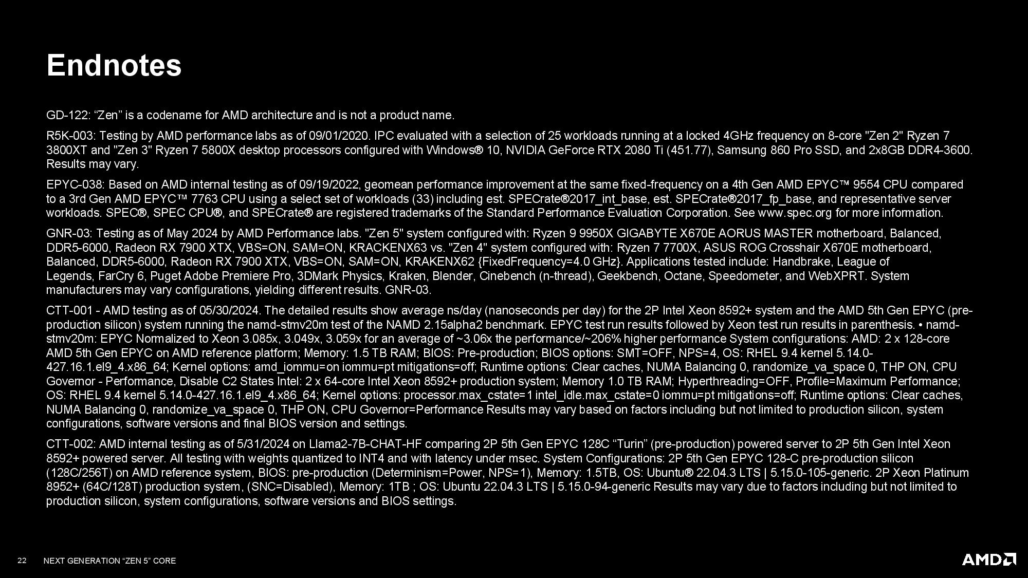
EDIT 7/24/2024: AMD shared more detailed slides in a later briefing, which we've included in the above album. We'll provide a more thorough write-up of the differences in our pending review.
Current page: Zen 5 Microarchitecture
Prev Page AMD Zen 5 Ryzen AI 300 ‘Strix Point’ Gaming and Productivity Benchmarks Next Page RDNA 3.5, XDNA 2 engine, and Thoughts
Paul Alcorn is the Editor-in-Chief for Tom's Hardware US. He also writes news and reviews on CPUs, storage, and enterprise hardware.
-
TerryLaze ReplyAdmin said:AMD revealed the deep-dive details of its Zen 5 Ryzen 9000 ‘Granite Ridge’ and Ryzen AI 300 series ‘Strix Point’ chips at its Zen 5 Tech Day.
AMD deep-dives Zen 5 — Ryzen 9000 and AI 300 benchmarks, Zen 5, RDNA 3.5 GPU, and XDNA 2 microarchitectures : Read moreTDP / PBP / MTP
Please don't use intel specific terminology on ryzen, they don't make any sense.
It's TDP and PPT only for ryzen. -
TerryLaze Also testing was done with a ~ $200 water cooler....just saying but if you need that to run the 9950x at stock, 230w ppt, then it's gonna be a joke, at least on the intel system you would get like ~350W out of that.Reply -
jeremyj_83 Reply
So if you can get more performance out of the AMD with a lower power draw that is a negative?TerryLaze said:Also testing was done with a ~ $200 water cooler....just saying but if you need that to run the 9950x at stock, 230w ppt, then it's gonna be a joke, at least on the intel system you would get like ~350W out of that. -
TerryLaze Reply
If you have to pay another $200 on top of the price of the CPU to get the performance that AMD claims then that is a bad thing.jeremyj_83 said:So if you can get more performance out of the AMD with a lower power draw that is a negative?
And I don't know how you do math but 230W of the 9950x is not lower than 230W of the 7950x
Being able to use 330-50W with the same cooling that another CPU can only use 230-50w with is a good thing because that means that if you use less power on it you will have much better temps.
Although we don't know, the other article shows the 9950x using 320W so maybe AMD chose to show overclocking numbers for their presentation, I honestly don't know which would be worse. -
jeremyj_83 Reply
Literally none of what you are saying makes sense. On top of that AMD might have used a $200 cooler to make sure that they couldn't be called out for hurting possible i9-14900k performance. Also note that at a 170W TDP the AMD chips have a 230W PPT and that is based on AM5 specifications.TerryLaze said:If you have to pay another $200 on top of the price of the CPU to get the performance that AMD claims then that is a bad thing.
And I don't know how you do math but 230W of the 9950x is not lower than 230W of the 7950x
Being able to use 330-50W with the same cooling that another CPU can only use 230-50w with is a good thing because that means that if you use less power on it you will have much better temps.
Although we don't know, the other article shows the 9950x using 320W so maybe AMD chose to show overclocking numbers for their presentation, I honestly don't know which would be worse. -
evdjj3j Reply
Wow, I lost some IQ points reading that.TerryLaze said:Also testing was done with a ~ $200 water cooler....just saying but if you need that to run the 9950x at stock, 230w ppt, then it's gonna be a joke, at least on the intel system you would get like ~350W out of that. -
TheSecondPower "The chips are also said to come with the new Lion Cove P-cores and Gracemont E-cores." That should say "Skymont E-cores." Gracemont is used in Alder Lake and Raptor Lake.Reply -
TerryLaze Replyjeremyj_83 said:Literally none of what you are saying makes sense. On top of that AMD might have used a $200 cooler to make sure that they couldn't be called out for hurting possible i9-14900k performance. Also note that at a 170W TDP the AMD chips have a 230W PPT and that is based on AM5 specifications.
It's not like it's a secret or in any way controversial that ryzen is very hard to cool.evdjj3j said:Wow, I lost some IQ points reading that.
The same amount of cooling that is required to get the PPT of ryzen at thermal throttle temps is enough to give intel 50% more power draw at 8 degrees lower temp.
https://www.anandtech.com/show/17641/lighter-touch-cpu-power-scaling-13900k-7950x/3

