AMD is allegedly readying budget hexa-core Krackan Point APUs — Hybrid 3+3 core "Zen 5 + Zen 5c" offering surfaces at Geekbench
Zen 5 APUs for the masses!

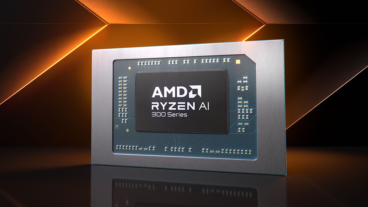
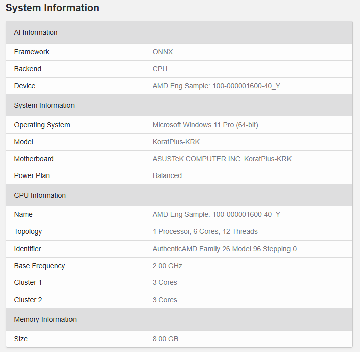
A new hexa-core processor under AMD's Krackan Point (KRK) lineup of APUs has emerged at Geekbench - thanks to Olrak at X. The CPU wields a rather unconventional 3+3 hybrid configuration - taking a different approach than AMD did with its Phoenix 2 APUs.
Krackan Point is AMD's cheaper alternative to Strix Point - packing upwards of eight cores and an eight Compute Unit (CU) RDNA 3.5-based iGPU (Integrated GPU). Krackan Point utilizes a hybrid-core design to save valuable die space, featuring up to four Zen 5 and four Zen 5c cores. The six-core offering has an OPN code of "100-000001600-40_Y," corresponding to a Ryzen 5 APU per previously leaked shipping manifests. The benchmark, being an AI test, isn't that exciting once you consider that Krackan employs the same 50 TOPS XDNA 2 NPU as Strix Point.
Going over the listed specs, the budget Ryzen 5 300 APU packs three Zen 5 and three Zen 5c cores alongside 12 threads - quite different from the Phoenix 2-based Ryzen 5 7545U - which had two Zen 4 and four Zen 4c cores. Moreover, the APU was being tested in an Asus validation platform and had a relatively low base frequency of 2 GHz - but that's likely a result of early silicon.

AMD reintroduced a dual-CCX design with Strix Point - splitting up the Zen 5 and Zen 5c cores across different rings - with separate L3 caches for both core types. Interestingly, for the Krackan Point APU in question, Geekbench divides the core count into two clusters. However, Olrak suggests that AMD might package all six cores together - connected through a unified ring bus - sharing a coherent L3 cache. To chip in, the Ryzen 5 7545U (Phoenix 2) also employed a single CCX, but the final decision rests on AMD.
Rest assured, laptops powered by AMD's Krackan Point offerings are set to arrive in early 2025 - starting at $799 if we go by leaks. Overall, CES 2025 will be jampacked with next-gen launches from all major players. Expect to see AMD unveil Krackan Point alongside Strix Halo APUs, Fire Range CPUs, and Radeon RX 8000 "RDNA 4" GPUs.
Get Tom's Hardware's best news and in-depth reviews, straight to your inbox.

Hassam Nasir is a die-hard hardware enthusiast with years of experience as a tech editor and writer, focusing on detailed CPU comparisons and general hardware news. When he’s not working, you’ll find him bending tubes for his ever-evolving custom water-loop gaming rig or benchmarking the latest CPUs and GPUs just for fun.
-
usertests ReplyRest assured, laptops powered by AMD's Krackan Point offerings are set to arrive in early 2025 - starting at $799 if we go by leaks.
Lol pricing. It reminds me of AMD pitching Mendocino as a $700 laptop chip. Krackan/Kraken is clearly better than Memedocino, but not necessarily better than discounted Hawk Point systems on the market because of the graphics (8 CUs max).
VideoCardz hallucinated 4 CUs for the 6-core. There's nothing to corroborate that, but it could be correct. If true, it would at least match Phoenix2's CU count, but it would only be interesting if it was very cheap, say sub-$300.
I don't think consumers care at all for the NPU and Copilot+. AMD needs to invent some use cases if Microsoft is going to drop the ball for everybody. Get your own streaming video upscaler to use the NPU and convert 480p to 1080p/4K, and maybe leverage XDNA2 for FSR4. But the point is that this capability obviously not justify pushing systems with a tiny, cheap die to $700-800. -
Cooe Kraken will most DEFINITELY have all 8x cores (4x Zen 5+ 4x Zen 5c) on the same, single unified ring bus. There is quite literally ZERO technological reason for them not to. 🤷Reply
Geekbench presenting them as two different clusters is just how it deals with multiple core types on any CPU, REGARDLESS of how they are laid out/connected internally on the chip itself! If the cores on a CPU are different from each other in ANY major spec (ISA support, cache sizes, etc...) then Geekbench will list them out as separate "clusters".
And the reason why AMD's Strix Point has two separate rings connected w/ crossbars (think old-school big die Xeon style, or AMD Zen 4/5c "dense" 16-core CCD style for a more modern example lol) instead of a single unified ring for all 12x cores didn't have ANYTHING to do with it having "two different "CPU core types" on the same CPU", and EVERYTHING to do with the fact that AMD's current ring bus tech (which originated on Zen 3 w/ its then new unified CCX's) cannot handle more than 8x cores on a ring... Aka the exact same number of cores on a standard Zen CCD.
AMD has made it repeatedly clear with their CPU die designs over the past couple years that anything >8-cores on a single die needs >1x ring bus + the extra crossbar links to connect them with their current bus technology. 🤷
(Again, see literally every Zen c/"dense" CCD design made so far AND Strix Point all having literally the EXACT SAME CPU bus layout! ) -
subspruce Reply
4+4 is going to be another SKU and 3+3 is going to be bottom of the barrelCooe said:Kraken will most DEFINITELY have all 8x cores (4x Zen 5+ 4x Zen 5c) on the same, single unified ring bus. There is quite literally ZERO technological reason for them not to. 🤷
Geekbench presenting them as two different clusters is just how it deals with multiple core types on any CPU, REGARDLESS of how they are laid out/connected internally on the chip itself! If the cores on a CPU are different from each other in ANY major spec (ISA support, cache sizes, etc...) then Geekbench will list them out as separate "clusters".
And the reason why AMD's Strix Point has two separate rings connected w/ crossbars (think old-school big die Xeon style, or AMD Zen 4/5c "dense" 16-core CCD style for a more modern example lol) instead of a single unified ring for all 12x cores didn't have ANYTHING to do with it having "two different "CPU core types" on the same CPU", and EVERYTHING to do with the fact that AMD's current ring bus tech (which originated on Zen 3 w/ its then new unified CCX's) cannot handle more than 8x cores on a ring... Aka the exact same number of cores on a standard Zen CCD.
AMD has made it repeatedly clear with their CPU die designs over the past couple years that anything >8-cores on a single die needs >1x ring bus + the extra crossbar links to connect them with their current bus technology. 🤷
(Again, see literally every Zen c/"dense" CCD design made so far AND Strix Point all having literally the EXACT SAME CPU bus layout! )