AMD unwraps Ryzen AI 300 series ‘Strix Point’ processors — 50 TOPS of AI performance, Zen 5c density cores come to Ryzen 9 for the first time
AI hits overdrive
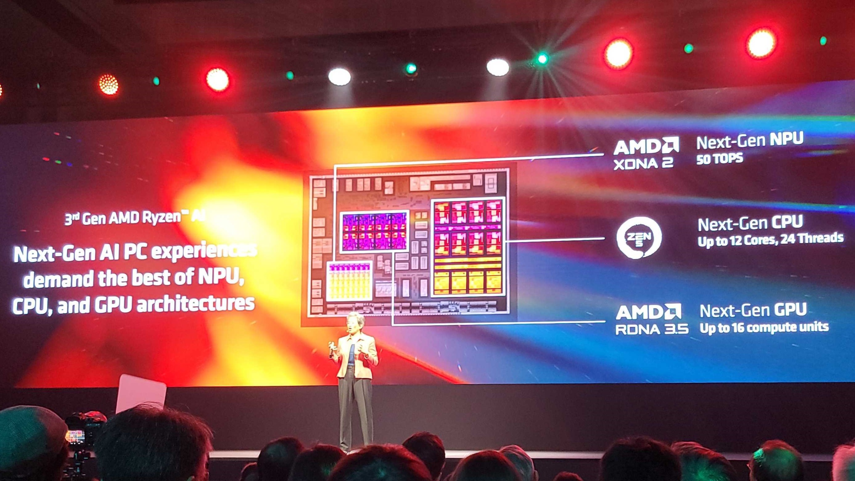
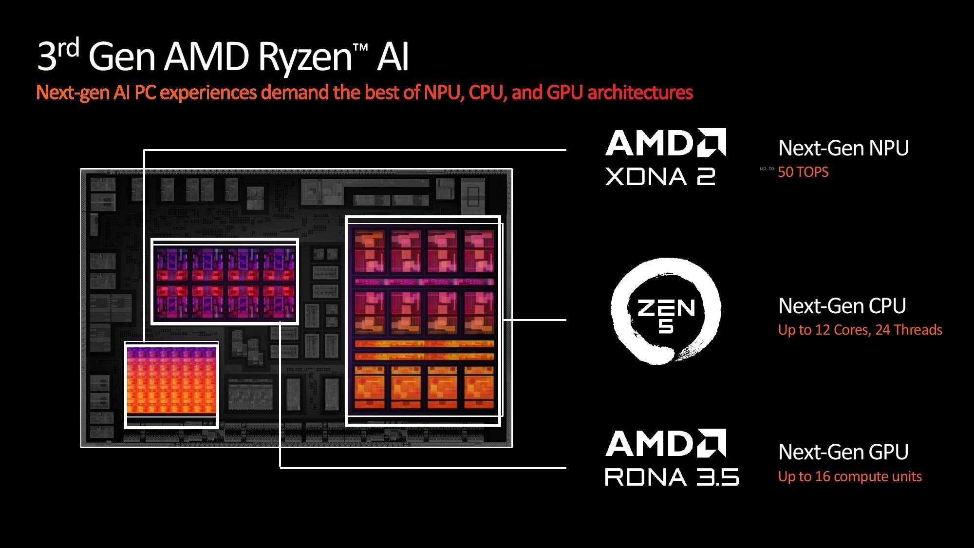
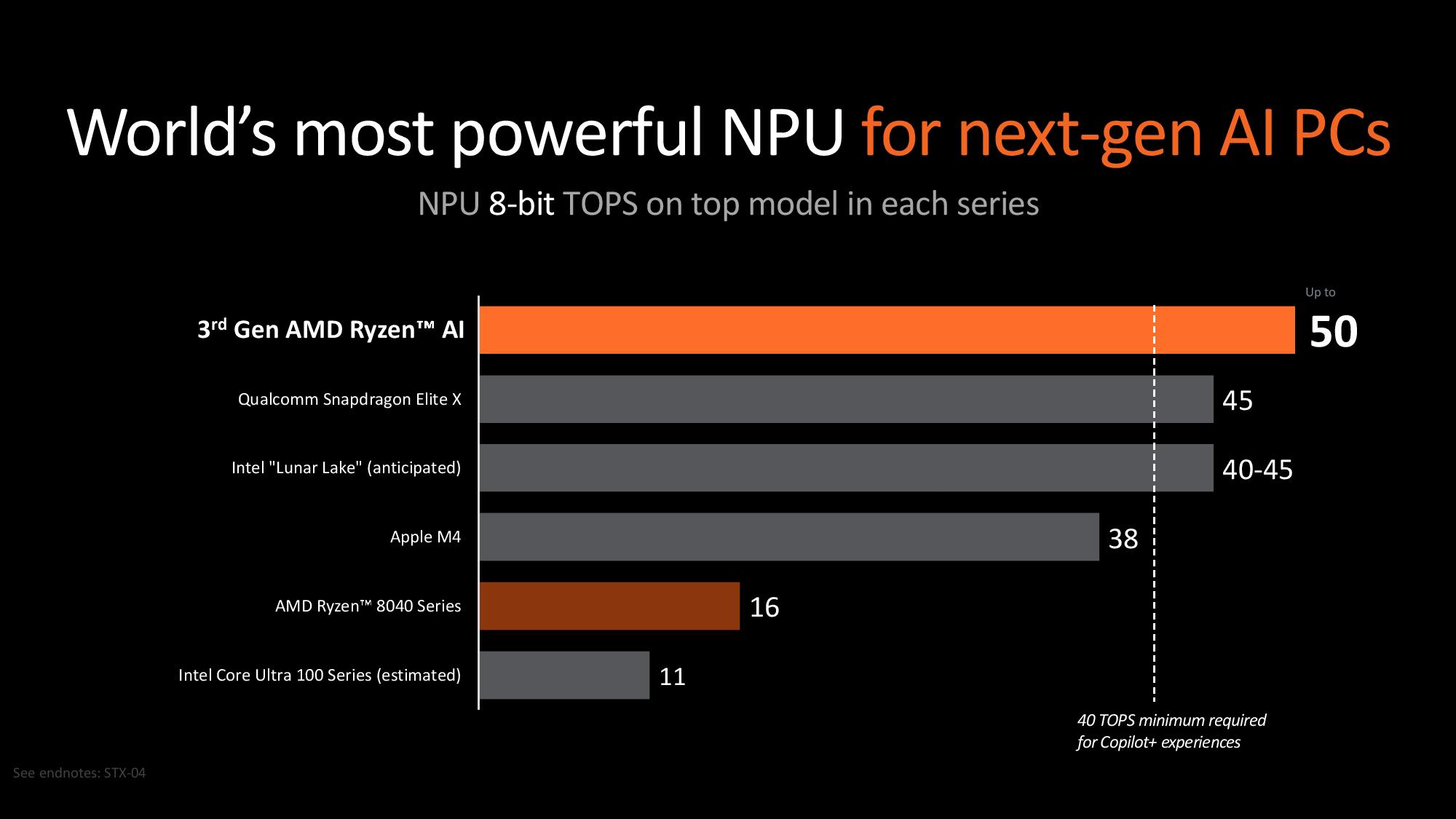
AMD unwrapped its new Ryzen AI 300 series, codenamed Strix Point, today at Computex 2024 here in Taipei, Taiwan, with the new chips featuring the new Zen 5 CPU microarchitecture with two types of cores, an upgraded RDNA 3.5 graphics engine, and of course, AMD’s new XDNA 2 engine that enables running AI workloads locally. AMD’s new branding scheme now brings ‘AI’ right into the name of the chip, reflecting the company’s strong focus on its new AI-focused XDNA 2 neural processing unit (NPU) that now offers 50 TOPS of performance, a 5X gain for the third generation of AMD’s AI processors. This level of performance beats all other chips for Windows PCs, including Qualcomm’s promising Snapdragon X Elite. It easily exceeds Microsoft’s 40 TOPS requirement for next-gen AI PCs, allowing Copilot elements to run locally.
AMD has plenty of other advances under the hood, too, with a move to 12-core Zen 5 processors for thin-and-light and ultralight notebooks that used to be limited to eight CPU cores and up to 16 compute units for the new RDNA 3.5 integrated graphics engine, an increase over the previous-gen’s maximum of 12 CUs.
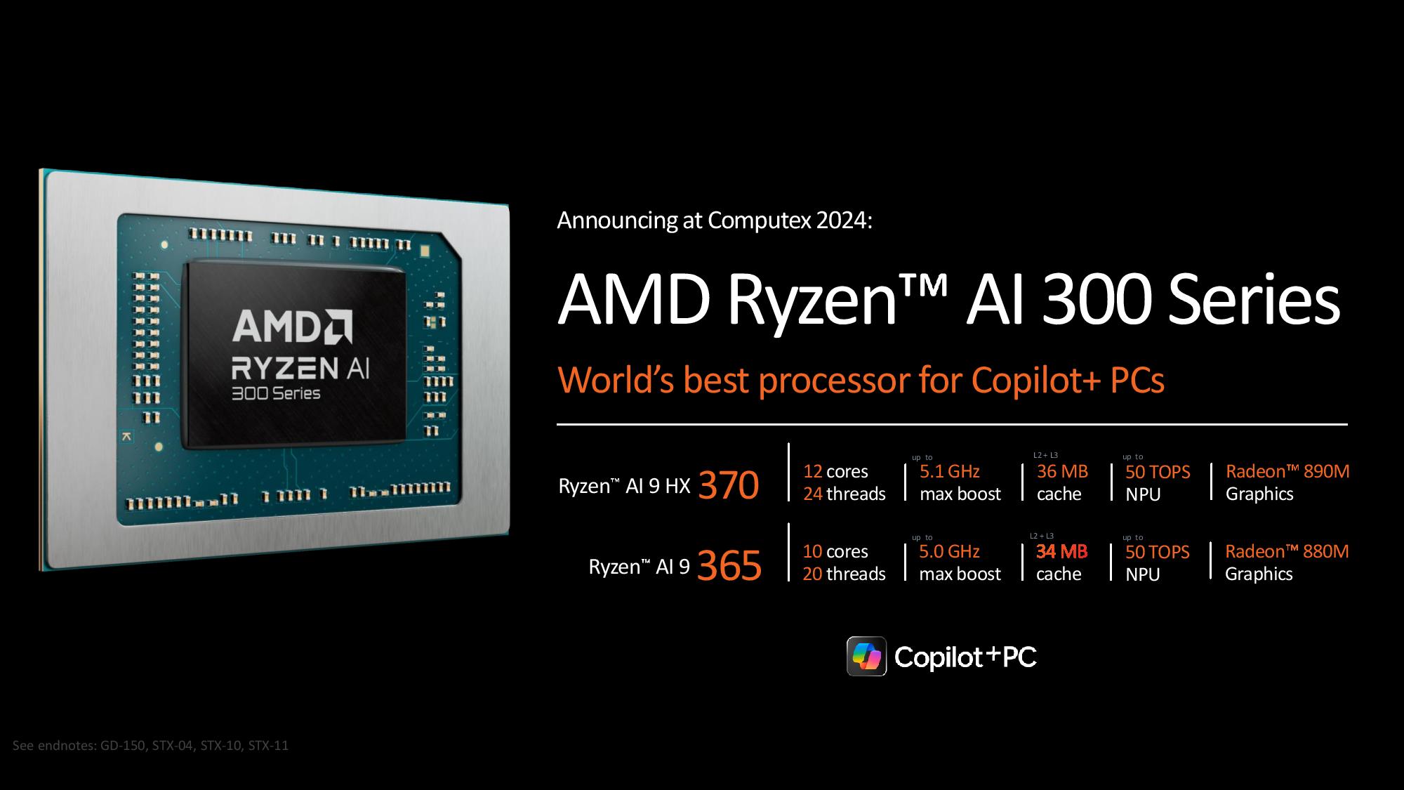
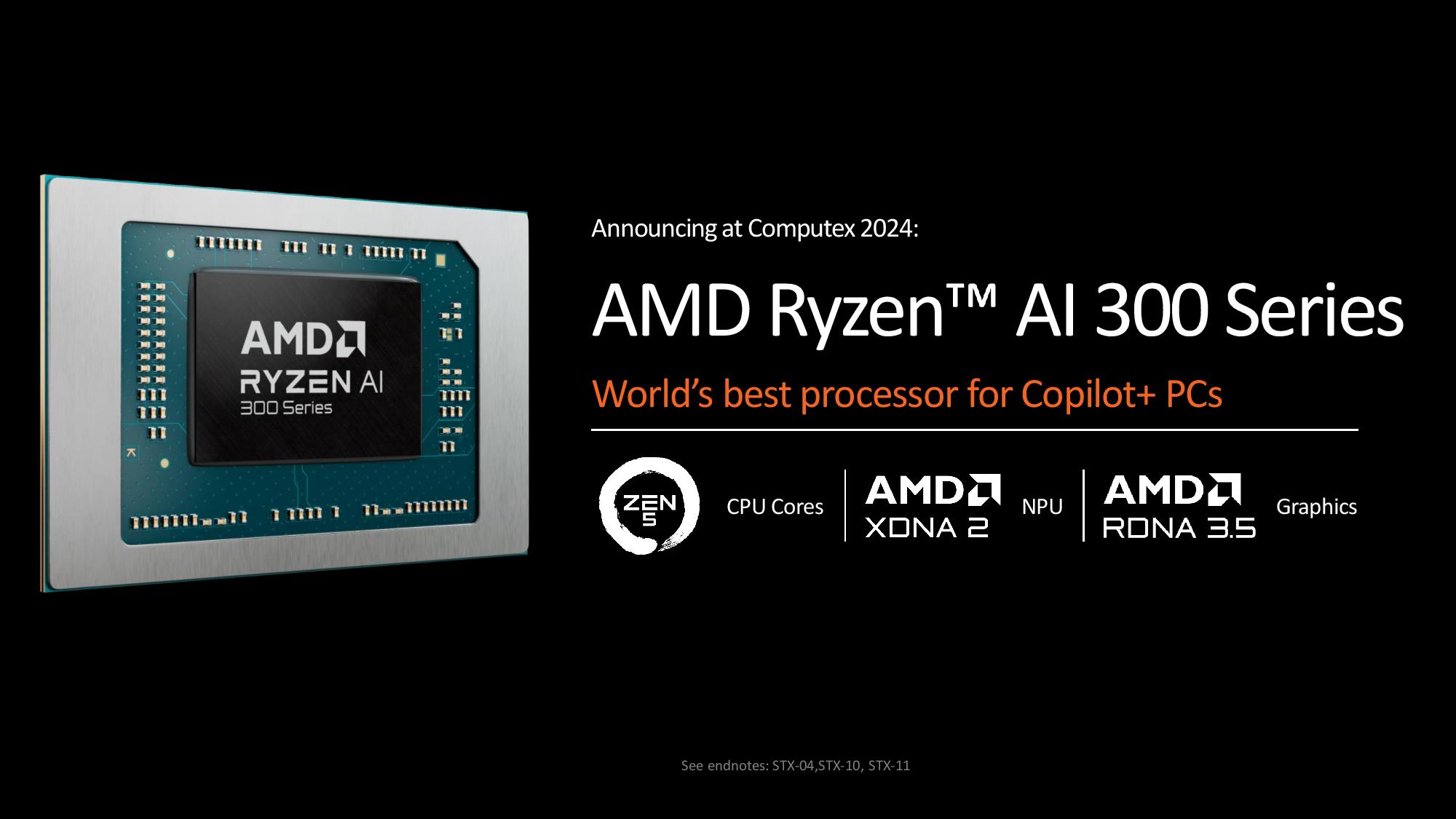
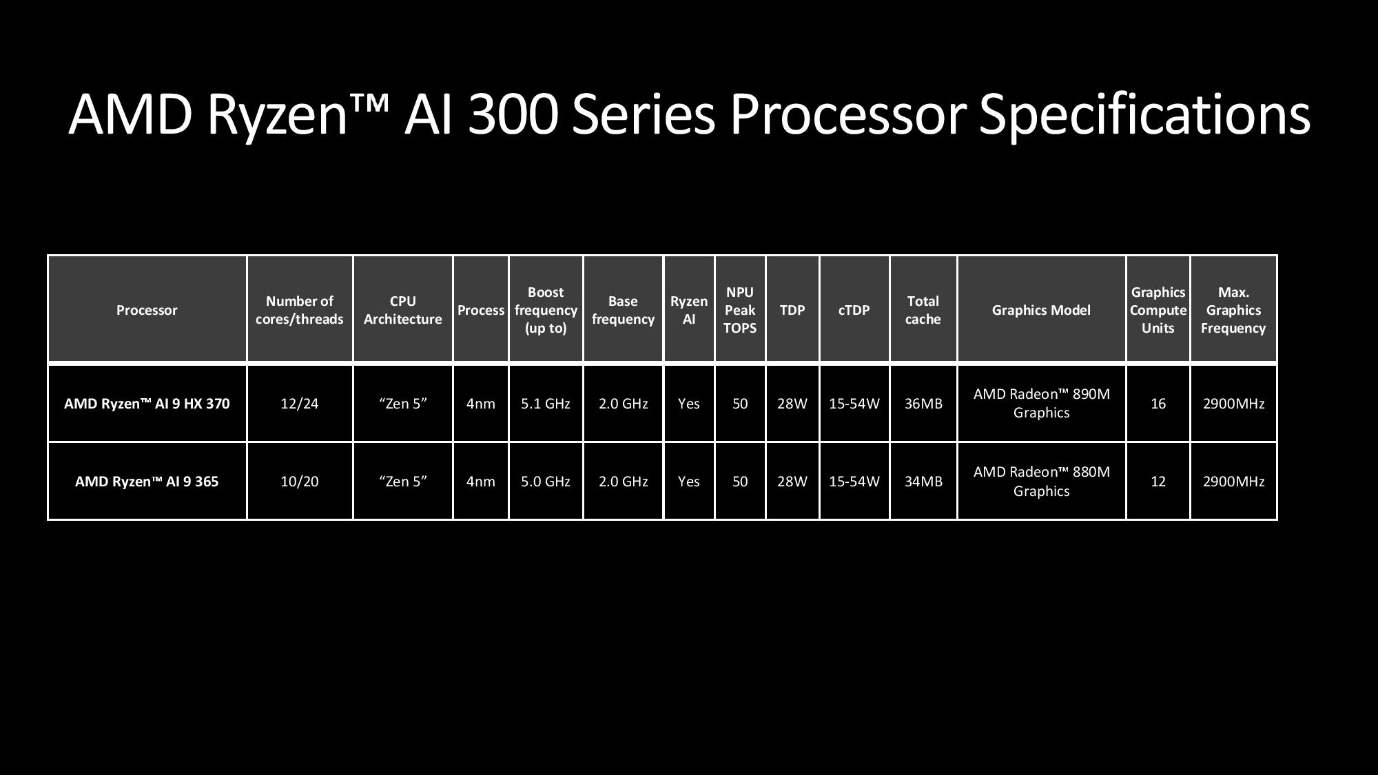
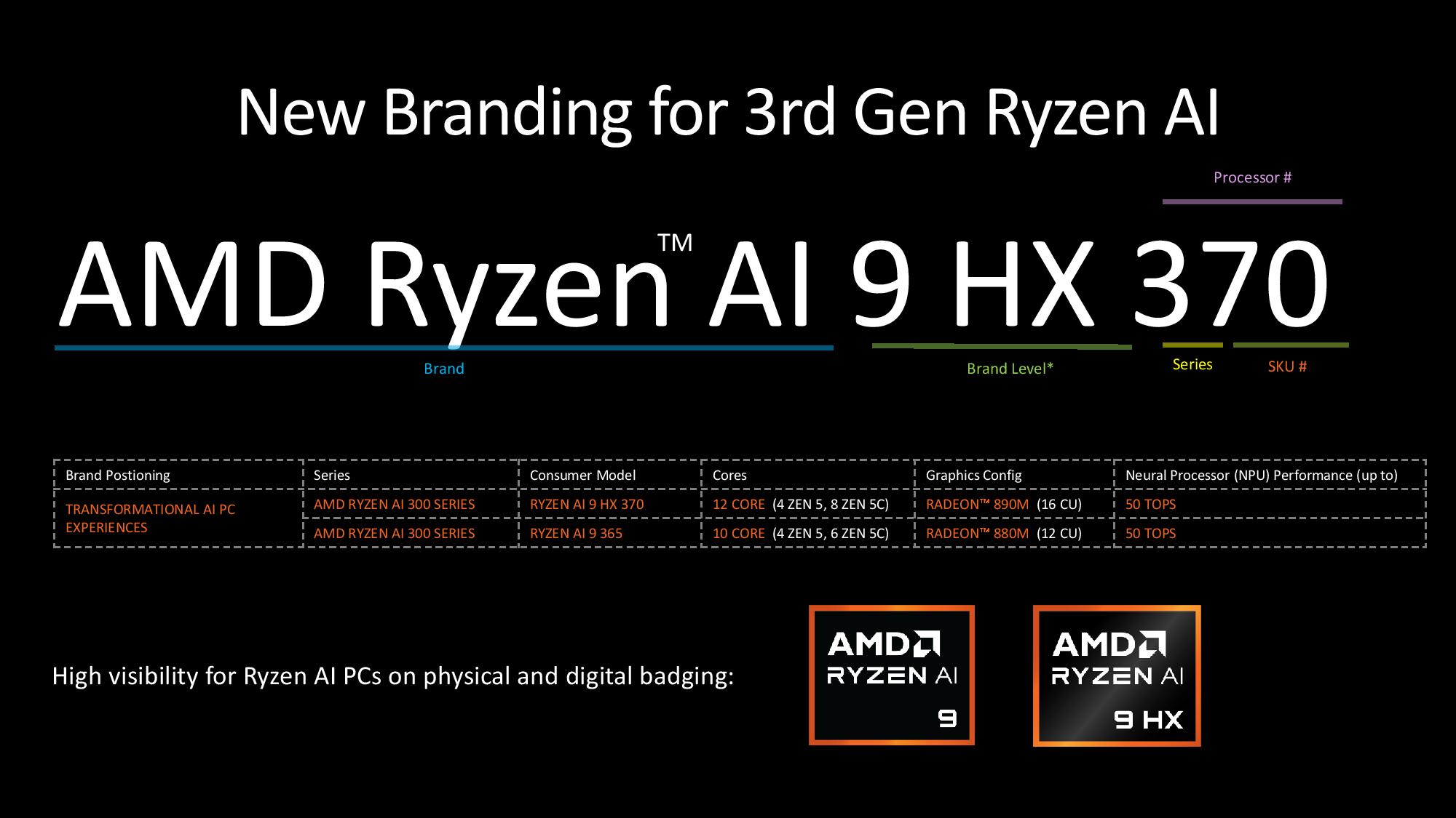
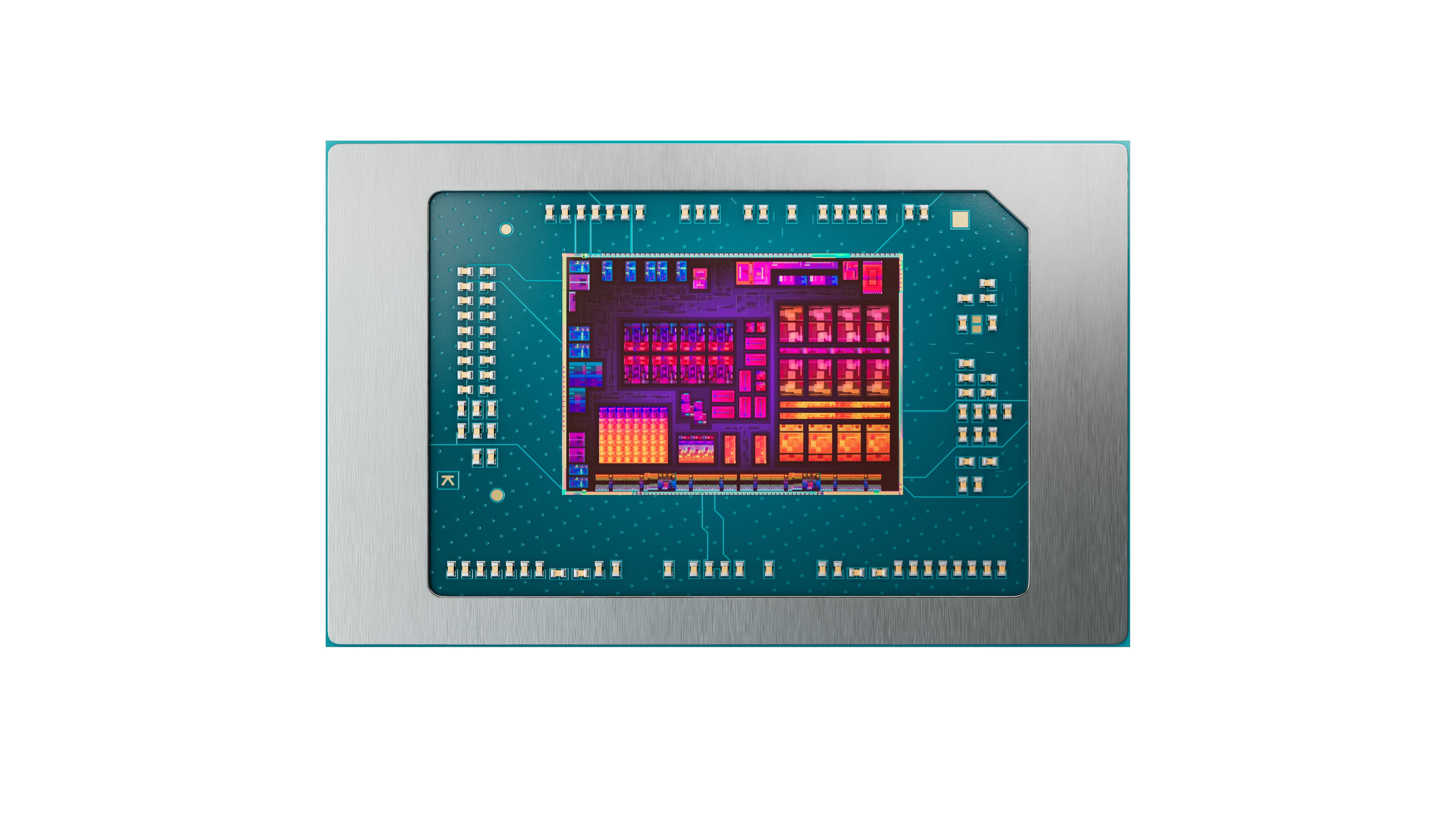
The Ryzen AI 300 series launches with two new models, and as you can see in the slides above, these chips come as a single monolithic die. The flagship Ryzen AI 9 HX 370 has 12 cores and 24 threads that operate at a base of 2.0 GHz and a peak of 5.1 GHz. However, as you can see in the block diagram and listed in a branding slide, the chip has four standard Zen 5 cores and eight density-optimized Zen 5c cores on a single monolithic die with the GPU and NPU cores.
This marks the debut of the smaller Zen 4C cores in the highest-tier Ryzen 9 mobile family, as these cores were previously limited to AMD’s lowest-end Ryzen 5 and 3 models with the prior-gen Hawk Point chips. AMD's Zen 5c cores are designed to consume less space on a processor die than the 'standard' Zen 5 performance cores while delivering enough performance for less demanding tasks, thus saving power and delivering more compute horsepower per square millimeter than was previously possible (deeper dive here). Though this technique is conceptually similar to Intel's E-cores, AMD’s Zen 5c employs the same microarchitecture as the standard Zen 5 cores and supports the same features with its smaller cores. In contrast, Intel’s design employs different architectures and feature support. Still, the smaller Zen 5c cores operate at lower clock rates and thus offer less peak performance than standard cores, but they also preserve die area for other additives, like a larger GPU and NPU.
The standard and density-optimized Zen 5c cores both support threading, but we assume the higher boost clock only applies to the four standard cores (AMD hasn’t shared detailed specs of the Zen 5c cores yet). The HX 370 chips also have 36 MB of total L3 cache, the 50 TOPS XDNA 2 NPU, and the new RDNA 3.5 Radeon 890M graphics engine with 16 CUs that run at 2.9 GHz. The chip has a 28W TDP rating, but its broad cTDP range means that will not reflect its actual operating power level, which we’ll cover below.
The Ryzen AI 9 365 has ten cores, spread among four standard Zen 5 cores and six density-optimized Zen 5C cores, with a base of 2.0 GHz and a peak boost of 5.0 GHz. The chip also has the 50 TOPS NPU and a 12-CU RDNA 3.5 Radeon 880M graphics engine running at 2.9 GHz. Despite the lower CPU and GPU core counts, this chip is also listed with a 28W TDP like its bigger brother, though this rating is now of dubious importance.
AMD’s previous-gen 7040 and 8040 families were comprised of nine models, so the two new Ryzen AI 300 models are obviously just AMD’s first salvo in its new AI-focused lineup. Below, we’ll cover the specs, what we know about the architecture and process node, AMD’s new branding scheme, and AMD’s benchmarks.
Get Tom's Hardware's best news and in-depth reviews, straight to your inbox.
Zen 5, Zen 5c, and RDNA 3.5
AMD divulged that its new Zen 5 microarchitecture delivers a 16% increase in IPC over Zen 4. Paired with new process technology (purportedly TSMC 4nm), the new chips should deliver big gains in both performance and power efficiency at any given power level—particularly with the addition of Zen 5c cores. You can read more about the Zen 5 architecture here.
AMD pairs the new CPU cores with its RDNA 3.5 integrated graphics with up to 16 CUs, a notable increase over the previous peak of 12 CUs. AMD hasn’t shared any fine-grained information on the changes with the new graphics architecture, but we expect more information to surface as the chips move closer to market.
Untangling the New Ryzen AI 300 Series Branding
AMD’s new AI branding is an eye-catcher. Aside from using ‘AI’ right in the brand name, AMD also realigned its entire naming scheme, a curious decision given that it had previously announced a rather complex new branding scheme for its mobile lineup that required a decoder ring to navigate. AMD originally said that it expected the new naming scheme to last five years, but given the shift to next-gen AI PCs, the company has now pivoted to AI-specific branding a mere one and a half years later.
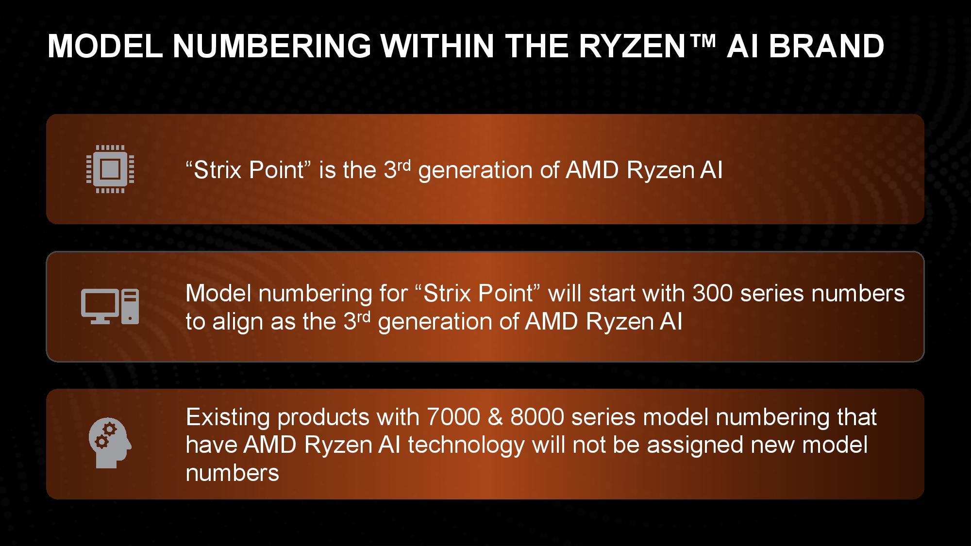
In many respects, the new branding is easier to comprehend, at least insofar as it doesn’t require a decoder ring like the previous scheme but is also a bit more ambiguous. AMD’s model numbering reset begins with the 300 series, so named because Strix Point is the third series of AMD’s mobile AI chips with an NPU. The 7040 ‘Phoenix’ and 8040 ‘Hawk Point’ chips were the first two generations, respectively, but the older models will retain their current branding -- the new branding scheme only applies to Strix Point and newer generations.
AMD’s previous-gen chips were carved into swim lanes defined by the TDP, like U-, HS- and H-series (15/28W, 35W, 45W TDPs, respectively), but Strix Point marks a fundamental shift and no longer has a designator for the TDP level. Any Strix Point chip can be assigned from a 15W to a 54W cTDP (configurable TDP) threshold by the OEM, just as with the previous-gen models, but this will now become a more common practice. As such, AMD doesn’t feel the need to call out the TDP rating as a designator in the product name.
I asked AMD how its customers would know which laptops run at a 15W or a 54W TDP despite having the same CPU model name. AMD says this approach is similar to what they are already doing with cTDPs, and the intention is to simplify the buying decision for mainstream buyers at box stores like Best Buy. Unfortunately, this is not entirely unlike Intel’s own policy of not requiring OEMs to divulge cTDP specifications. As such, you’ll need to check reviews to ensure you’re getting a capable machine.
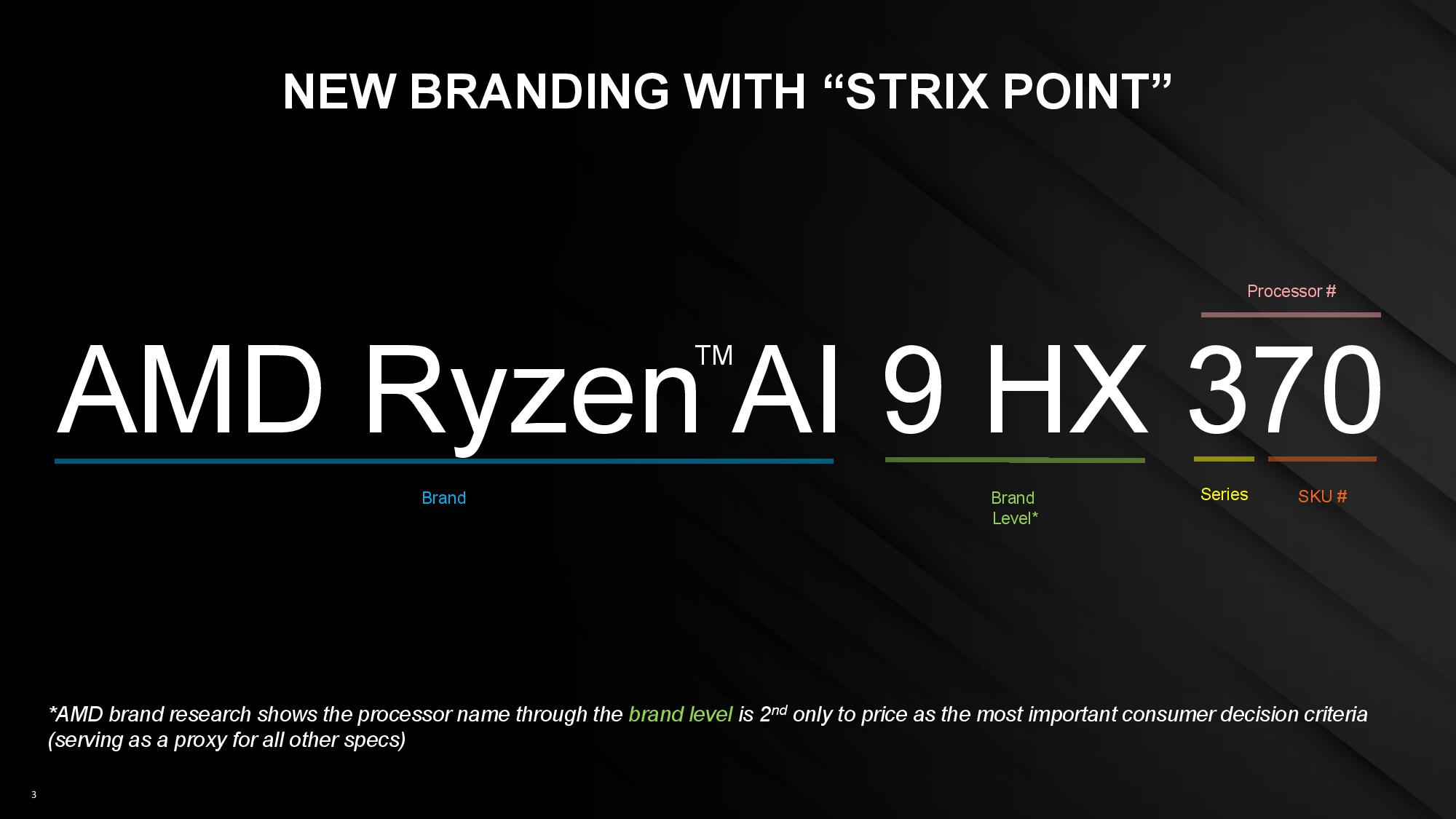
With TDP removed as a branding measuring stick, the new designators merely signify a ‘brand level.’ For instance, the Ryzen AI 9 HX 370 moniker specifies that the chip is a Ryzen 9 model in the HX category, with the HX designator denoting it’s a high-performance top-of-stack model. The last three digits denote the processor number, with the first digit indicating the series (in this case, 300 series) and the last two digits signifying the relative positioning of the chip within that series (for instance, a ‘350’ chip would be lower than the ‘370’). AMD also unveiled new badges with the new Ryzen branding.
AMD XDNA 2 NPU Architecture
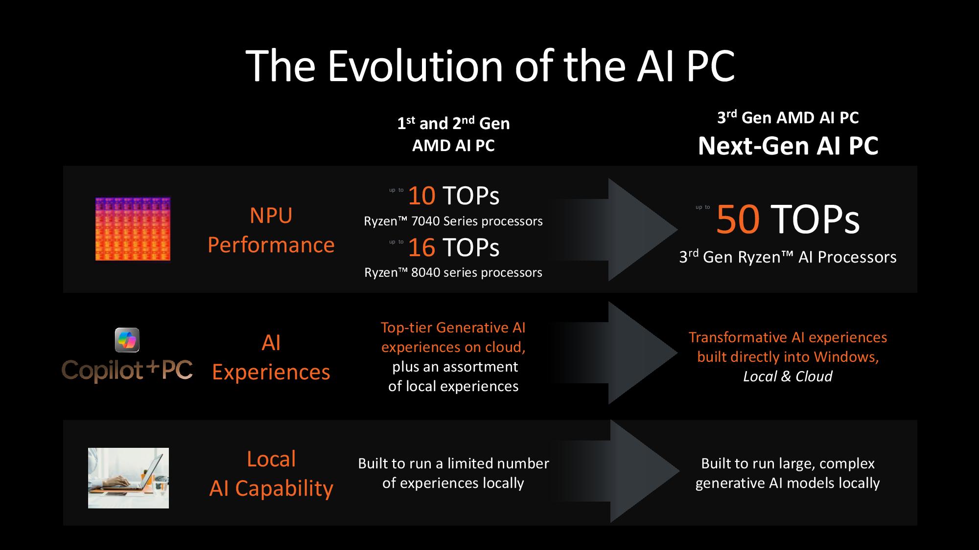
AMD shared plenty of details about its new AI-accelerating XDNA 2 neural processing unit (NPU). AMD was the first x86 chipmaker to bring an NPU to both the mobile and desktop PC markets, with its first-gen Phoenix chips delivering 10 TOPS of performance. That then progressed to 16 TOPS with the Hawk Point refresh, mostly due to boosted NPU clock speeds.
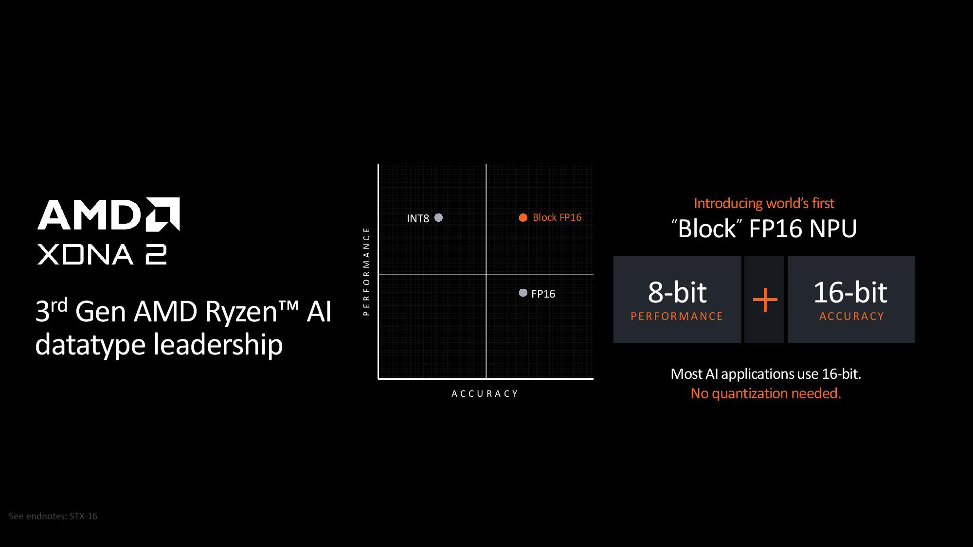
AMD’s Strix Point takes AI performance to a whole new level. The re-architected XDNA 2 engine delivers up to 50 TOPS of performance in both INT8, which is how most NPU metrics are spec’d, and Block FP16, a new paradigm we’ll dive into shortly. AMD hasn’t yet shared the full TOPS rating for its chips with the CPU and GPU added in.
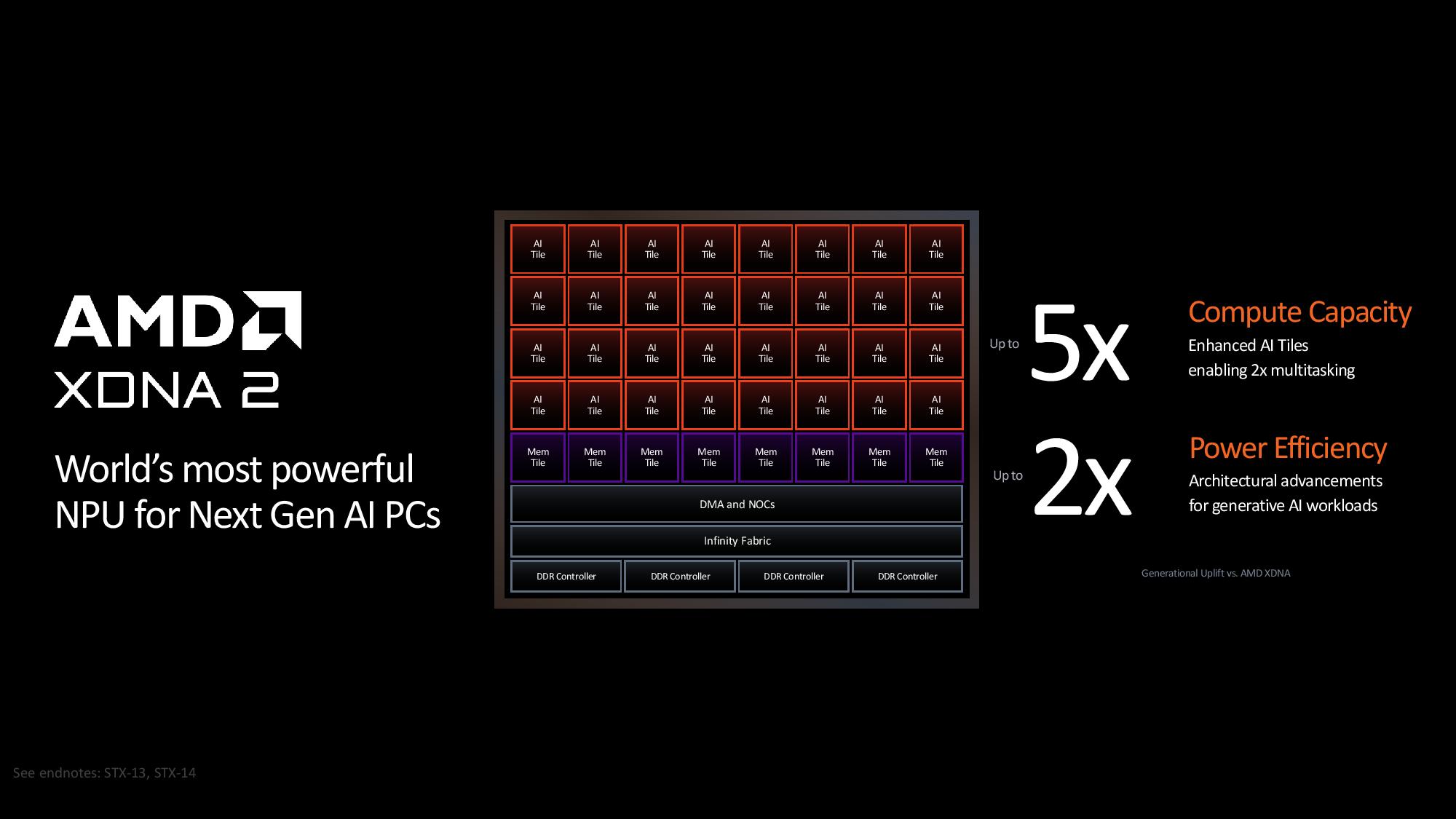
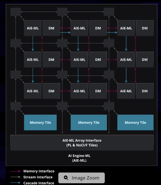
Here, we can see the block diagram of the new XDNA 2 engine, and we have the XDNA 1 engine in the following slide. As you can see, there are 3.5x more ‘AI tiles,’ which previously were referred to as AIE-ML units. It appears that the DM units (used for scalar calculations) have been merged into the new AI tile. The new engine is seemingly far more complex and thus performant, but we’ll have to wait for a proper architectural briefing for more details.
AMD’s rearchitecting of its XDNA 2 engine, which was borne of its Xilinx IP when AMD purchased the company, yields a fivefold increase over the first-gen XDNA to 50 TOPs and twice the power efficiency. The enhanced power efficiency is a critical advance, as the primary goal of the NPU is to offload AI tasks to save battery life.
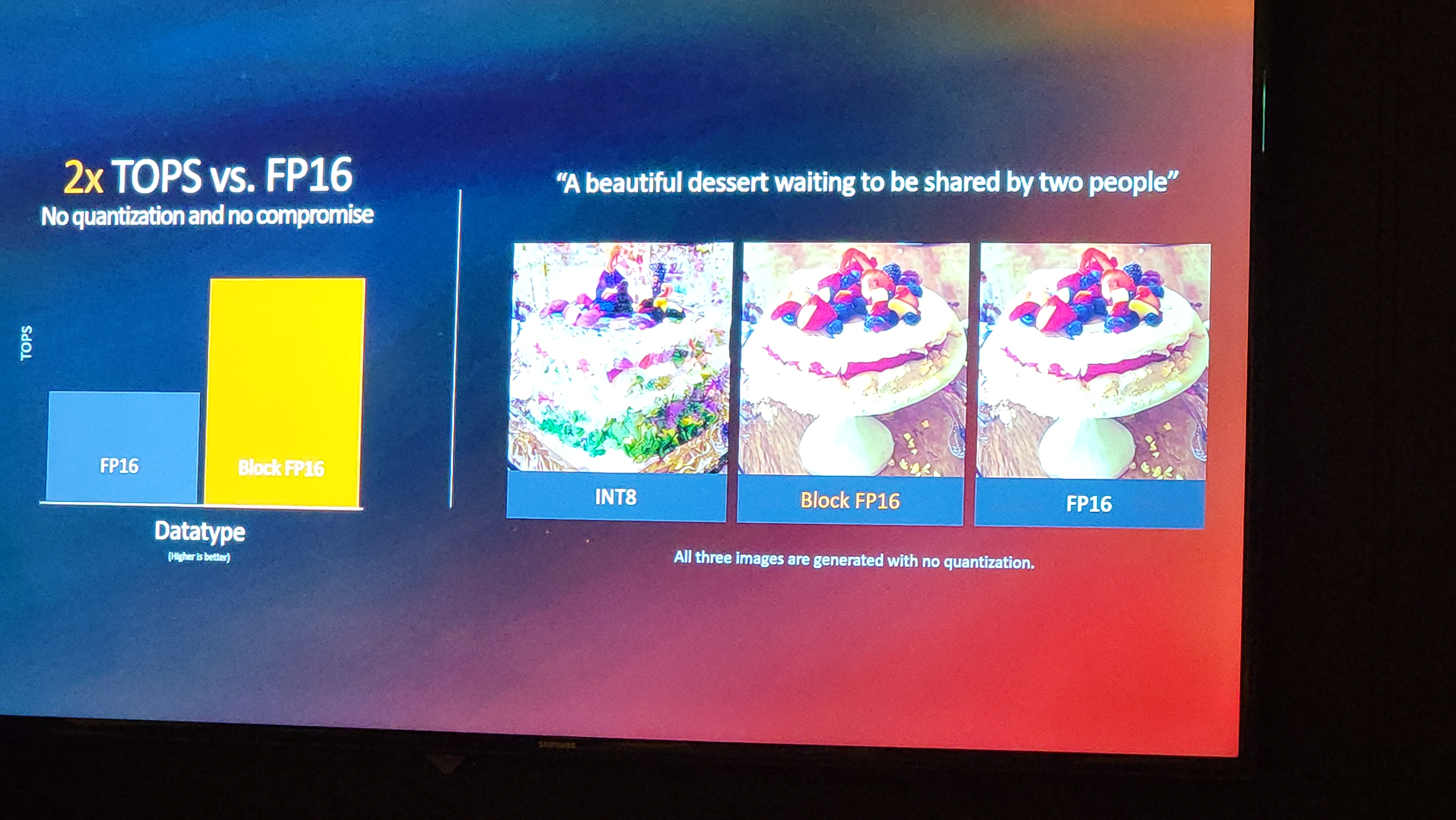
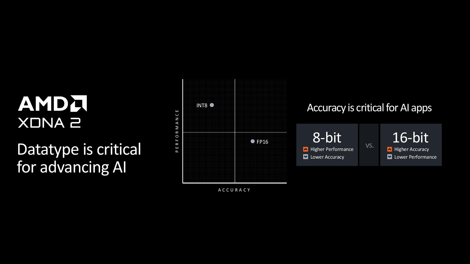
NPUs are typically characterized by performance in INT8 workloads, a less-precise data type that uses less compute and memory to run a model. However, models have to be quantized to the INT8 format and lose a bit of precision in the process. AMD’s XDNA 2 is the first x86 NPU to support Block BF16, a new data format that provides the full accuracy of FP16 with many of the same compute and memory characteristics of INT8. AMD says Block FP16 is plug-and-ply; it doesn’t require quantizing, tuning, or retraining the existing models.
As such, AMD has the only NPU on the market that supports not only 50 TOPS with INT8 but also a full 50 TOPS with Block FP16. The company showcased a benchmark using both INT8 and Block FP16 to run the same Stable Diffusion prompt to generate an image, the latter of which provided a more accurate image more quickly. It isn’t yet clear if Block FP16 is certified as an IEEE standard.
AMD Ryzen 9 AI 300 Series Benchmarks
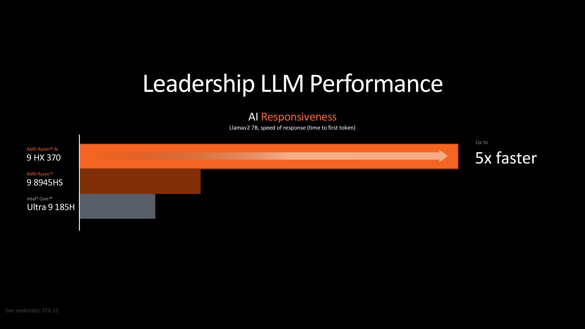
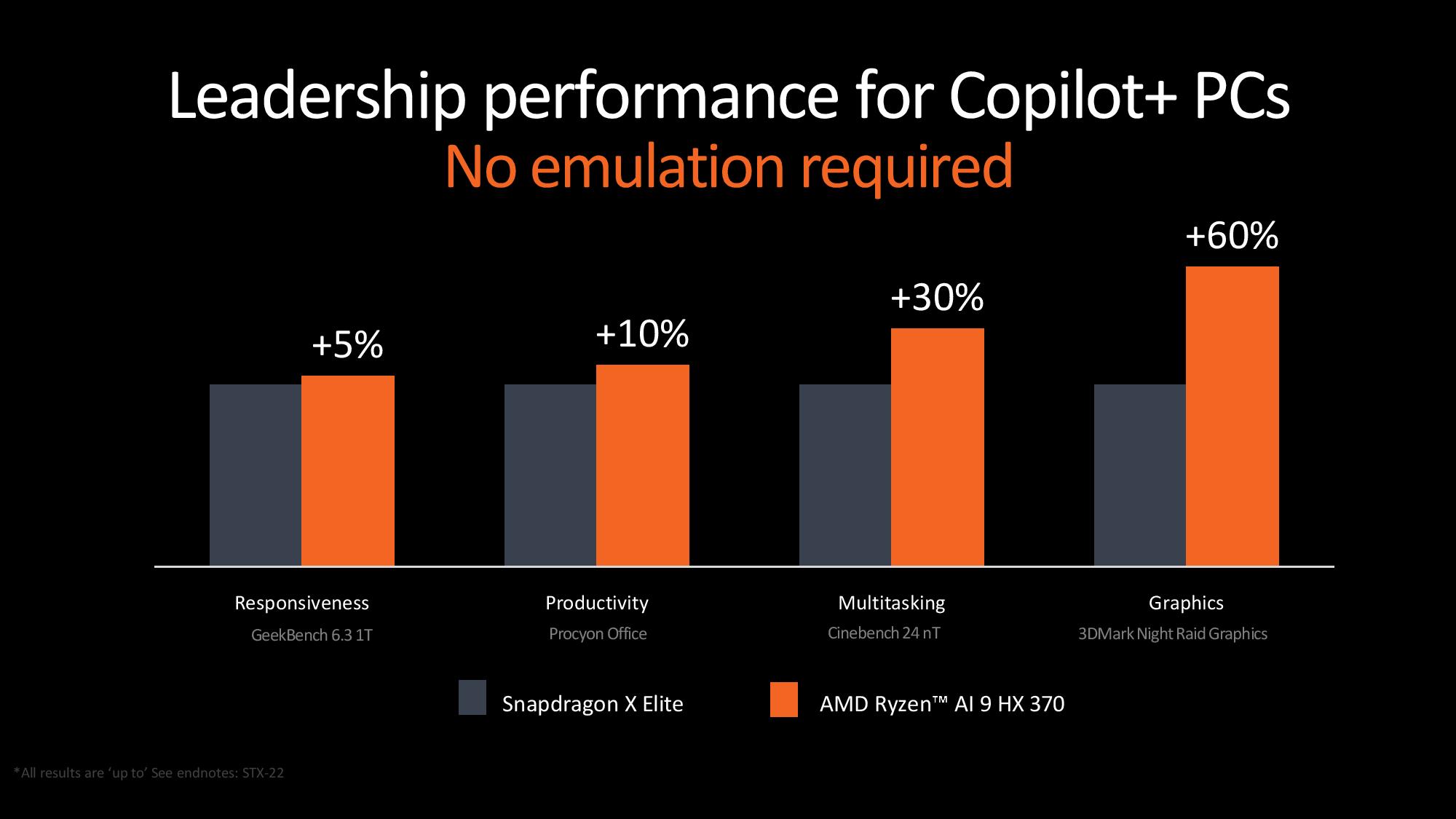
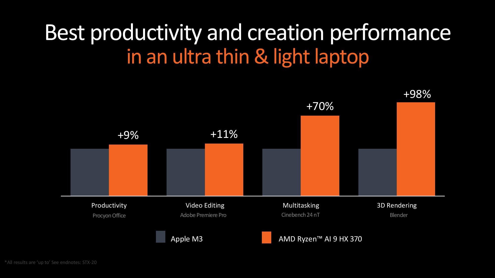
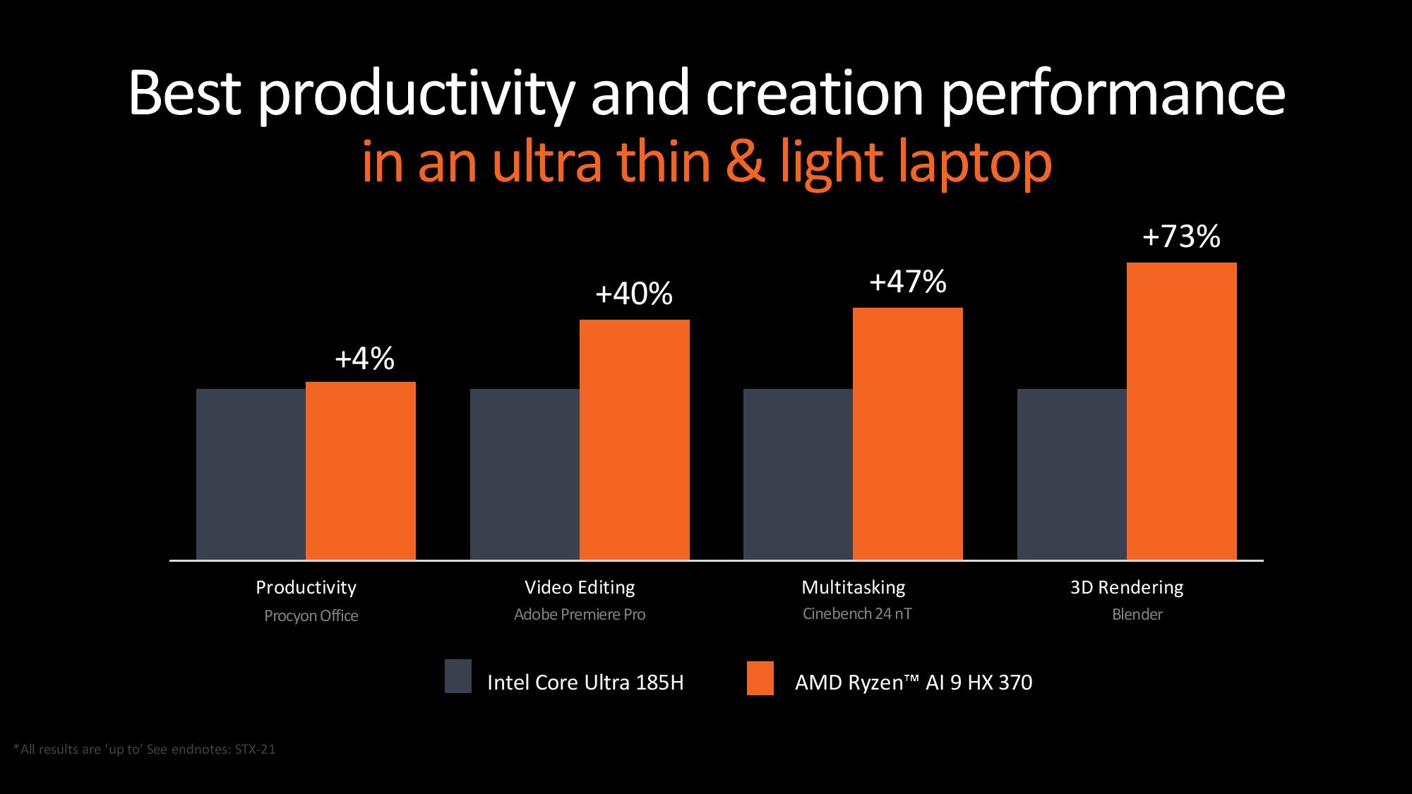
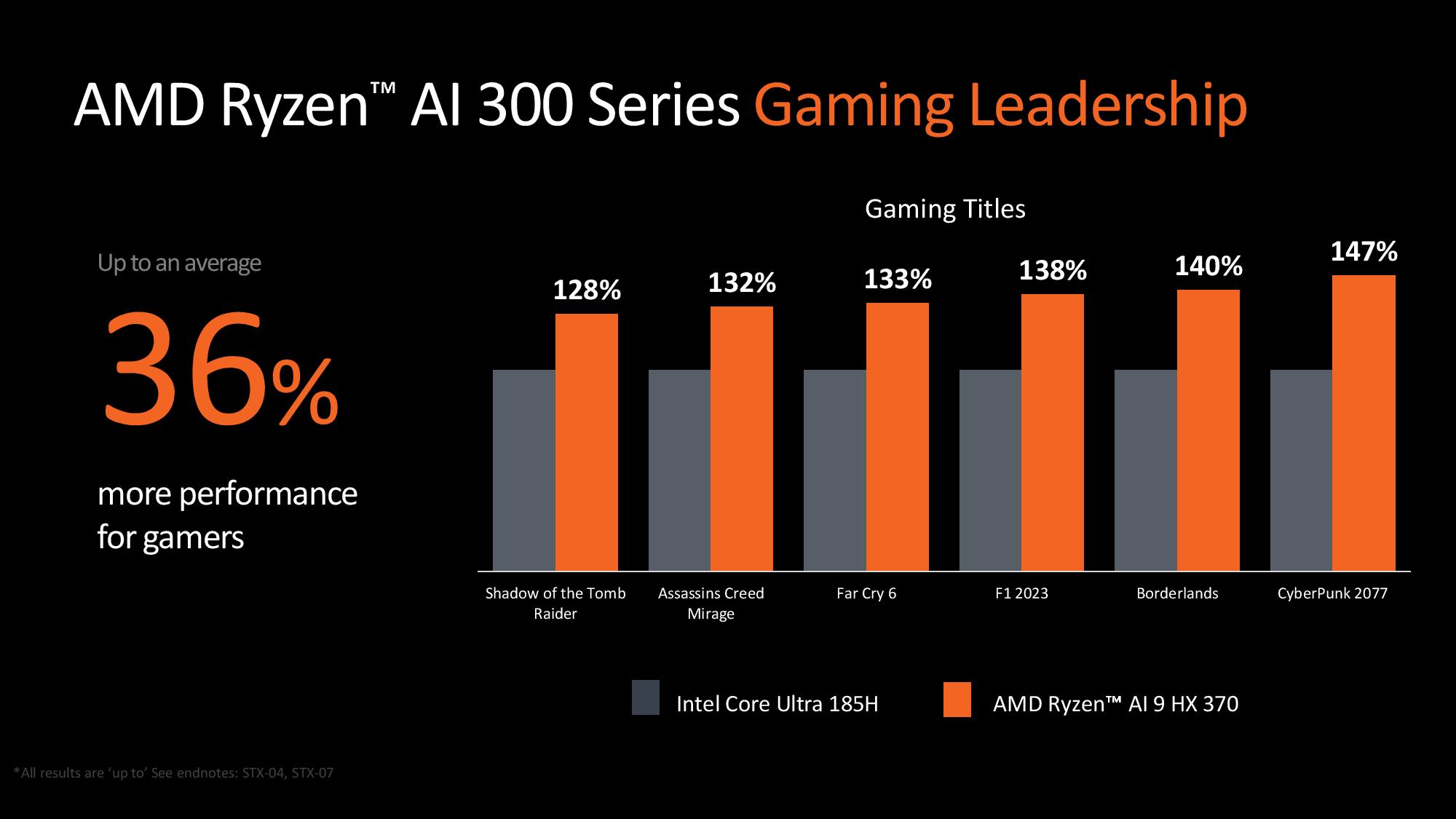
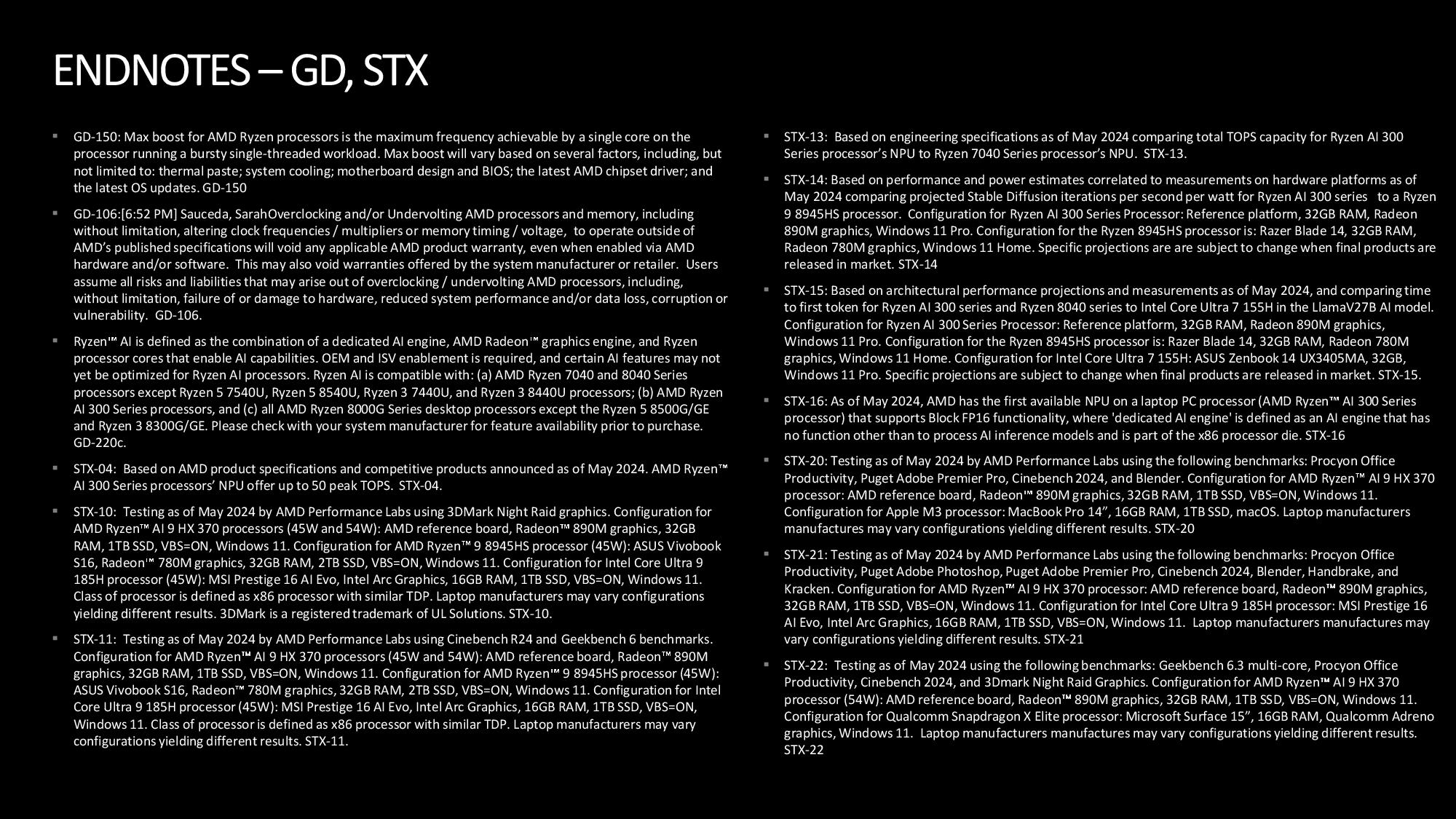
As with all vendor-provided benchmarks, AMD’s tests above should be taken with a grain of salt. We’ve also included the test notes at the end of the album.
AMD claims a 5X performance advantage with LLM models over shipping mobile processors in the market today, but notably, the yet-to-be-released 45 TOPS Qualcomm X Elite and 48 TOPS Lunar Lake aren’t included in these benchmarks.
AMD compared to Qualcomm’s publicly posted benchmark data in productivity work, though, claiming anywhere from a 5% advantage in responsiveness to a 10% advantage in productivity workloads with the Ryzen AI 9 HX 370. The company also threw in a whopping 60% performance advantage in graphics performance to underline its gaming chops. Apple’s M3 also makes an appearance, with AMD claiming a 9% advantage in productivity, an 11% advantage in video editing, and a 98% advantage in 3D rendering.
As you would expect, Intel’s Core Ultra 185H also appears in AMD’s benchmark roster, with AMD claiming a 4% lead in productivity workloads, a 40% gain in video editing, and a 73% advantage in 3D rendering. AMD also claims a 36% iGPU performance advantage over the Core Ultra 185H across a spate of titles.
Intel’s upcoming Lunar Lake processors would make an interesting comparison point here, but those haven’t been officially announced yet.
Thoughts
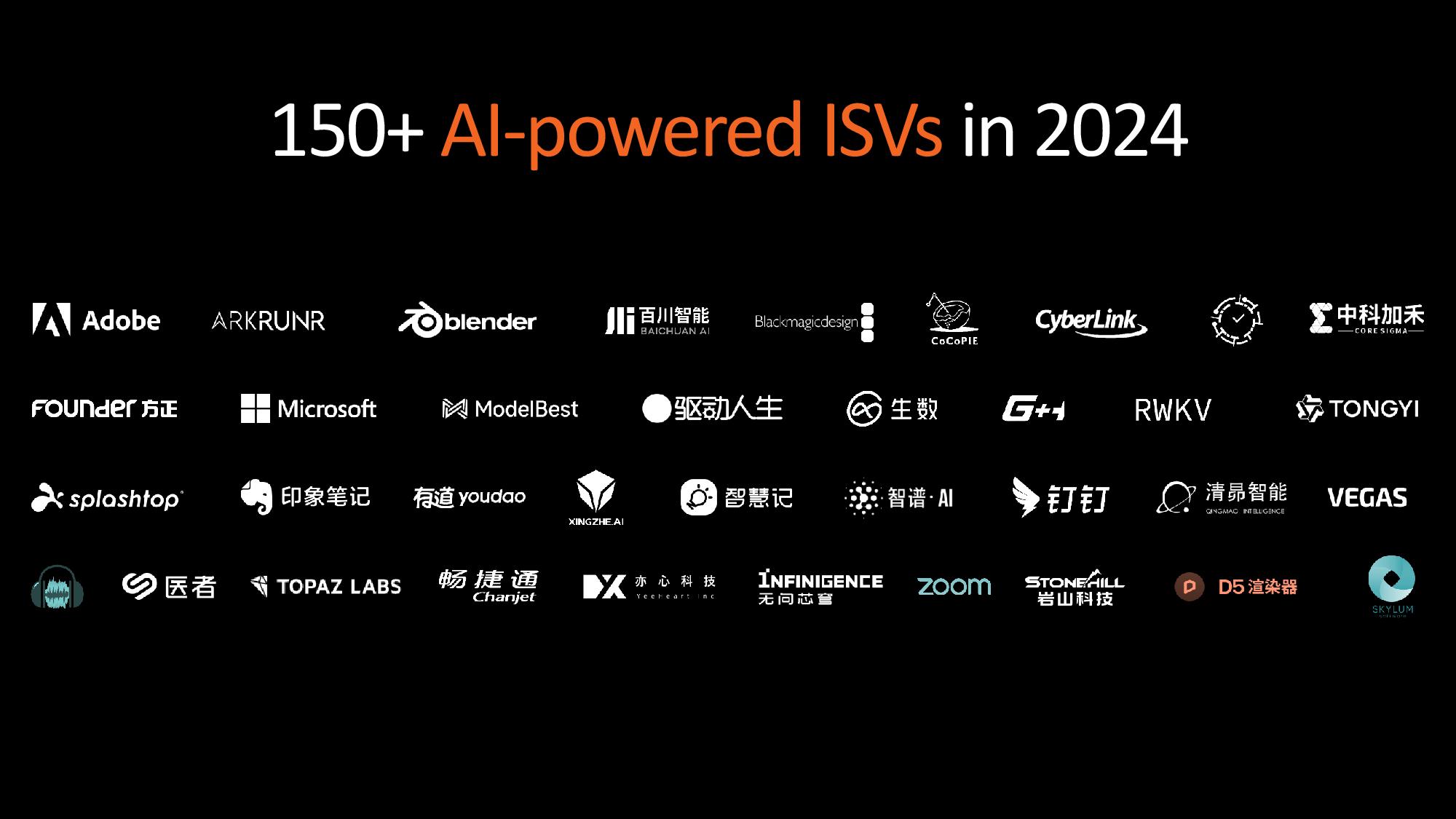
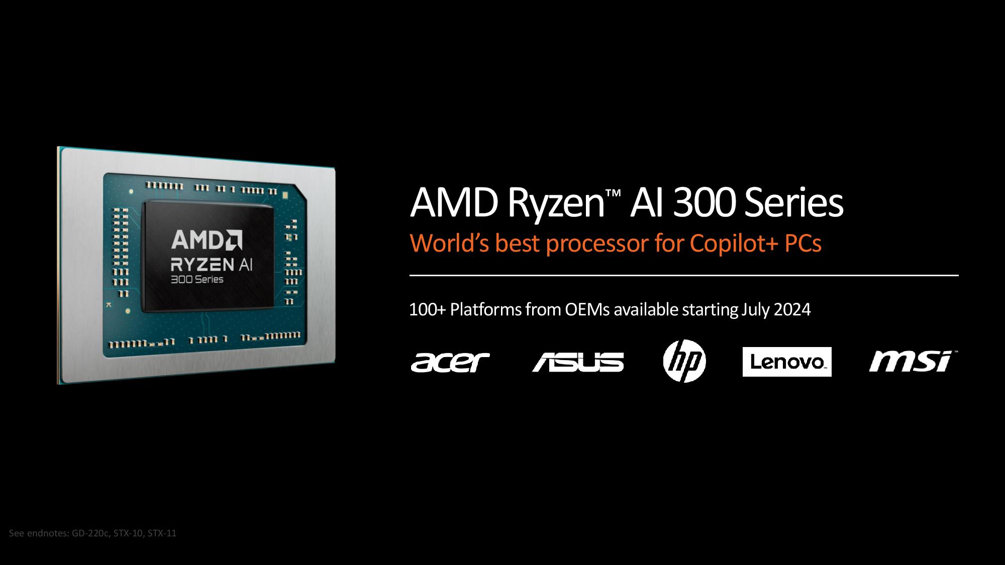
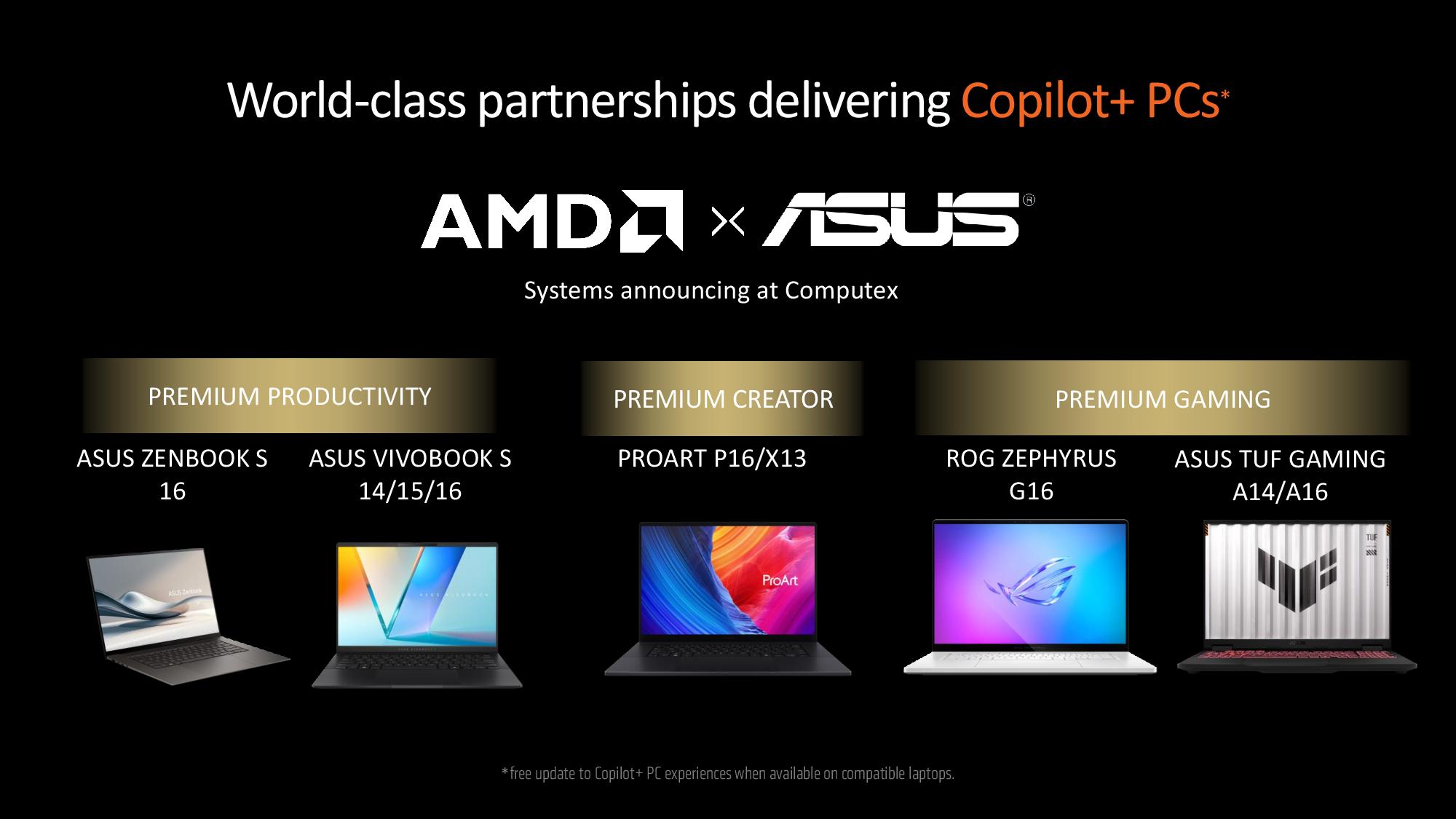
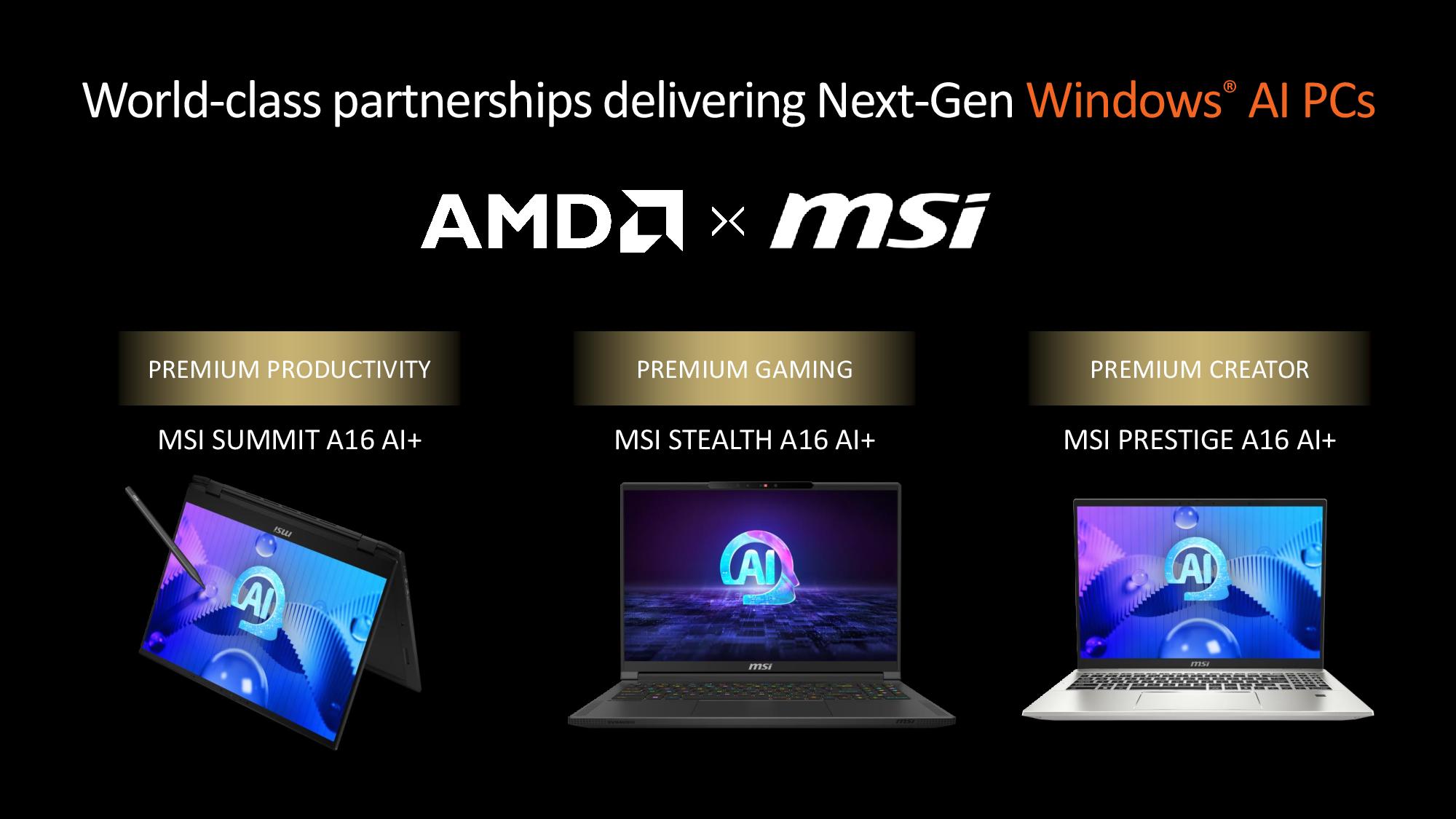
AMD has a full roster of developers with ISVs working with it to enable AI features, with plans for over 150 partners in 2024. The company also has a strong roster of hardware partners, with 100+ platforms starting to arrive next month. That includes many of the usual suspects, like Asus and MSI, both of which have multiple models on display here at Computex 2024.
AMD’s decision to bring its density-optimized Zen 5c cores to its top-tier Ryzen 9 lineup enables it to pack in more compute power in a smaller area of the chip, thus leaving room for a vastly expanded iGPU and NPU, both of which will pay dividends in other facets, like gaming and AI. With the performance benefits of the full-fat Zen 5 cores also under the hood along with a new faster, more efficient process node, the Ryzen AI 300 series chips look to be exceptionally competitive with Intel, Qualcomm, and Apple’s chips, setting the stage for a very competitive 2024 in the mobile market. Now, all that’s left is to see the chips in third-party benchmarks. With the arrival slated for July 2024, we won’t have to wait long to see how these chips stack up.

Paul Alcorn is the Editor-in-Chief for Tom's Hardware US. He also writes news and reviews on CPUs, storage, and enterprise hardware.
-
Notton Oh look, it turns out all the rumors were trueReply
300, so it's 100 more than Intel's 200
New naming scheme, but mixed into the older naming scheme
yay:rolleyes: -
cknobman We dont have AI, its the biggest scam there is.Reply
We have algorithms that learn what we teach them, then can either repeat or formulate responses based on what we teach it it.
It mimics patterns.
True AI would be able to make decisions on what its begin taught. AI would be able to decide for itself if what it is being taught is right or wrong, correct or incorrect.
Right now you can "teach" AI whatever you want because its not intelligent, its just a pattern recognizer and repeater. -
peachpuff Reply
Don't be such a party pooper... googles ai is telling you to put glue on your pizza so you better put it on your pizza!cknobman said:
True AI would be able to make decisions on what its begin taught. AI would be able to decide for itself if what it is being taught is right or wrong, correct or incorrect. -
genz Reply
Alright.cknobman said:We dont have AI, its the biggest scam there is.
We have algorithms that learn what we teach them, then can either repeat or formulate responses based on what we teach it it.
It mimics patterns.
True AI would be able to make decisions on what its begin taught. AI would be able to decide for itself if what it is being taught is right or wrong, correct or incorrect.
Right now you can "teach" AI whatever you want because its not intelligent, its just a pattern recognizer and repeater.
So how are we able to make decisions on what we were taught without past experience, self-taught or transferred?
People forget how much of human intelligence isn't actually there when we are born. -
KnightShadey Replycknobman said:We dont have AI, its the biggest scam there is.
Next thing you're gonna tell us is that AR & VR Aren't REAL !! 😱 🤯
Would calling it something like an "Algorithmic Inferencing' machine help you with the PR Marketing bits they use for selling it to the plebes ? 🤨 😜
PS, wait 'til ya' find out there's no actual Thunder in Thunderbolt hardware. 🤪 -
KnightShadey ReplyAdmin said:AMD unwrapped its new Ryzen AI 300 series, codenamed Strix Point, today at Computex... ..AMD’s new XDNA 2 engine that enables running AI workloads locally.
While it's a nice bump and promising (especially the option for 3 discrete workloads across CPU/NPU + iGPU + dGPU), it would've been far more impressive if the true 9 series HX platforms had been showcased with proper memory sized and better GPU option (with more VRAM). Especially since 12/24 still likely loses in most work/workstation scenarios to the 7945HX's 16/32 , which also didn't get a refresh when the 8040 series came out.
However, it should give us an idea of how Strix Halo could do with twice the memory bandwidth and 2.5x the CUs plus add 32MB local MALL cache (might help make up for PCie 4 vs 5) as a starting point... all before putting a capable GPU in there.
321 total TOPs for an R9 AI 370 HX + nV 4070 is OK , but as they say... twice (or thrice) as much for twice the price is Real Nice. 😎
Entertaining that ASUS early launch material highlights "45 TOPS NPU" for it's TUF A16 platform instead of 50....
ibb (dot) co/7NmV53V
Did that evolve since they put that slide together or just a Qualcomm type Typo? 🧐 -
bit_user Reply
My guess is that it's basically like texture compression. I've heard of mobile NPUs using compression on the weights, but not really seen AMD or Nvidia talk about it (other than handling a limited degree of sparseness). It always seemed to me like a natural thing for GPUs to do, given their texture units are already in the datapath and already have hardware support for texture compression. ...except this isn't a GPU!The article said:Block BF16, a new data format that provides the full accuracy of FP16 with many of the same compute and memory characteristics of INT8. AMD says Block FP16 is plug-and-play; it doesn’t require quantizing, tuning, or retraining the existing models.
No. ...I'm 99.9% sure it's not.The article said:It isn’t yet clear if Block FP16 is certified as an IEEE standard.
But, that's irrelevant if it's basically invisible to software, as they claim. The main reason for IEEE standards is to have some consistency between hardware implementations, so that software doesn't have to introduce a ton of special cases, one for each hardware implementation. -
JayNor "AMD hasn’t yet shared the full TOPS rating for its chips with the CPU and GPU added in."Reply
why not? -
KnightShadey Replybit_user said:My guess is that it's basically like texture compression. I've heard of mobile NPUs using compression on the weights, but not really seen AMD or Nvidia talk about it (other than handling a limited degree of sparseness). It always seemed to me like a natural thing for GPUs to do, given their texture units are already in the datapath and already have hardware support for texture compression. ...except this isn't a GPU!
No. ...I'm 99.9% sure it's not.
But, that's irrelevant if it's basically invisible to software, as they claim. The main reason for IEEE standards is to have some consistency between hardware implementations, so that software doesn't have to introduce a ton of special cases, for each hardware implementation.
Yeah, could be, but I'm doubtful because it seems like a stumbling block scaling size & speed long term.
I got the feeling it was more like how BFloat16 (the other B16 🤓 ) deals with FP32 for rounding up/down, so it just becomes an 'efficient'/elegant math work around, that can be used in any scenario, rather than adding silicon for de/compression, but that's just my take/guess on it.
It's something I wish they spent more time on, but I suspect we'll get that in the deep dives in the coming day/weeks before launch.
My initial read on it was to react "OH, this is how AMD is going to react to not having intel's AVX FP16 support" which of course is helpful for Ai workloads.
Who knows it may be the best of both worlds giving them speed down low for consumer Ai applications/platforms, which are definitely more about doing 95% of the job in 1/3 the time rather than speed up the full-fat FP16/32 by 20-50% (usually closer to 10% because at that level you are still heavily memory bound/restricted ). 🤔🤷🏻♂️
Too me BFP16 like adding a small turbo to a small engine in a light sports car (Lotus 7) .... boom huge impact , while FP16 is like adding another turbo to a Chiron... OK, improvement, but not dramatic, and not where the majority of the market will be for Copilot+ level Ai PCs for the next coupla years.
The more precise faster seems like still the domain of commercial applications.... (where dedicated racks of precision are still telling people to eat rocks 🥸 🤣 ).
Now if only Block FP16 were as exciting as the French movie District BF13. 🤡
(* after reading your other post in the other thread, I think I added too many unnecessary analogies and aphorisms, when you likely would've been fine with just half the words in the second paragraph. THG has definitely added more depth in the forums since I left over a decade ago. Wish there were more deep-dive folks then. Now... to try and curb the dad humour.... must resist. 🥸 😉 )
