ASML sets new EUV chipmaking density record, proposes Hyper-NA tools and radical EUV speed boosts
Smaller, faster transistors at unprecedented speed.
ASML announced at imec’s ITF World 2024 conference that it has now set a new chipmaking density record with its first High-NA machine, surpassing a record it set just two months ago. ASML‘s former President and CTO, Martin van den Brink, who now serves in an advisory role at the company, also proposed that the company could develop a Hyper-NA chipmaking tool to deliver further scaling beyond its High-NA machine and shared potential roadmaps. He outlined a plan to reduce EUV chipmaking costs by radically boosting the speed of future ASML tools to 400 to 500 wafers per hour (wph), more than double the current peak of 200 wph. He proposed a modular unifying design for ASML’s future families of EUV tools as well.
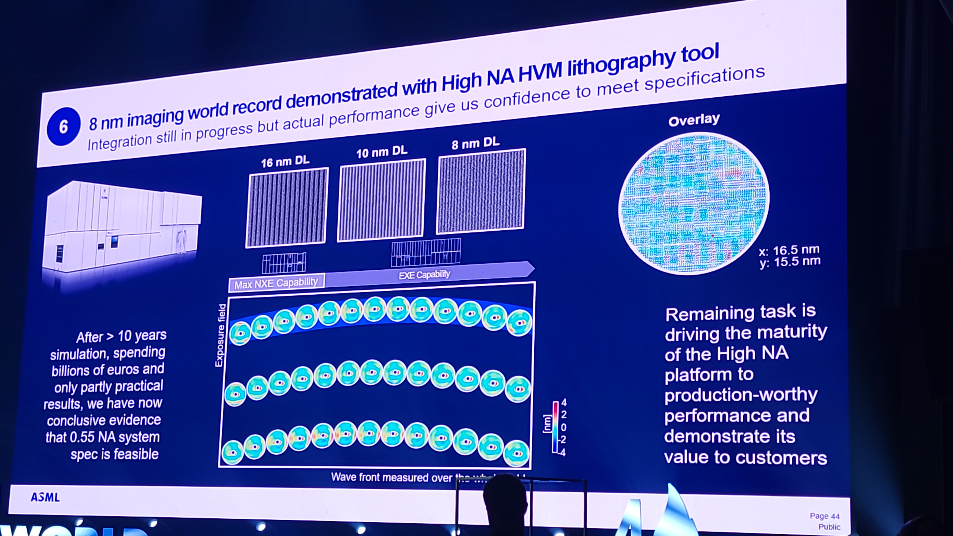
Van der Brink said that, after further tuning, ASML has now printed 8nm dense lines with its pathfinding High-NA EUV machine—a density record for a machine designed for production environments. This beats the company’s own record it set in early April when it announced it had printed 10nm dense lines with its pathfinding High-NA machine located in its joint lab with imec at ASML's Veldhoven, Netherlands headquarters.
For perspective, ASML’s standard Low-NA EUV machines can print critical dimensions (CD—the smallest feature that can be printed) of 13.5nm, and the new High-NA EXE:5200 EUV tool is designed to create even smaller transistors by printing 8nm features. As such, ASML has now demonstrated that its machine can meet its basic specifications.
“Today we have made progress to the point that we are able to show record imaging down to 8nm being corrected over the full field, but also having some level of overlay,” Van der Brink said, “This is not perfect data, by the way, but it is just to show you the progress. We are confident today that where we are with High-NA, that we will be able to cross this to the finish line in the coming time."
The milestone represents the culmination of more than 10 years of R&D and billions of Euros of investment, but more work remains to be done to optimize the system and ready the technology for mass production at major chipmakers. That work is already underway in the Netherlands, while Intel, the only chipmaker that’s known to have a High-NA system already fully assembled, is following closely in ASML’s footsteps as it brings its own machine into operation at its D1X fab in Oregon. Intel will use its EXE:5200 High-NA machine for R&D purposes at first, and then press it into production for its 14A node.
Van der Brink also proposed a new Hyper-NA EUV machine once again, but no final decision on the machine has been made — It appears ASML is gauging industry interest, but only time will tell if it comes to fruition.
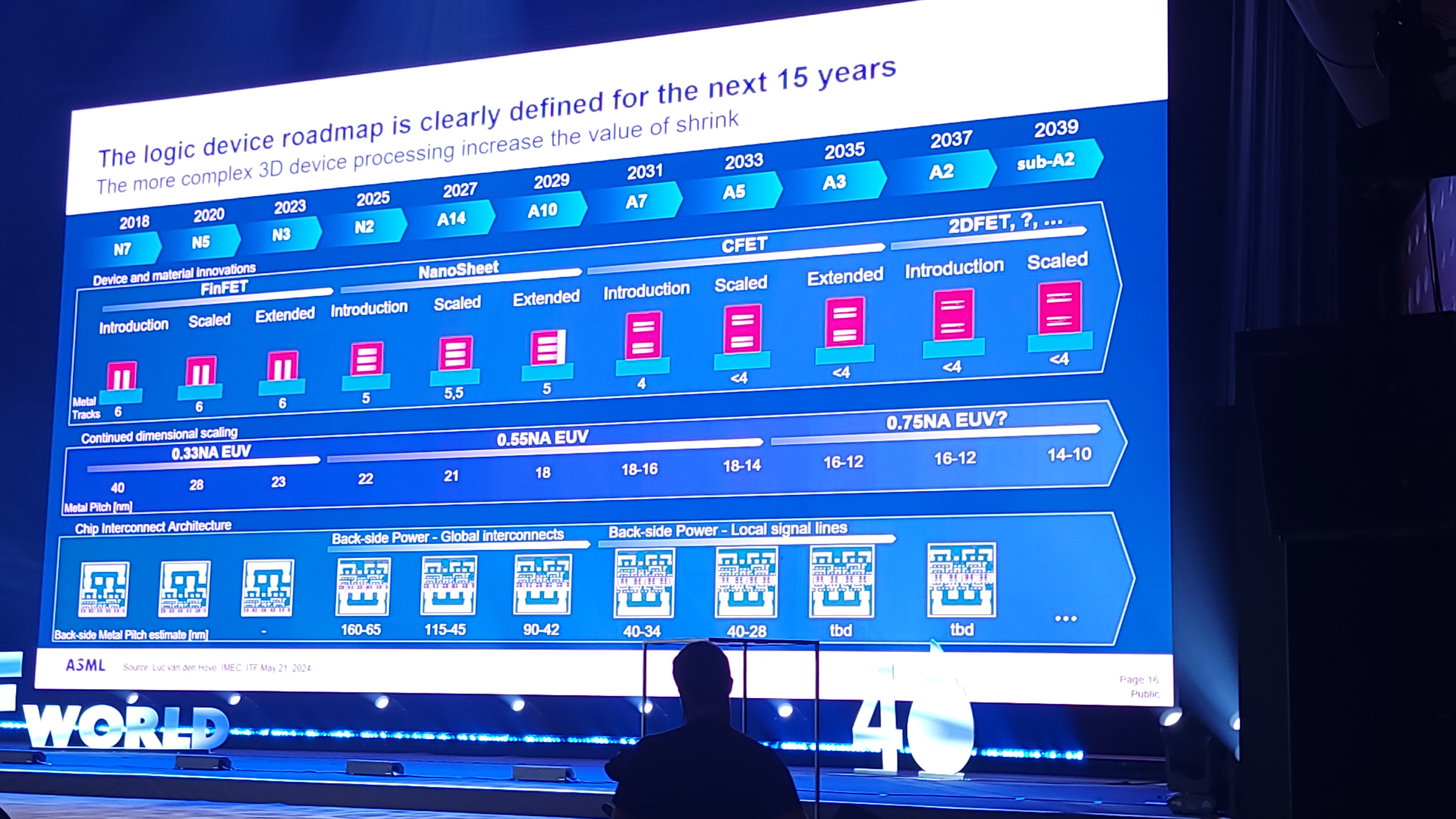
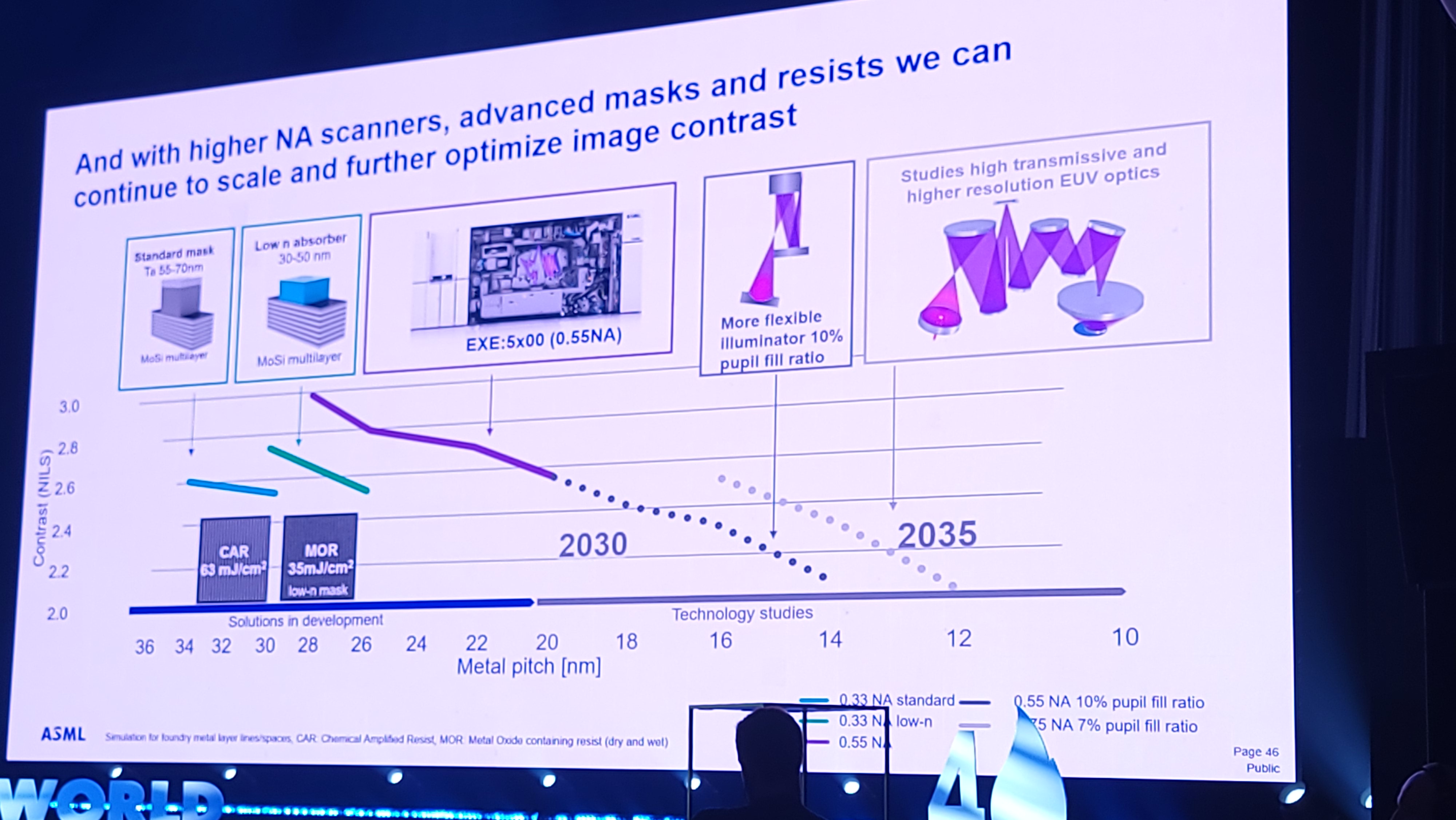
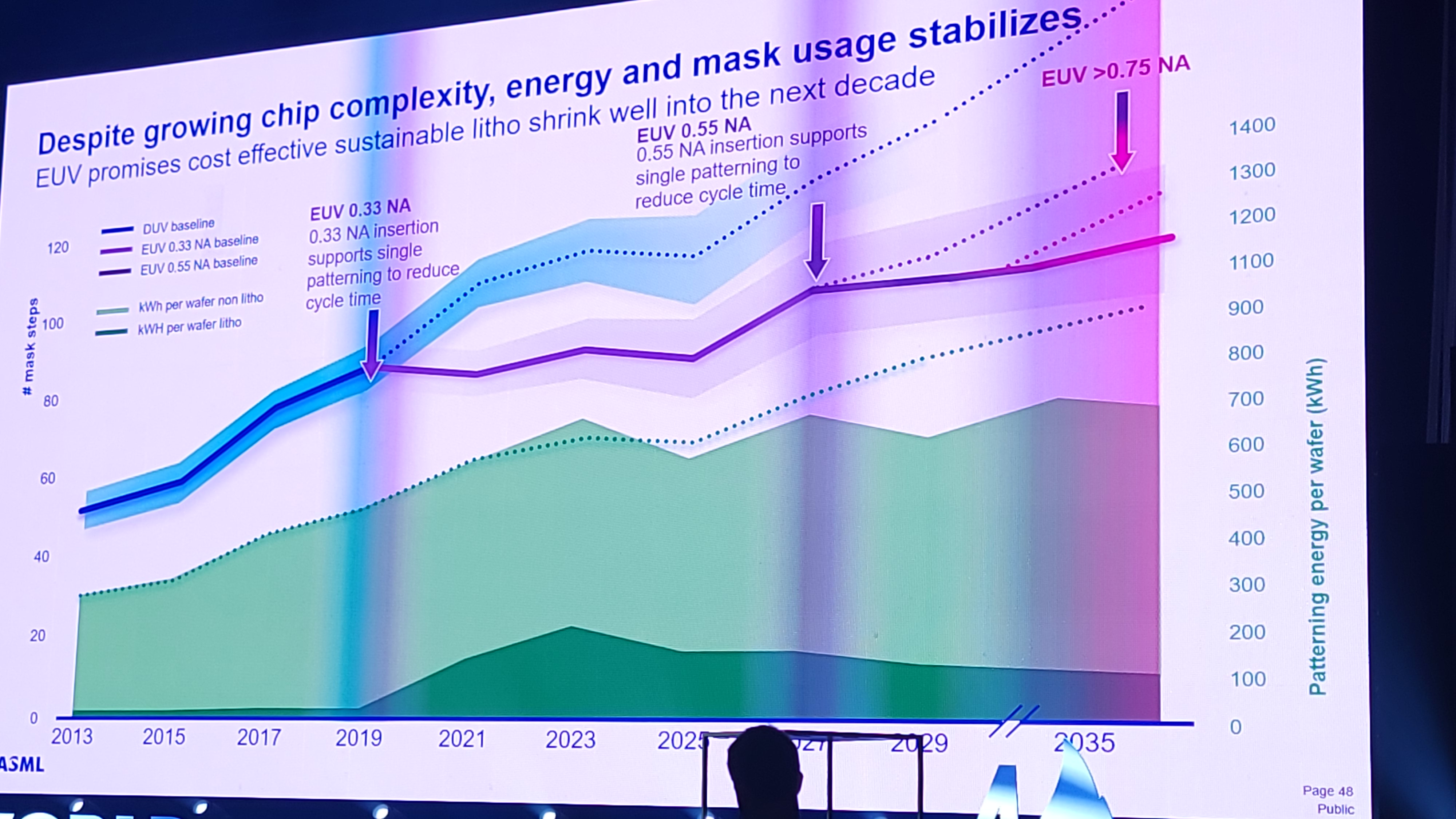
Today’s standard EUV machine uses light with a 13.5nm wavelength and a 0.33 numerical aperture (NA—a measure of the ability to collect and focus light). In contrast, the new High-NA machines use the same light wavelength but employ a 0.55 NA to enable printing smaller features. Van der Brink’s proposed Hyper-NA system would use the same wavelength of light again but widen the NA to 0.75 to enable printing even smaller features. We aren't sure of the proposed critical dimension, but ASML's transistor timeline above shows it is intercepting at 16nm metal pitches (A3 nodes) and extending to 10nm (sub-A2 nodes).
According to the roadmap above, Hyper-NA could be feasible for single-exposure 2DFET transistors, but it isn't clear if using High-NA with multi-patterning could also create such fine pitches.
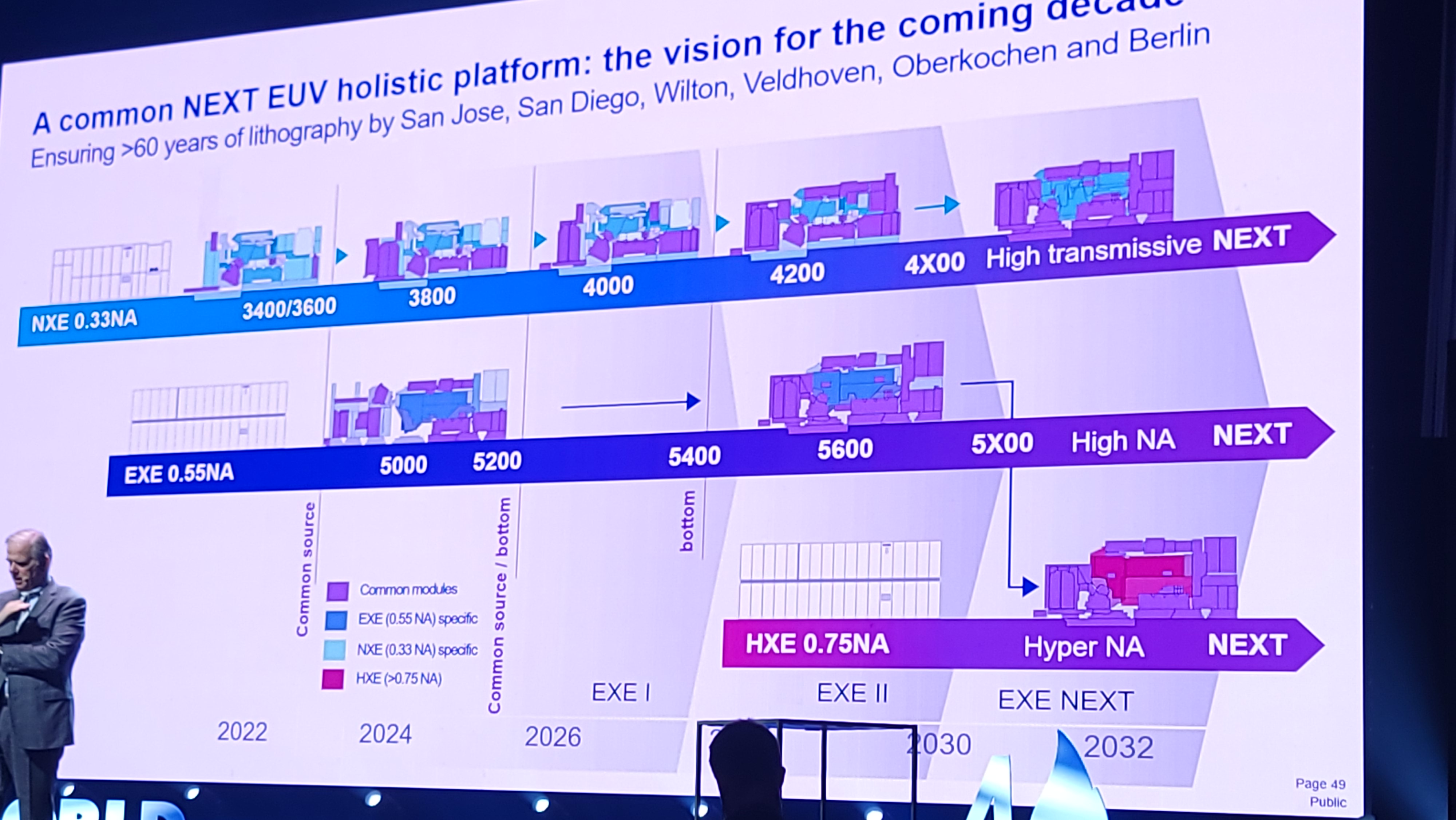
As you can see in the first slide above, this machine wouldn’t come until ~2033. Today’s High-NA machines already cost around $400 million. Hyper-NA would be a more expensive option due to the need for larger and more advanced mirrors and an improved illuminator system.
As with its predecessors, the goal of Hyper-NA is to enable printing smaller features with a single exposure to avoid multi-patterning techniques (multiple exposures of the same region) that tend to add time and steps to the chipmaking process while also increasing the chance of defects, all of which conspires to increase costs. Van Der Brink said that continued development work on resists and advanced masks would be key to improving the resolution of printed features. Hyper-NA would also use an improved illumination system for optimum results. ASML didn't elaborate, but It's logical to think the improved illuminator would pair with a higher-power light source to help increase the dose to both offset the higher mirror angles used for 0.75 NA and to improve throughput.
Van der Brink also proposed increasing the throughput of the company’s future machines from ~200 wph today to 400 to 500 wph in the future. This is another lever that ASML can pull to reign in costs, thus combatting the increasing price per transistor trend with each new generation of chips.
To speed development and reduce costs, ASML already uses its existing Low-NA Twinscan NXE:3600 EUV machines as a building block for its new High-NA machine. ASML's Low-NA models have a modular design that allows the company to leverage proven technology and modules for its new tools, and the company only adds new modules where needed.
However, there’s room for much more optimization. Van der Brink sees the company doubling down on the modular design philosophy as it creates new tools over the coming decade. The proposed long-term roadmap shows Low-NA, High-NA, and Hyper-NA all having an increasingly common modular platform with shared components. This design is yet another lever that ASML could pull to rein in costs.
The chip industry appears to have a solid runway for future development through Gate-All-Around (GAA) and complementary field-effect transistors (CFETs) built with Low-NA and High-NA tools, but aside from Hyper-NA, no real candidate has stepped forward to potentially enable future generations of process node technologies. As always, cost will be the key factor, but ASML is obviously already thinking of ways it can make the Hyper-NA pricing equation more attractive to its customers.
Get Tom's Hardware's best news and in-depth reviews, straight to your inbox.

Paul Alcorn is the Editor-in-Chief for Tom's Hardware US. He also writes news and reviews on CPUs, storage, and enterprise hardware.
-
bit_user Reply
@PaulAlcorn , I've recently noticed this in another article, on here (possibly written by Anton? I forget), that Imec is being written in all lower case letters. I wondered why, given that it's a proper noun. When I visit their web site, I see they capitalize it, in their own articles.The article said:ASML announced at imec’s ITF World 2024 conference ...
https://www.imec-int.com/en
Is it that you're trying to avoid confusion between I vs L? If that's the concern, maybe write it in a serif font, so it shows up like Imec. -
bit_user BTW, it's good to see ASML working on the issue of chip fabrication costs. It seems to me that further reducing the cost per transistor is almost a bigger challenge than actually increasing density!Reply -
Replybit_user said:@PaulAlcorn , I've recently noticed this in another article, on here (possibly written by Anton? I forget), that Imec is being written in all lower case letters. I wondered why, given that it's a proper noun. When I visit their web site, I see they capitalize it, in their own articles.
https://www.imec-int.com/en
Is it that you're trying to avoid confusion between I vs L? If that's the concern, maybe write it in a serif font, so it shows up like Imec.
Both contexts are sometimes used, btw. I have seen the company and few other websites spell it as 'imec" in the middle of sentences, "Imec" at the start of a sentence, and "IMEC" only in headlines.
This is more in line with the company's marketing strategy to match and "blend" with the brand's logo, which is in lowercase as well.
So basically, "imec" is the most commonly used name, as per my observation. One company rep echoed on this issue at a conference that they prefer using "imec" in akin to match the brand's logo, but there is no hard and fast rule to this.
https://www.spectroexpo.com/wp-content/uploads/2018/07/FINAL_imec_baseline.jpg
But, there have been some conflicting thoughts on this discussion before as well on the internet.
Some argue since this is an acronym, it should be IMEC, and it kind of makes sense. And a lowercase capitalization might look awkward, but as per Wikipedia styling standard (MoS) there shouldn't be much of an issue
But I have noticed several websites/secondary sources out there which refer to the company as both by either "Imec" or "imec". But mostly 'imec" in the middle of sentences, "Imec" at the start of a sentence.
Other websites on the other hand only prefer using 'imec" instead in lower case.
https://nnieuws.be/artikel/imec-vlaanderen-start-testen-met-voertuigen-die-telebediend-autonoom-rijden
Edit:
Btw, let Paul answer though. I was just giving my insight. -
bit_user Reply
Articles should prioritize clarity and not worry about how a brand chooses to stylize its logo. If it's an acronym or initialism, as you say, then I'd write it IMEC. For a reader unfamiliar with the organization, using all-lowercase seems like it'd be very confusing.Metal Messiah. said:This is more in line with the company's marketing strategy to match and "blend" with the brand's logo, which is in lowercase as well. -
Yeah, I agree with you. IMEC would be better if used in any article or reference. IDK, but this company's name has lacked "uniformity" when it comes to standardization.Reply
-
Paul Alcorn Reply
Imec when it's the first word in a sentence, imec when it is not. You can see this if you head to the organization's PR page or if you receive any communication from them; this is the way they communicate to the world, so that is what we use. Much like SK hynix, for example.bit_user said:@PaulAlcorn , I've recently noticed this in another article, on here (possibly written by Anton? I forget), that Imec is being written in all lower case letters. I wondered why, given that it's a proper noun. When I visit their web site, I see they capitalize it, in their own articles.
https://www.imec-int.com/en
Is it that you're trying to avoid confusion between I vs L? If that's the concern, maybe write it in a serif font, so it shows up like Imec. -
bit_user Reply
Their practice sounds to me like the work of an overzealous marketing person, there. I see a distinction between logo and language, but apparently they don't.PaulAlcorn said:Imec when it's the first word in a sentence, imec when it is not. You can see this if you head to the organization's PR page or if you receive any communication from them; this is the way they communicate to the world, so that is what we use. Much like SK hynix, for example.
I think your position is defensible, even if it's not what I'd do. Thanks for replying.
: ) -
That's odd if they really took a page from SK HYNIX's book to set an example.Reply
IMEC if used as an acronym, would sound more acceptable, and less confusing in a broader context.
