Intel details Gaudi 3 at Vision 2024 — new AI accelerator sampling to partners now, volume production in Q3
GPUs fall by the wayside as Intel goes all-in on Gaudi for AI.
Intel made a slew of announcements during its Vision 2024 event today, including deep-dive details of its new Gaudi 3 AI processors, which it claims offer up to 1.7X the training performance, 50% better inference, and 40% better efficiency than Nvidia’s market-leading H100 processors, but for significantly less money. Intel also announced new branding for its data center CPU portfolio, with the Granite Rapids and Sierra Forest chips now branded as the new ‘Xeon 6’ family. Those chips are on track to come to market this year and add support for the new performance-boosting standardized MXFP4 data format, which you can read about here.
Intel also announced that it is developing an AI NIC ASIC for Ultra Ethernet Consortium-compliant networking and an AI NIC chiplet that will be used in its future XPU and Gaudi 3 processors while also being made available to external customers through Intel Foundry, but it didn’t share more details on these networking products.
Nvidia’s dominance in AI infrastructure and software is undisputed. Still, Intel, like AMD, is looking to carve out a position as the premier alternative to Nvidia as the industry continues to struggle with Nvidia's crushing AI GPU shortages. To that end, Intel also outlined the full breadth of its AI enablement programs, which stretch from hardware to software, as it looks to gain traction in the booming AI market that Nvidia and AMD currently dominate. Intel’s efforts focus on developing its partner ecosystem to deliver complete Gaudi 3 systems while also working to build an open enterprise software stack to serve as an alternative to Nvidia’s proprietary CUDA.
Intel provided deep-dive details of the Gaudi 3 architecture along with plenty of convincing benchmarks against existing Nvidia H100 GPUs (data for the upcoming Blackwell systems isn’t available yet). First, let’s take a closer look at the Gaudi 3 architecture.
Intel Gaudi 3 Specifications
Intel’s Gaudi 3 marks the third generation of the Gaudi accelerator, which was the fruit of Intel’s $2 billion acquisition of Habana Labs in 2019. The Gaudi accelerators will enter high-volume production and general availability in Q3 of 2024 in OEM systems. Intel will also make Gaudi 3 systems available in its Developer Cloud, thus providing a fast on-ramp for prospective customers to test the chips.
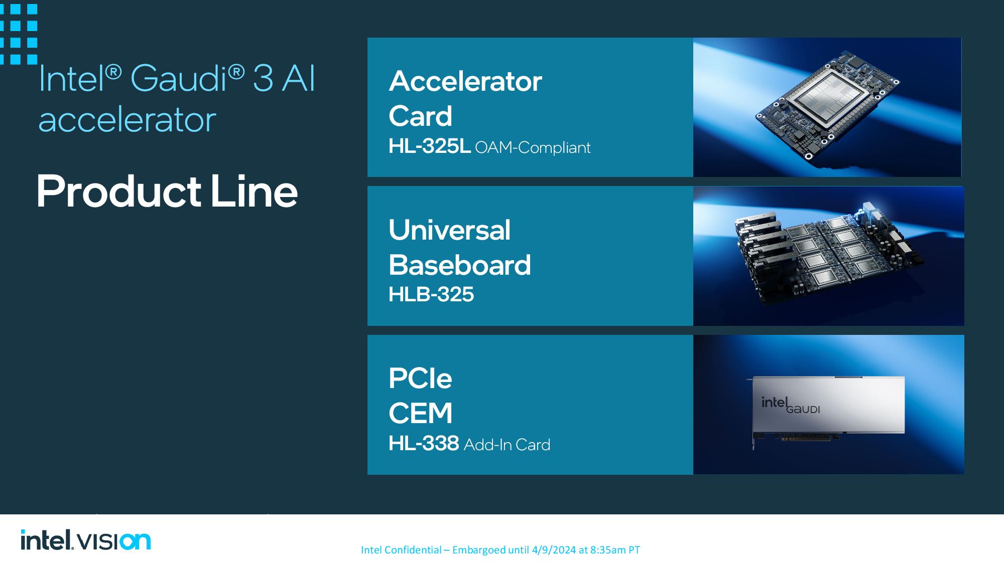
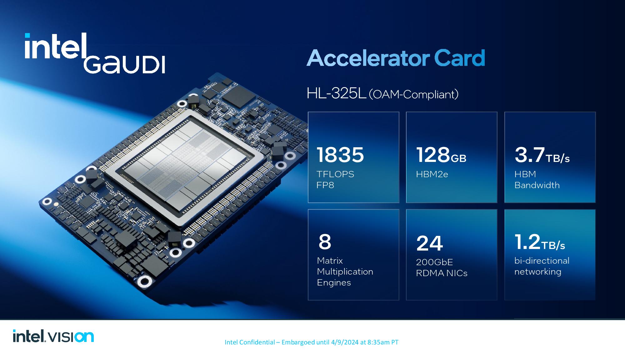

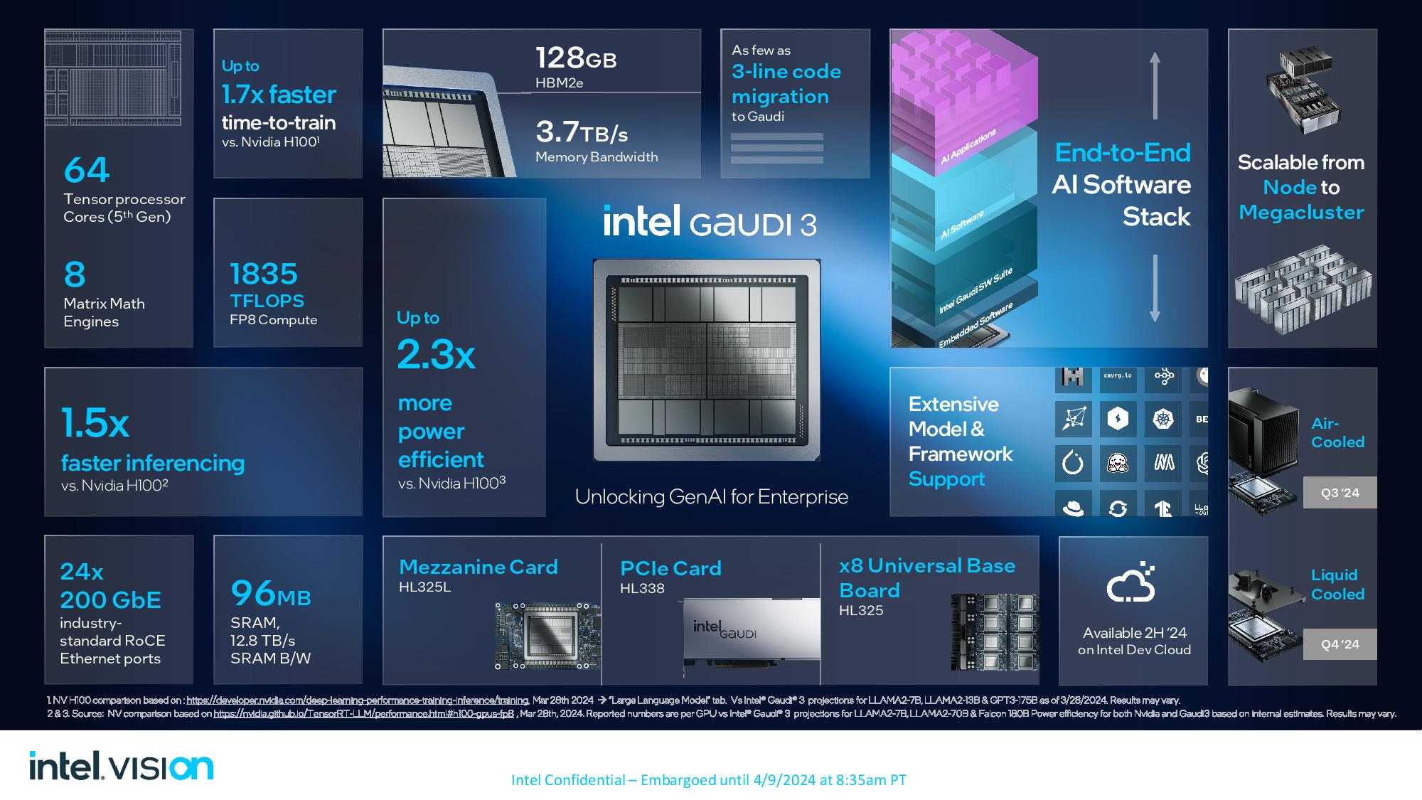

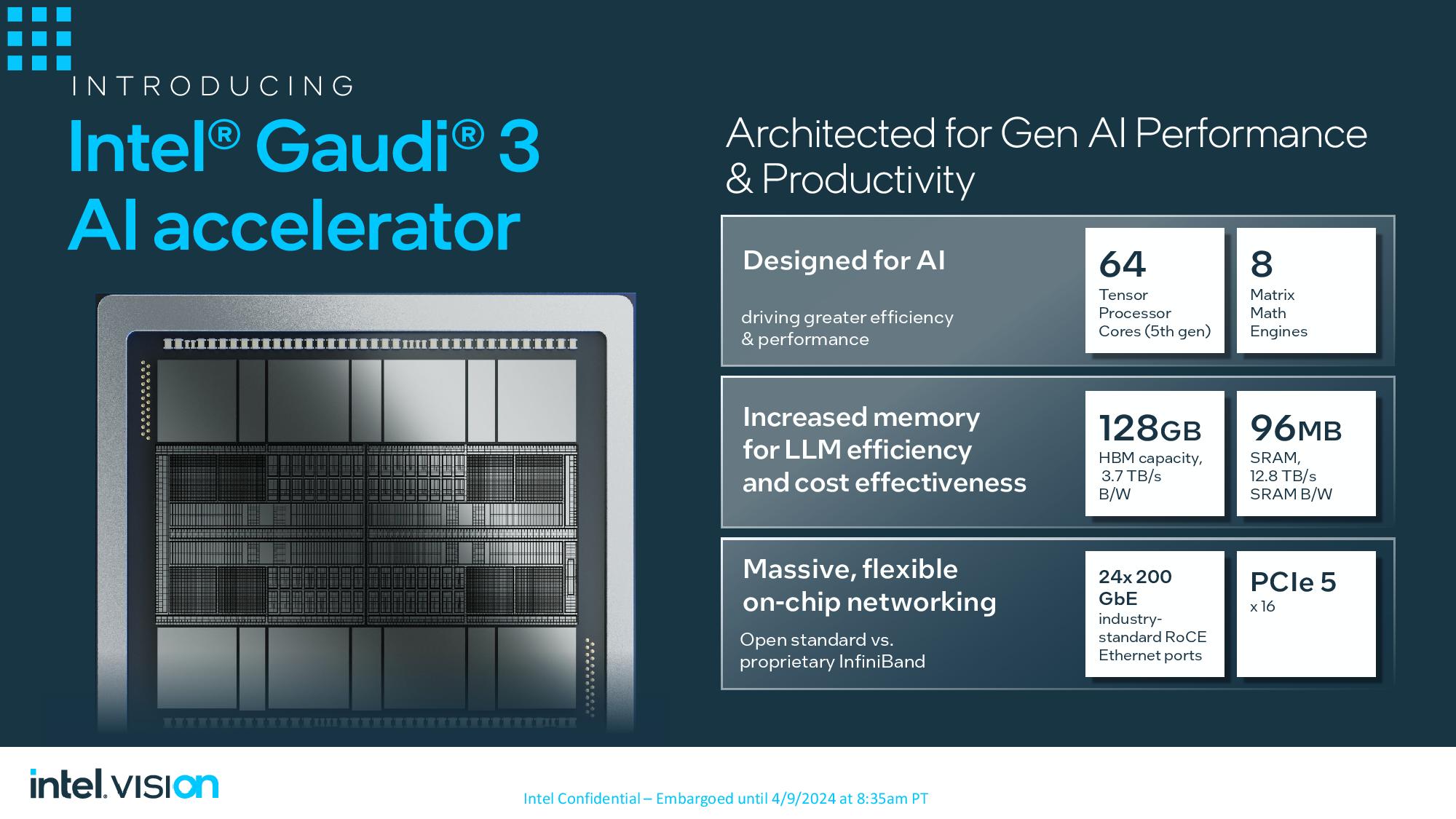
Gaudi comes in two form factors, with the OAM (OCP Accelerator Module) HL-325L being the common mezzanine form factor found in high-performance GPU-based systems. This accelerator has 128GB of HBM2e (not HBM3E), providing 3.7 TB/s of bandwidth. It also has twenty-four 200 Gbps Ethernet RDMA NICs. The HL-325L OAM module has a 900W TDP (higher TDPs are possible, ostensibly with liquid cooling) and is rated for 1,835 TFLOPS of FP8 performance. The OAMs are deployed in groups of eight per server node and can then scale up to 1,024 nodes.
Intel claims Gaudi 3 provides twice the FP8 and four times more BF16 performance than the prior generation, along with twice the network bandwidth and 1.5X the memory bandwidth.
Get Tom's Hardware's best news and in-depth reviews, straight to your inbox.
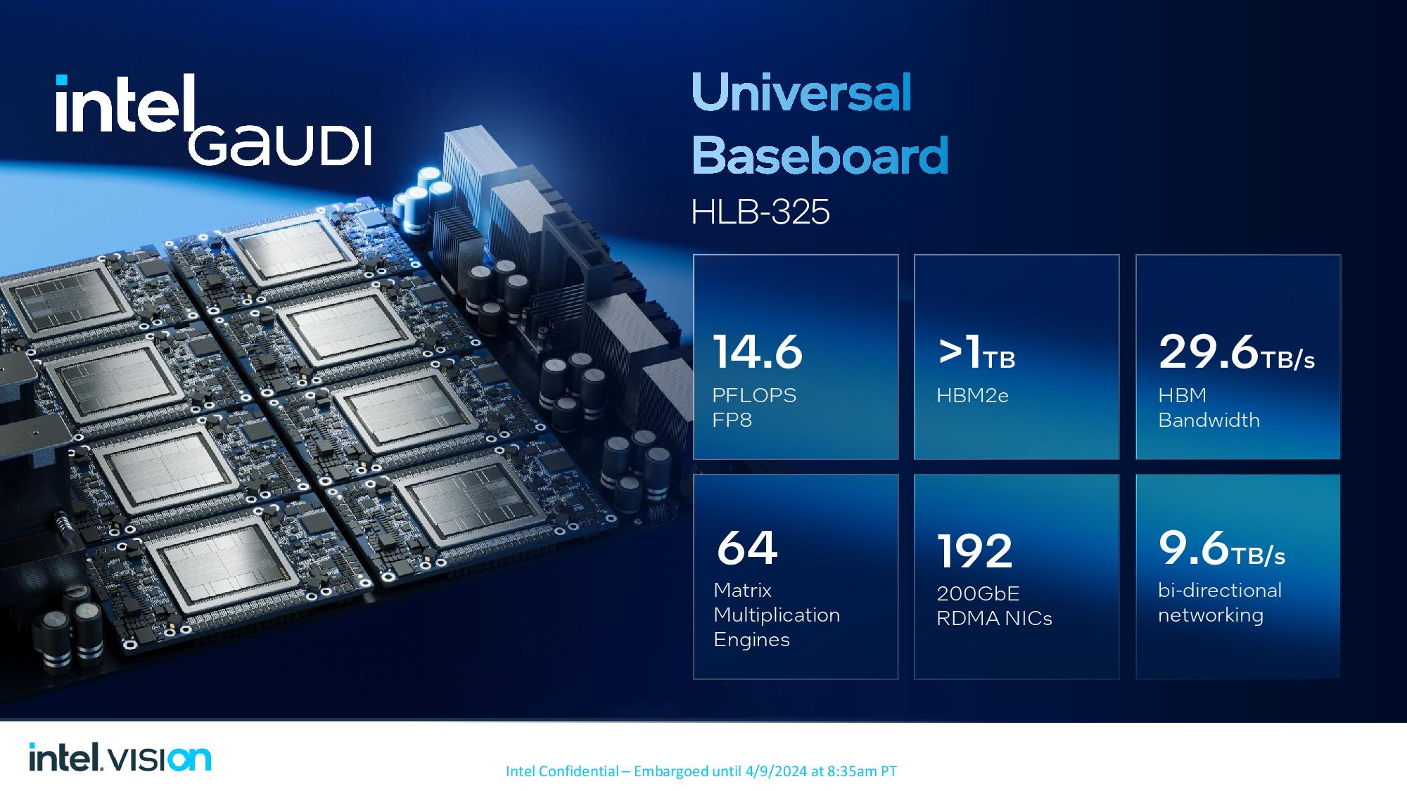
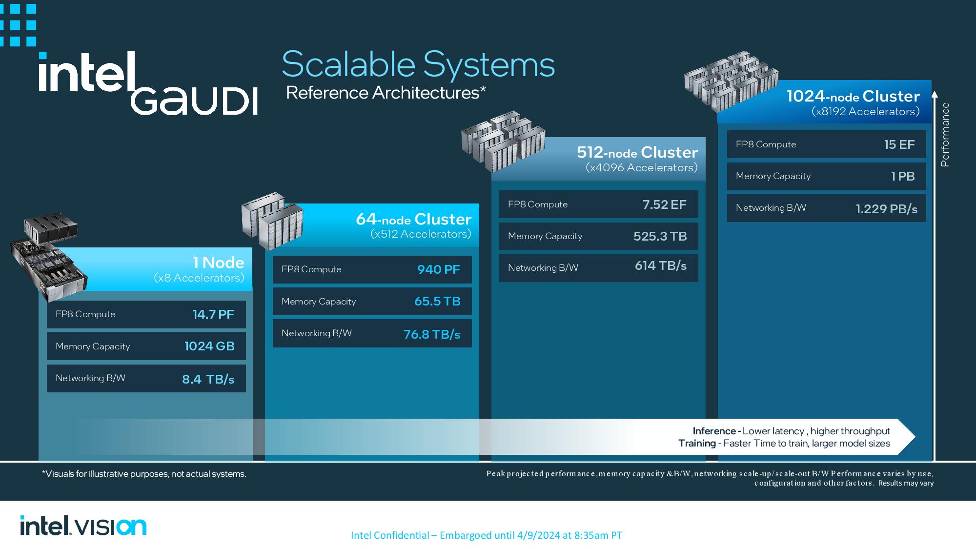
The OAMs drop into a universal baseboard that houses eight OAMs. Intel has already shipped OAMs and baseboards to its partners as it prepares for general availability later this year. Scaling to eight OAMs on the HLB-325 baseboard brings performance to 14.6 PFLOPS of FP8, while all other metrics, such as memory capacity and bandwidth, scale linearly.
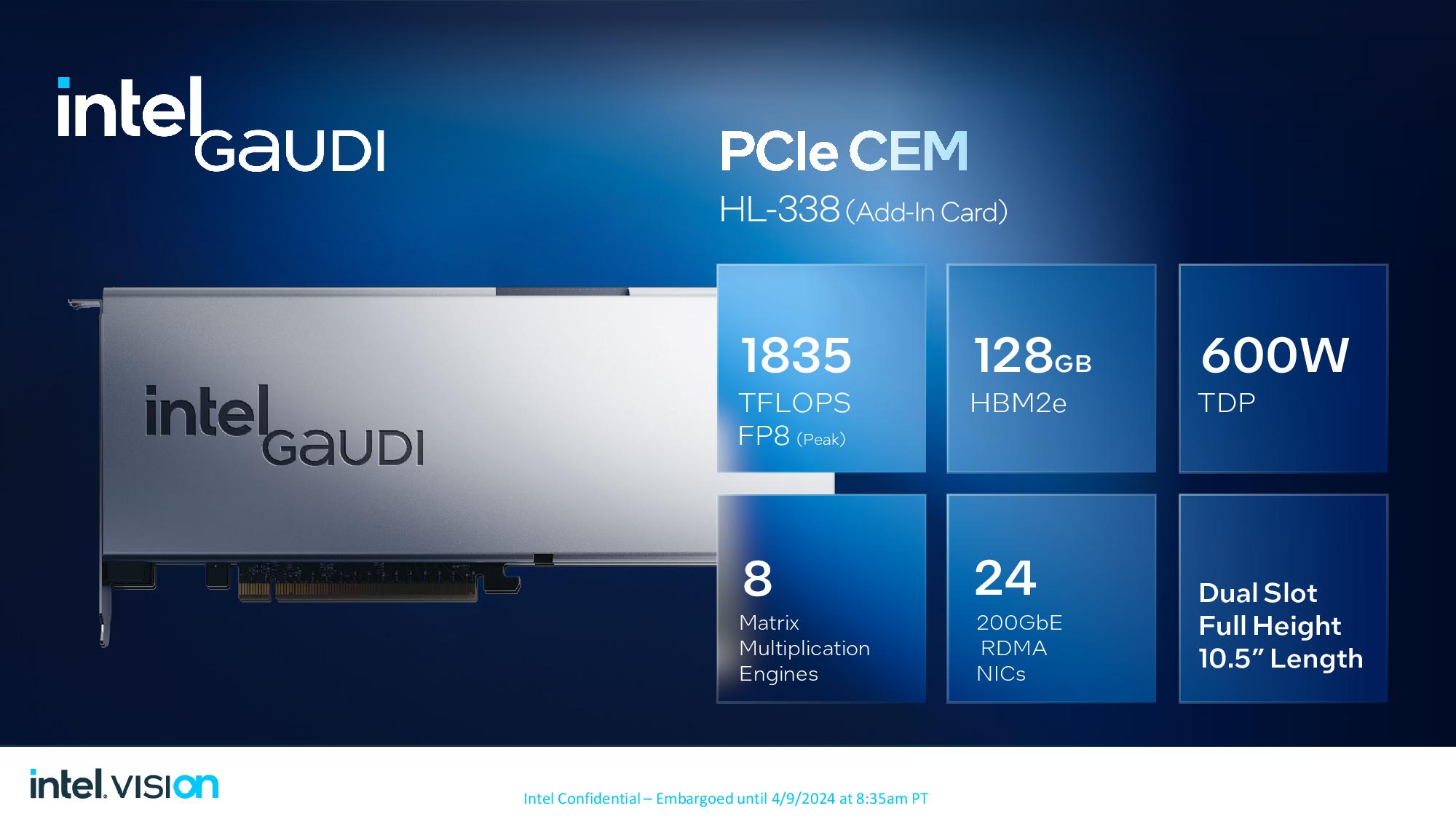
Intel has a Gaudi 3 PCIe dual-slot add-in card with a 600W TDP as well. This card also has 128GB of HBMeE and twenty-four 200 Gbps Ethernet NICs — Intel says dual 400 Gbps NICs are used for scale-out. Intel says the PCIe card has the same peak 1,835 TFLOPS of FP8 performance as the OAM, which is interesting given its 300W lower TDP (this likely won't hold in long-duration workloads). However, scaling is more limited inside the box, as it is designed to work in groups of four. Intel says this card can also scale out to create larger clusters but didn’t provide details.
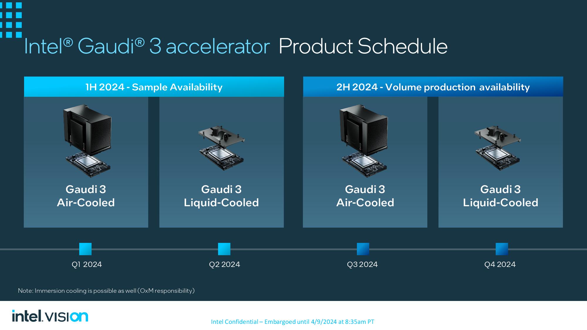
Dell, HPE, Lenovo, and Supermicro will provide systems for the Gaudi 3 launch. Gaudi air-cooled models have already been sampled, with sampling of liquid-cooled models to follow in Q2. These will be generally available (mass production) in Q3 and Q4 of 2024, respectively. The PCIe card will also be available in Q4.
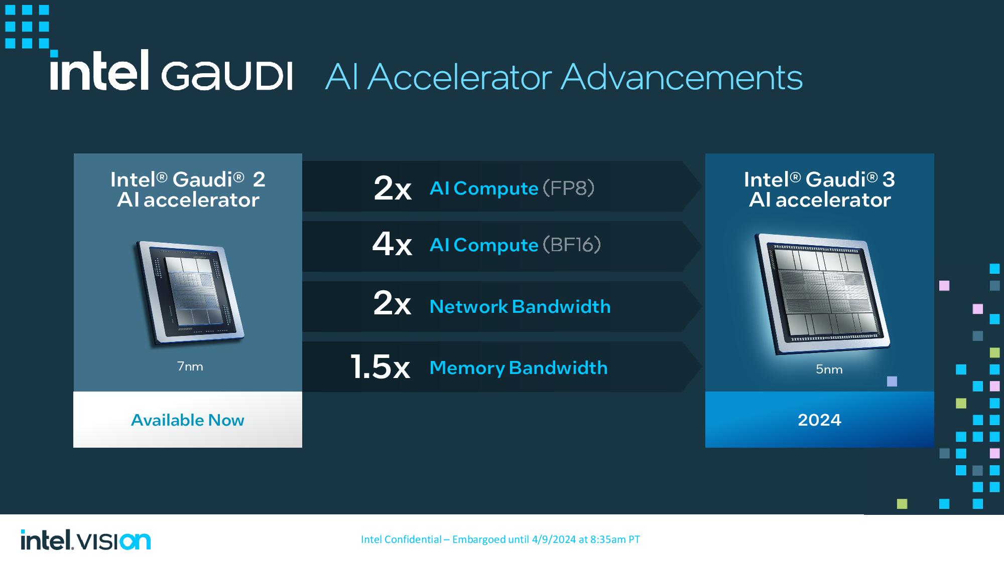
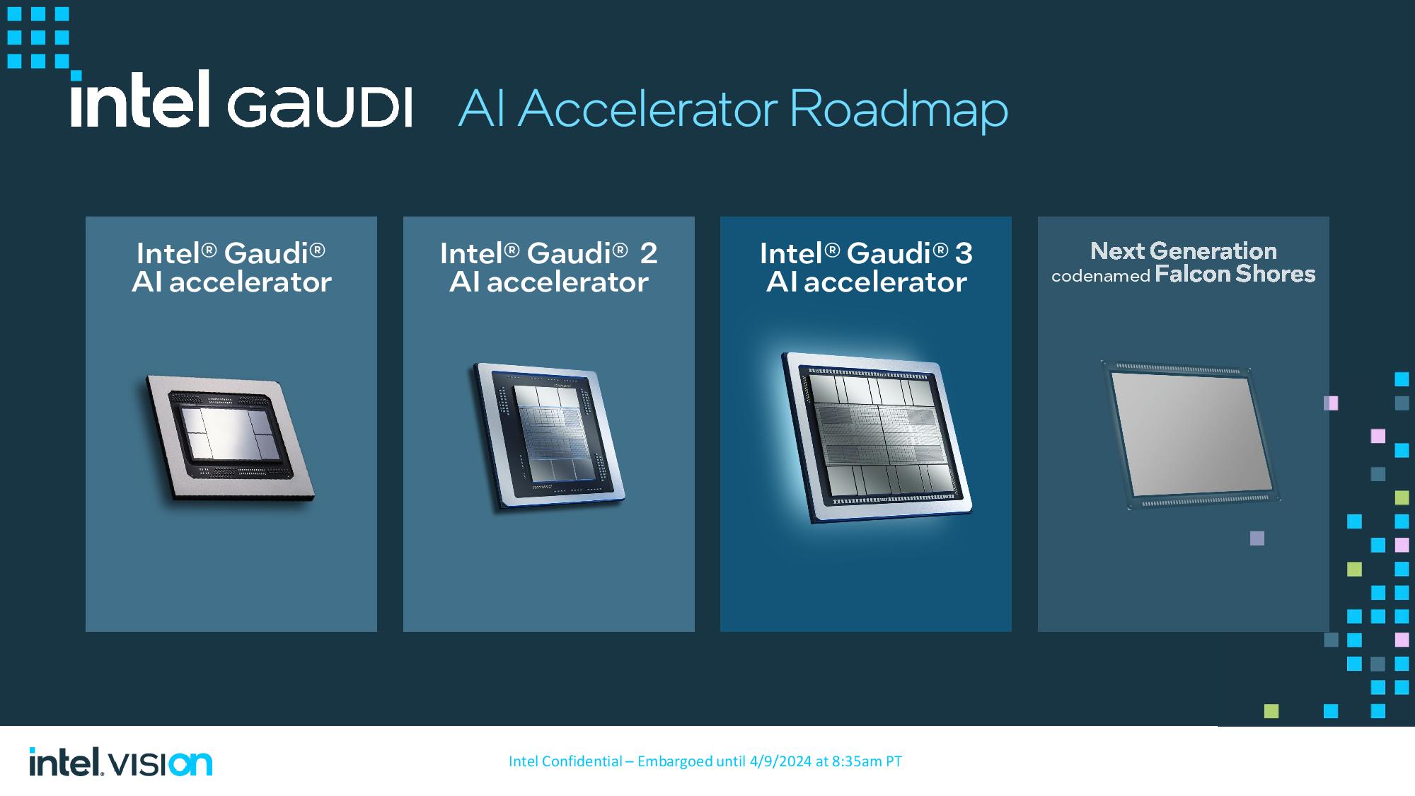
Gaudi 3 leverages the same architecture and underlying fundamental principles as its predecessor but comes with a more advanced TSMC 5nm process than the TSMC 7nm node Intel uses for the Gaudi 2 accelerator.
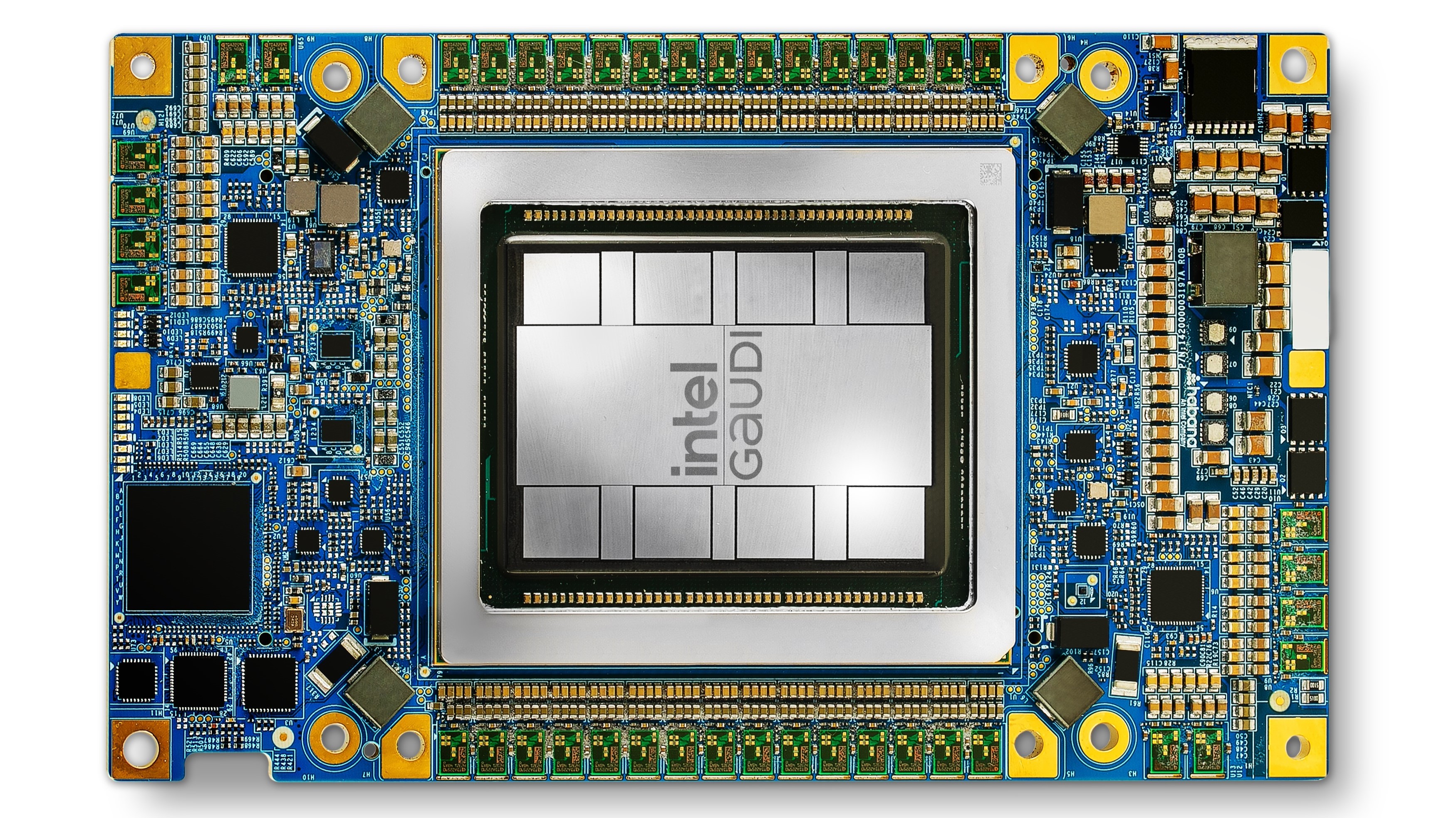
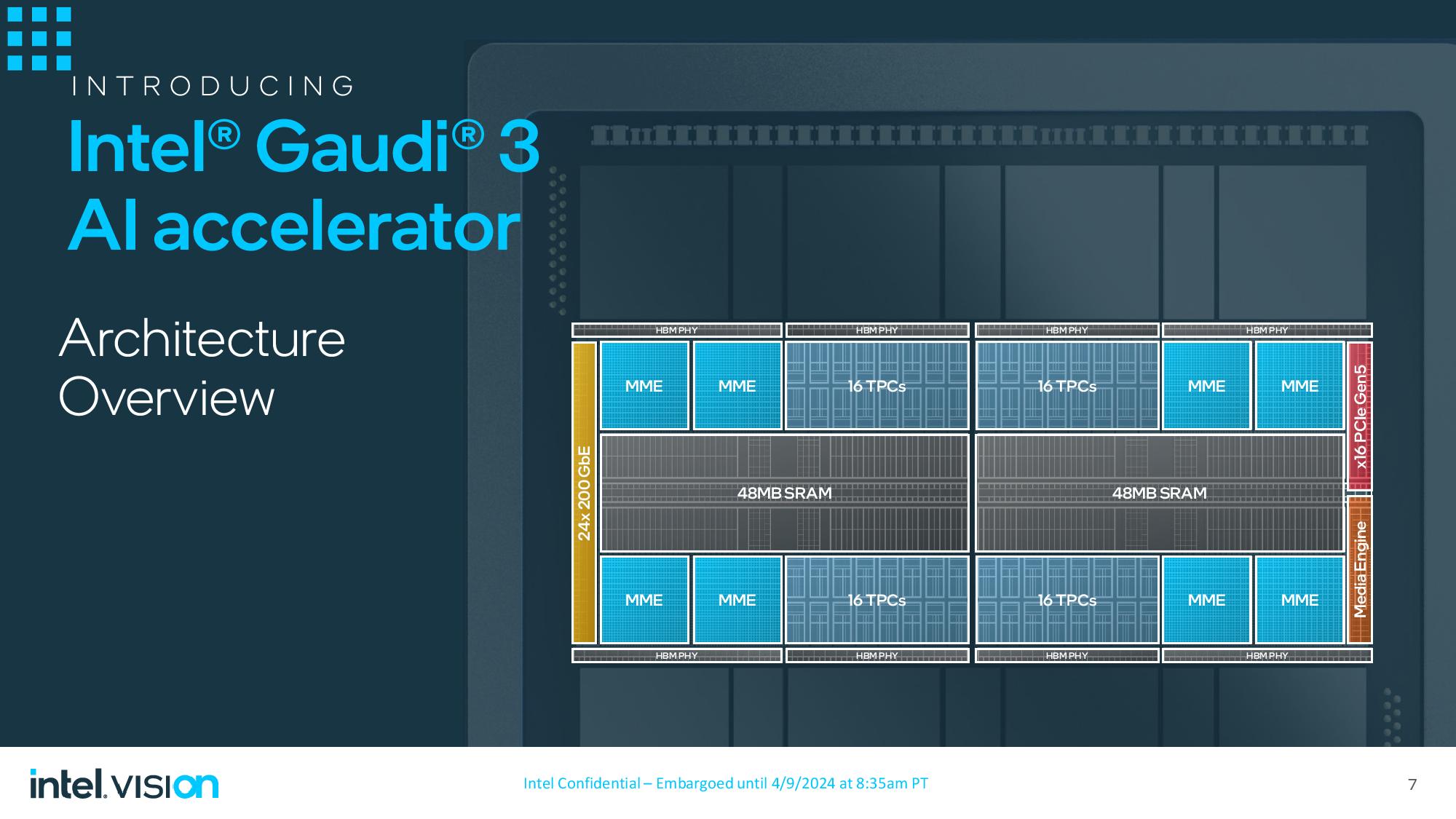
The OAM design has two central 5nm dies with 96MB of SRAM split between the two, providing 12.8 TB/s of bandwidth. The dies are flanked by eight HBM2E packages, totaling 128GB, that deliver up to 3.7 TB/s of bandwidth. A high-bandwidth interconnect between the two dies provides access to all memory present on both dies, thus allowing it to look and act as a single device (at least as far as the software is concerned - latency might vary). Gaudi 3 also has a x16 PCIe 5.0 controller for communication with the host processor (CPU) and different ratios of CPUs and Gaudi accelerators can be employed.
Compute is handled by 64 fifth-gen Tensor Processing Cores (TPC) and eight matrix math engines (MME), with workloads orchestrated between the two engines by a graph compiler and the software stack. The Gaudi 3 chip package also includes twenty-four 200 Gbps RoCE Ethernet controllers that provide both scale-up (in-box) and scale-out (node-to-node) connectivity, doubling the 100 Gbps connections on Gaudi 2.
Gaudi 3 Scalability
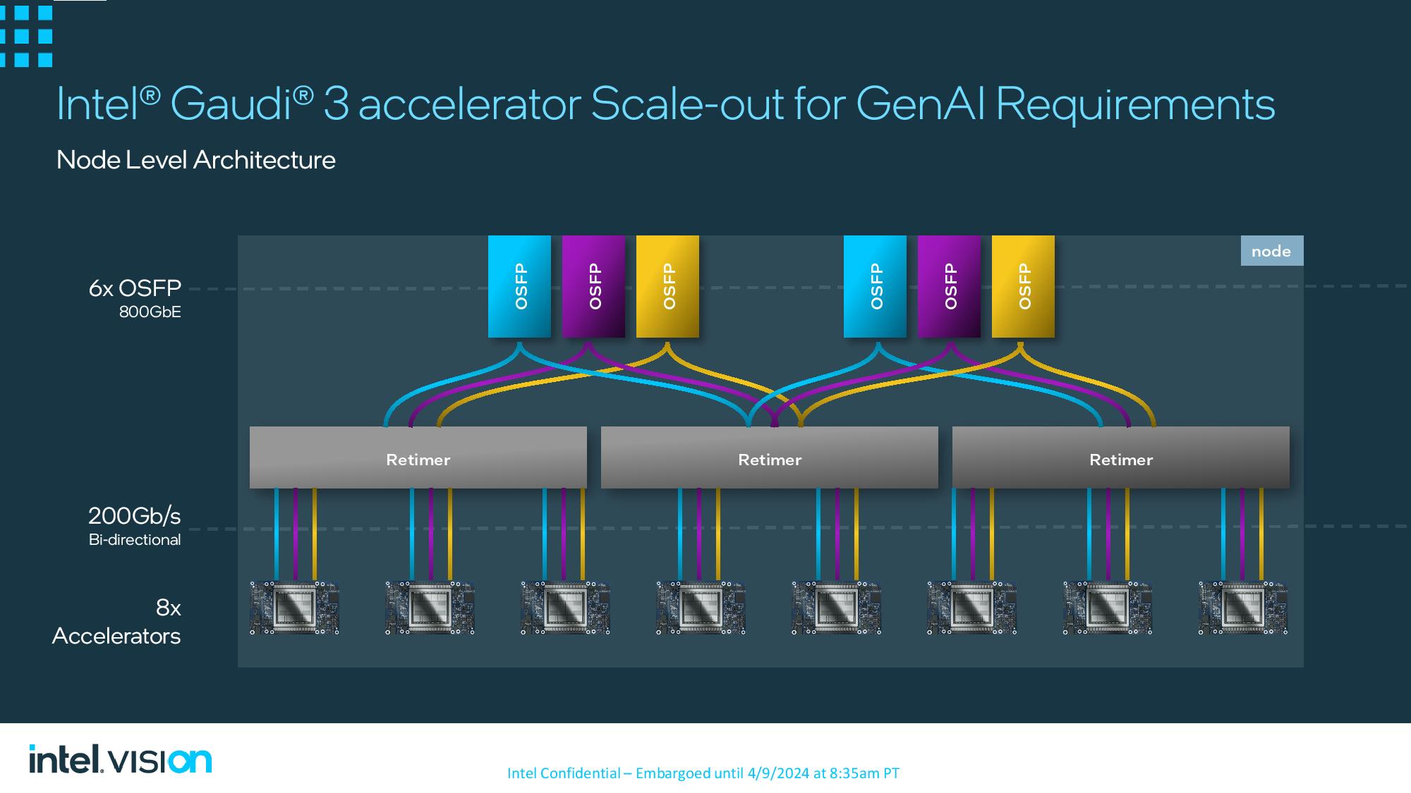
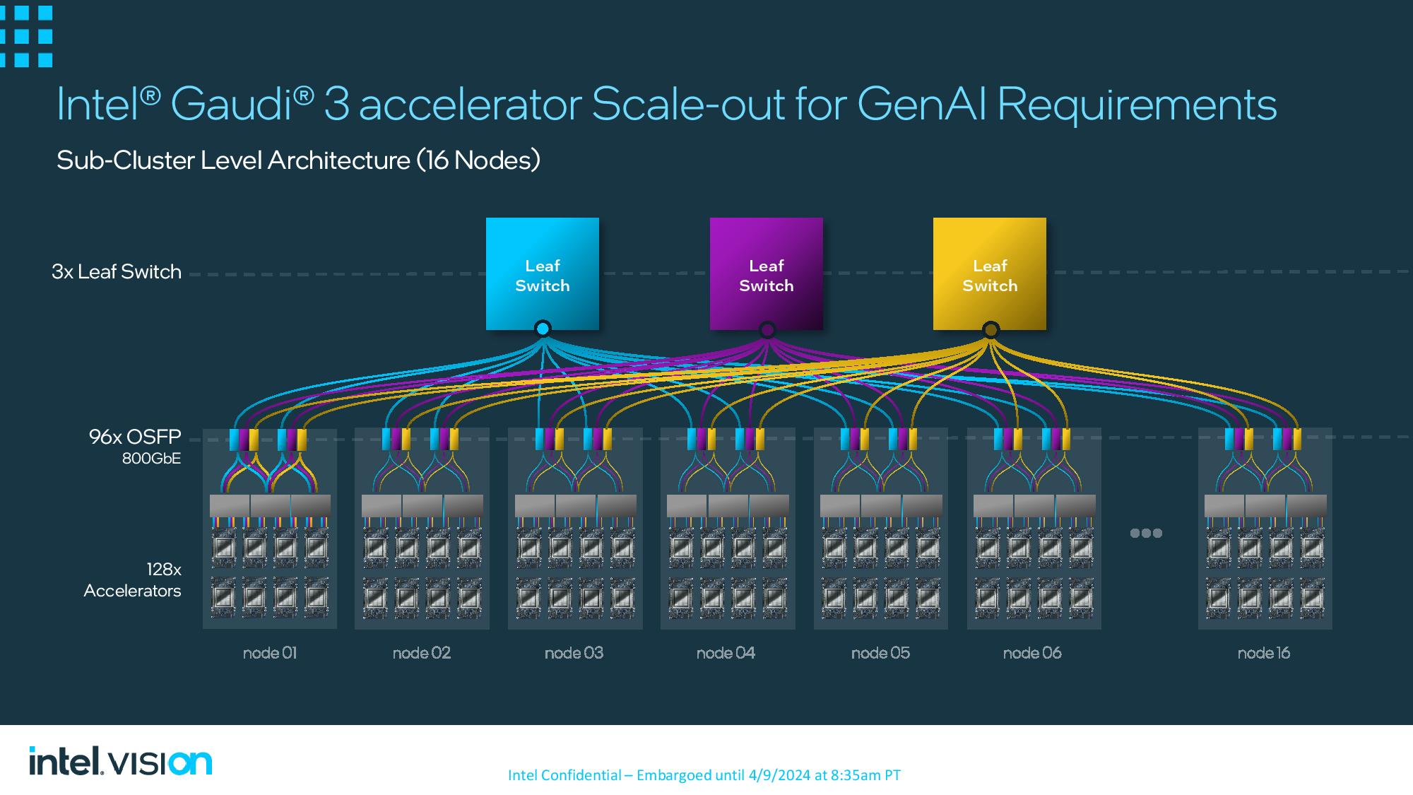
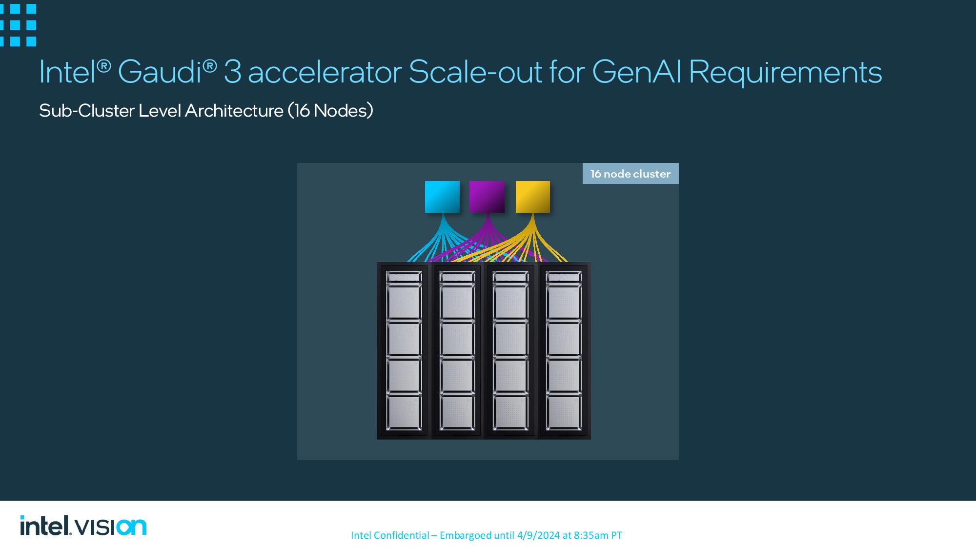
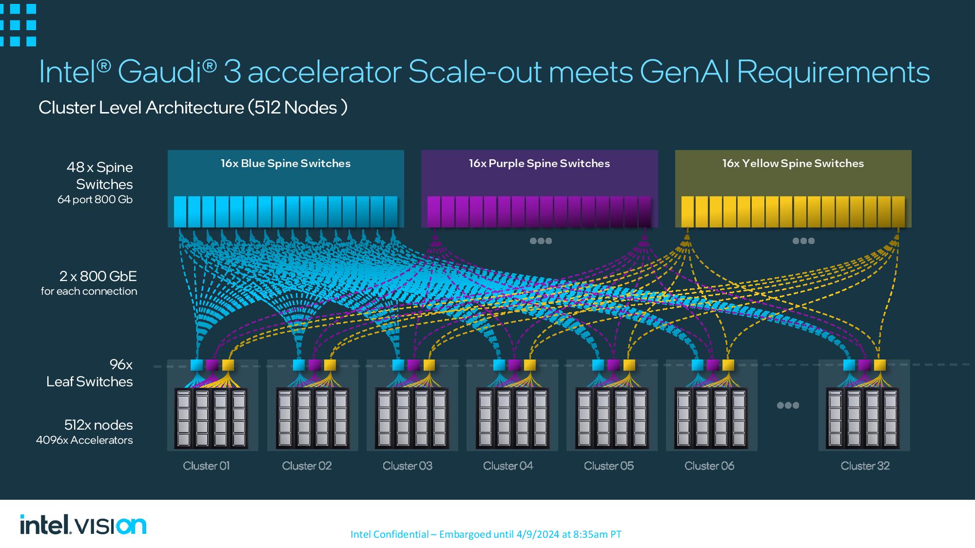
At the end of the day, the key to dominating today’s AI training and inference workloads resides in the ability to scale accelerators out into larger clusters. Intel’s Gaudi takes a different approach than Nvidia’s looming B200 NVL72 systems, using fast 200 Gbps Ethernet connections between the Gaudi 3 accelerators and pairing the servers with leaf and spine switches to create clusters.
Nvidia’s system-level architecture utilizes NVLink over the PCIe interface for both in-box connectivity between GPUs and stretching out to connect entire racks with passive copper cabling via its NVLink switches. AMD also has its own approach of using the PCIe interface and its Infinity Fabric protocol between GPUs residing in the server while using external NICs for communication with other nodes, but this adds more networking cost and complexity than Intel’s approach of having networking NICs built right into the chip.
Thanks to the doubled network bandwidth, Gaudi 3 scales from a single node with 8 OAM Gaudis to clusters with up to 1,024 nodes (servers) housing 8,192 OAM devices.
Each server is comprised of eight Gaudi 3 accelerators communicating with each other via twenty-one 200 Gbps Ethernet connections apiece. The remaining three Ethernet ports on each device are used for external communication with the cluster via a leaf switch. The switch aggregates these connections into six 800 Gbps Ethernet ports with OFSP connectors to facilitate communication with other nodes.
Each rack typically contains four nodes, but this can vary based on rack power limits and cluster size. Up to 16 nodes form a single sub-cluster with three Ethernet leaf switches, which then connect to spine switches, typically with 64 ports, to form even larger clusters. Half of the 64 ports on the 800 Gbps leaf switch are connected to the 16 nodes, while the remaining half connect to the spine switches.
Varying numbers of spine switches are used based on the size of the cluster, with Intel providing an example of three spine switches used for 32 sub-clusters comprised of 512 nodes (4,096 Gaudi’s). Intel says this configuration provides equal bandwidth for all server-to-server connections (non-blocking all-to-all). Adding another layer of Ethernet switches can support up to tens of thousands of accelerators.
Gaudi 3 performance vs Nvidia H100
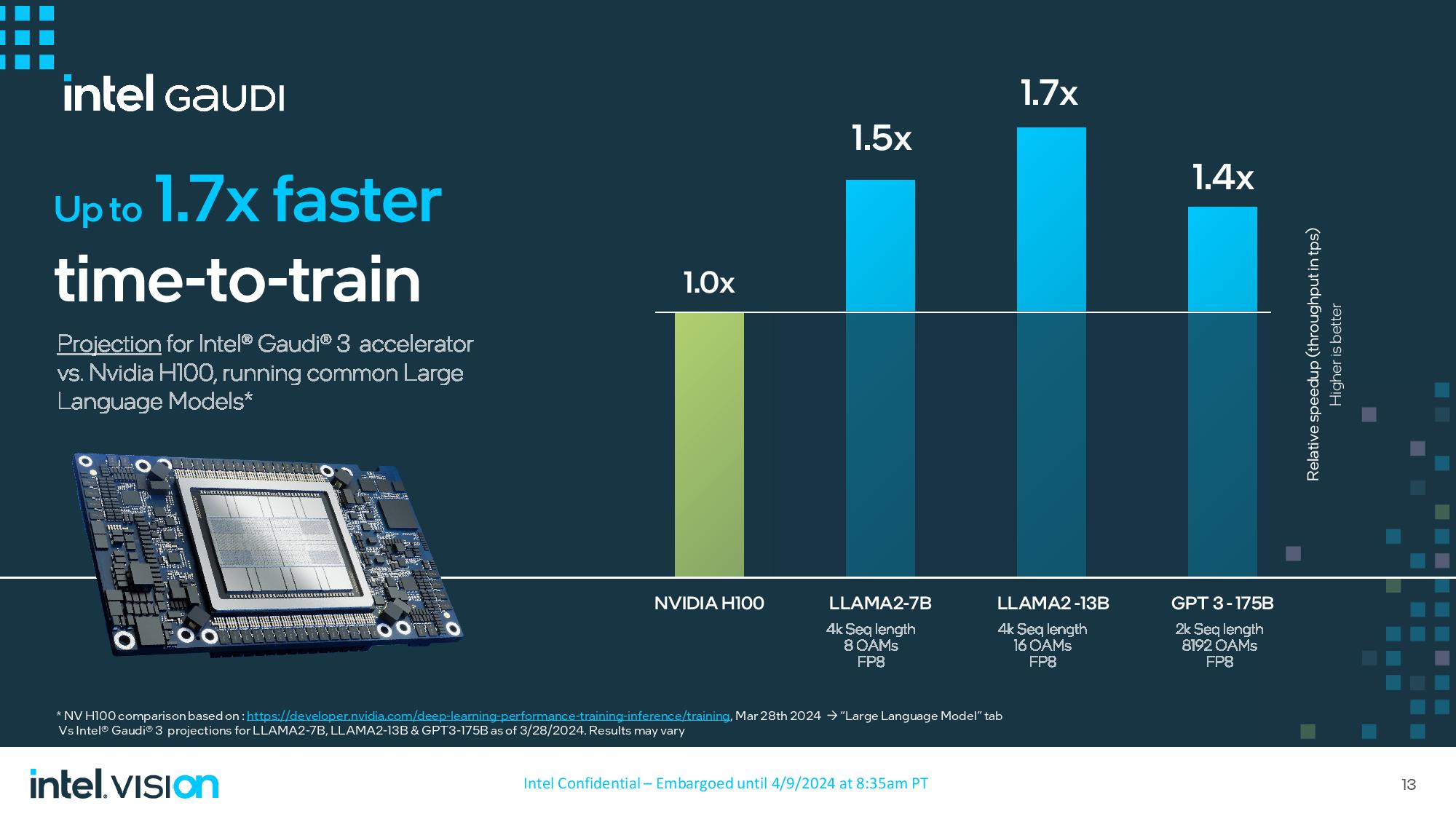
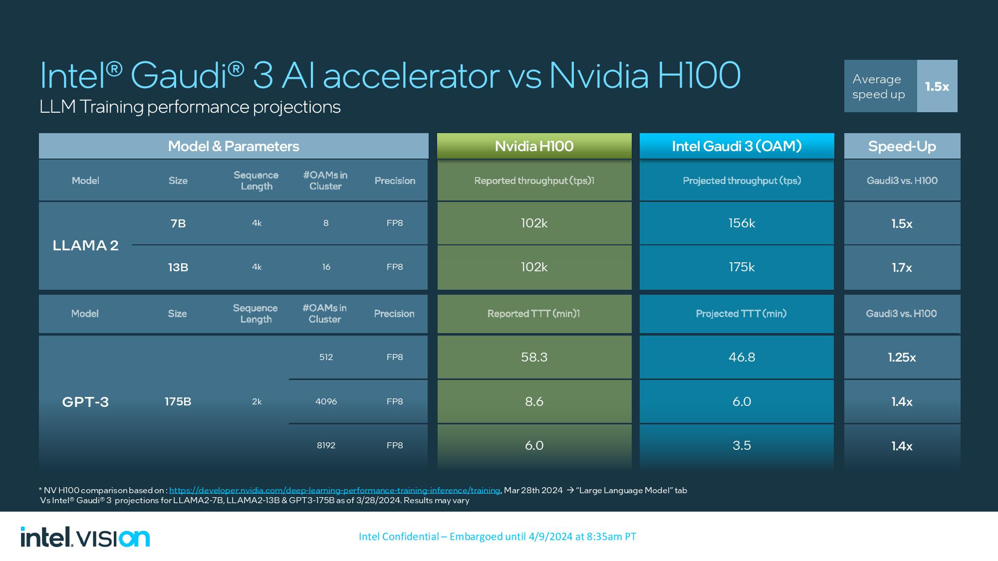
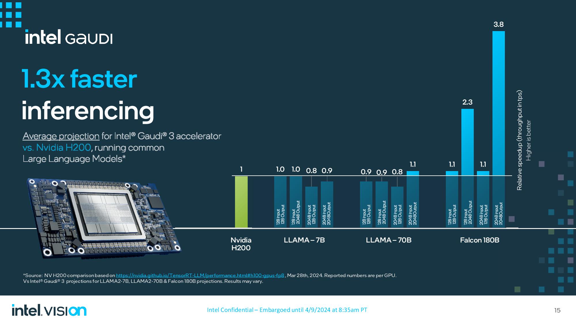
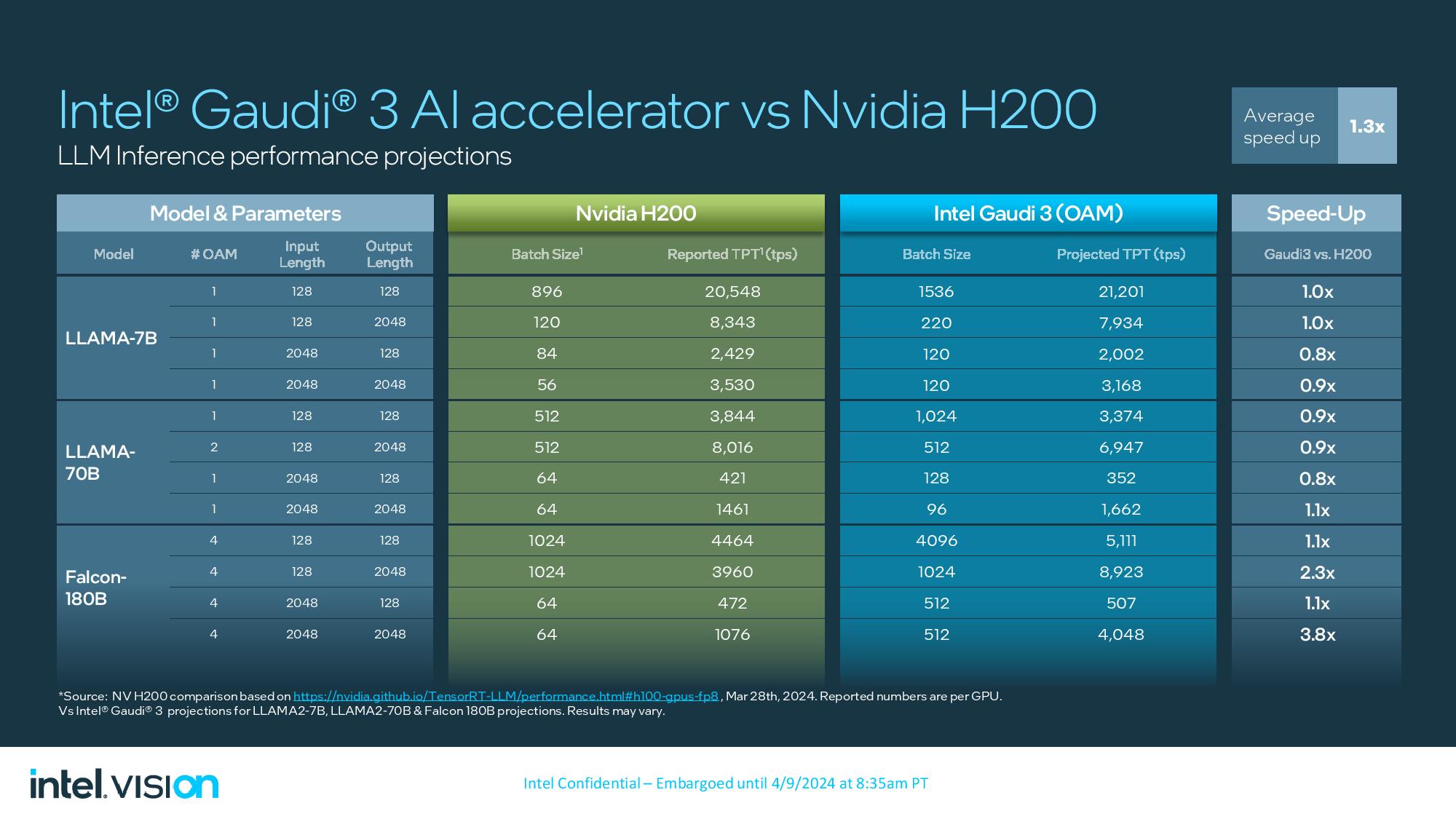
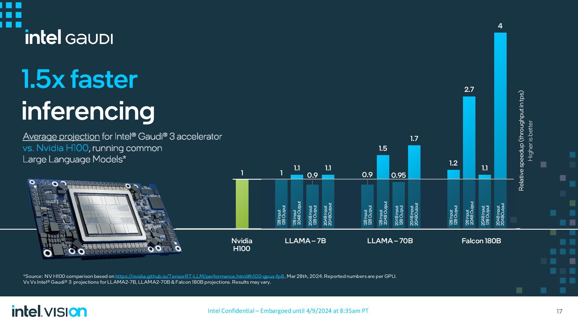
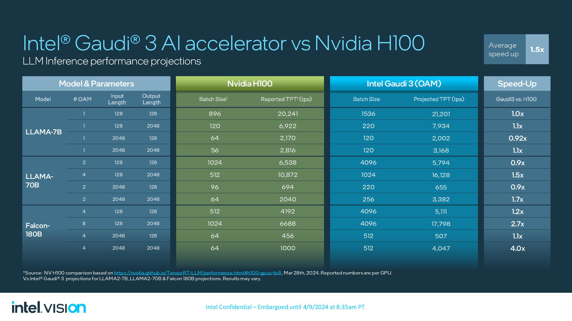
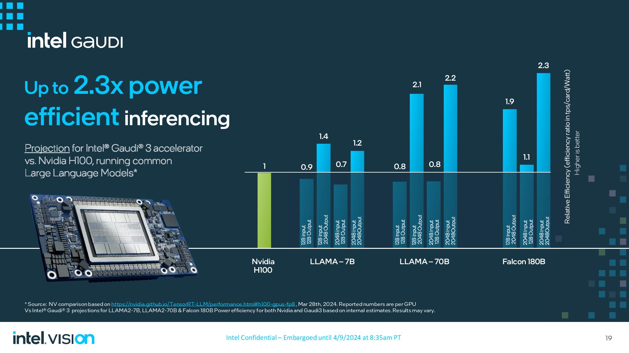
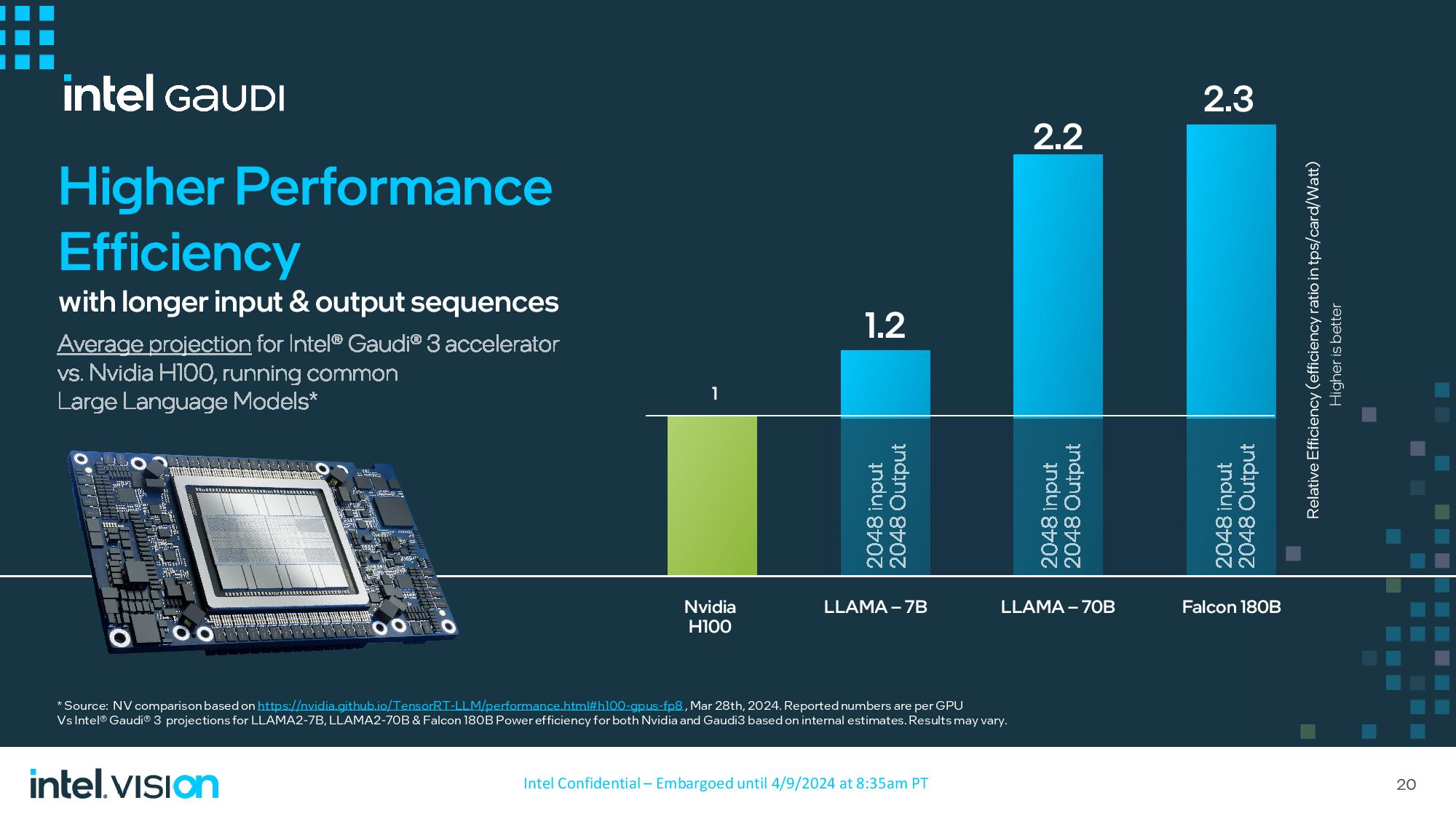

Intel shared performance projections for Gaudi 3, but as with all vendor-provided benchmarks, we should take these with a grain of salt. As you’ll see in the last image in the above album, Intel is now simply providing a QR code for information about its benchmarks instead of the line-by-line details of test configurations that it has provided in the past. This code doesn’t provide us with any meaningful way to look at the closer details of these test results and configurations, so add a shovelful of salt to any of these benchmark claims.
Intel compared to publicly available benchmarks for H100 systems but didn’t compare to Nvidia’s upcoming Blackwell B200 due to a lack of real-world comparative data. The company also didn’t provide comparisons to AMD’s promising Instinct MI300 GPUs, but that's impossible because AMD has continued to avoid publishing public performance data in the industry-accepted MLPerf benchmarks.
Intel provided plenty of comparisons in both training and inference workloads compared to the H100 with similar cluster sizes, but the key takeaway is that Intel claims Gaudi is from 1.5X to 1.7X faster in training workloads. Comparisons include LLAMA2-7B (7 billion parameters) and LLAMA2-13B models with 8 and 16 Gaudi’s, respectively, and a GPT 3-175B model tested with 8,192 Gaudi accelerators, all using FP8. Interestingly, Intel didn’t compare to Nvidia’s H200 here, which has 76% more memory capacity and 43% more memory bandwidth than the H100.
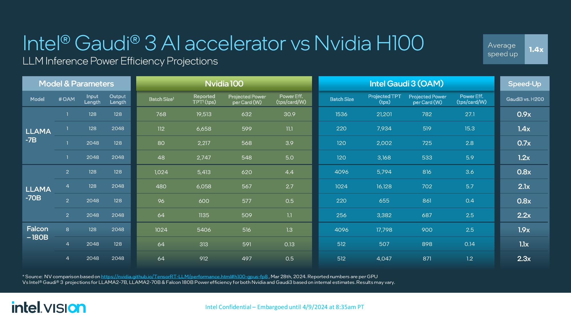
Intel did compare to the H200 for its inference comparisons but stuck to performance with a single card as opposed to comparing scale-out performance with clusters. Here we can see a mixed bag, with five of the LLAMA2-7B/70B workloads coming in 10 to 20% below the H100 GPUs, while two match and one slightly exceeds the H200. Intel claims Gaudi's performance scales better with larger output sequences, with Gaudi delivering up to 3.8 times the performance with the Falcon 180 billion parameter model with a 2,048-length output.
Intel also claims up to a 2.6X advantage in power consumption for inference workloads, a critical consideration considering restrictive power limits in data centers, but it didn’t provide similar benchmarks for training workloads. For these workloads, Intel tested a single H100 in a public instance and logged the H100’s power consumption (as reported by the H100) but didn’t provide examples of inference with a single node or larger clusters. With larger output sequences, Intel again claims better performance and, thus, efficiency.
Gaudi 3 software ecosystem
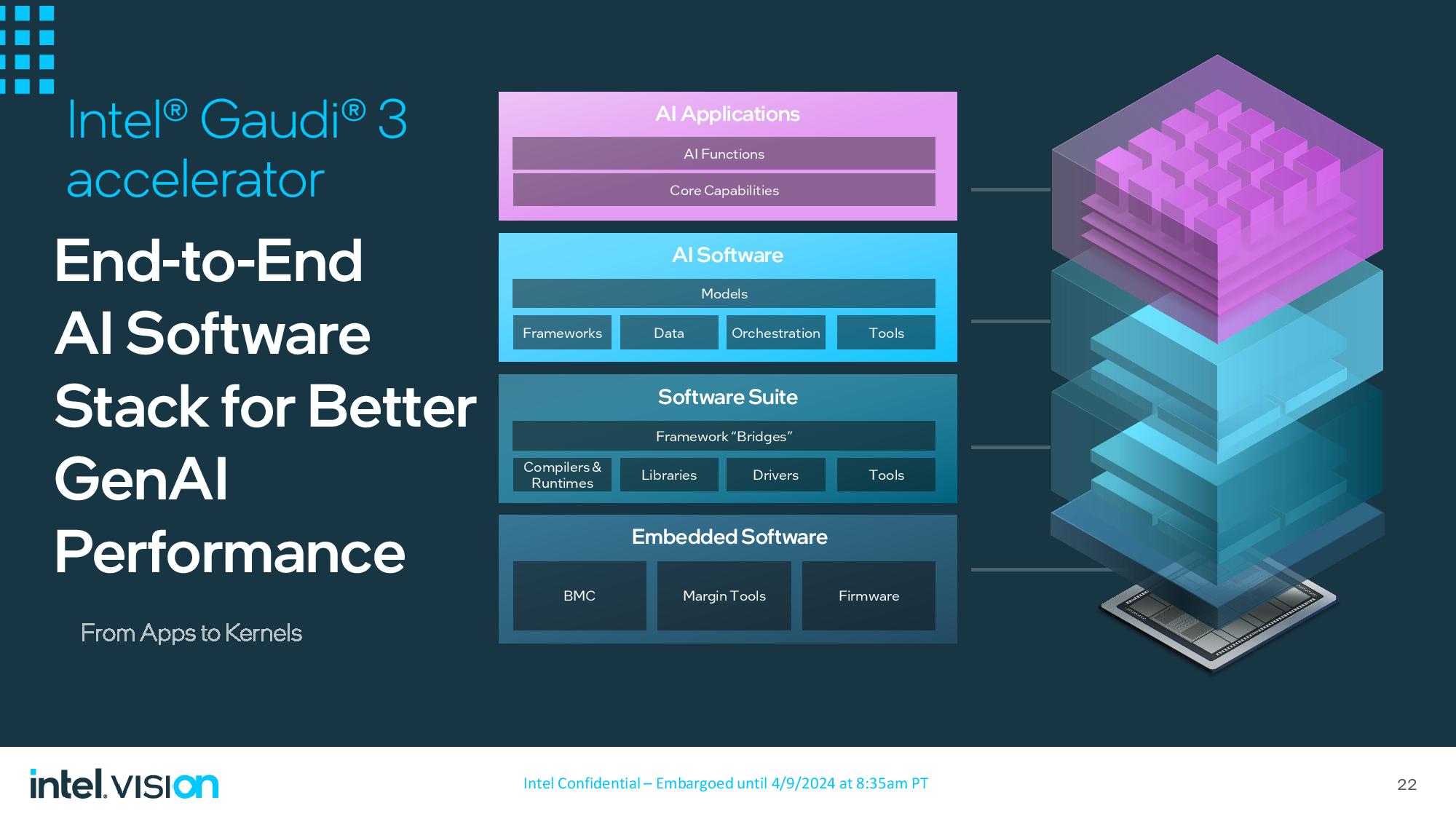
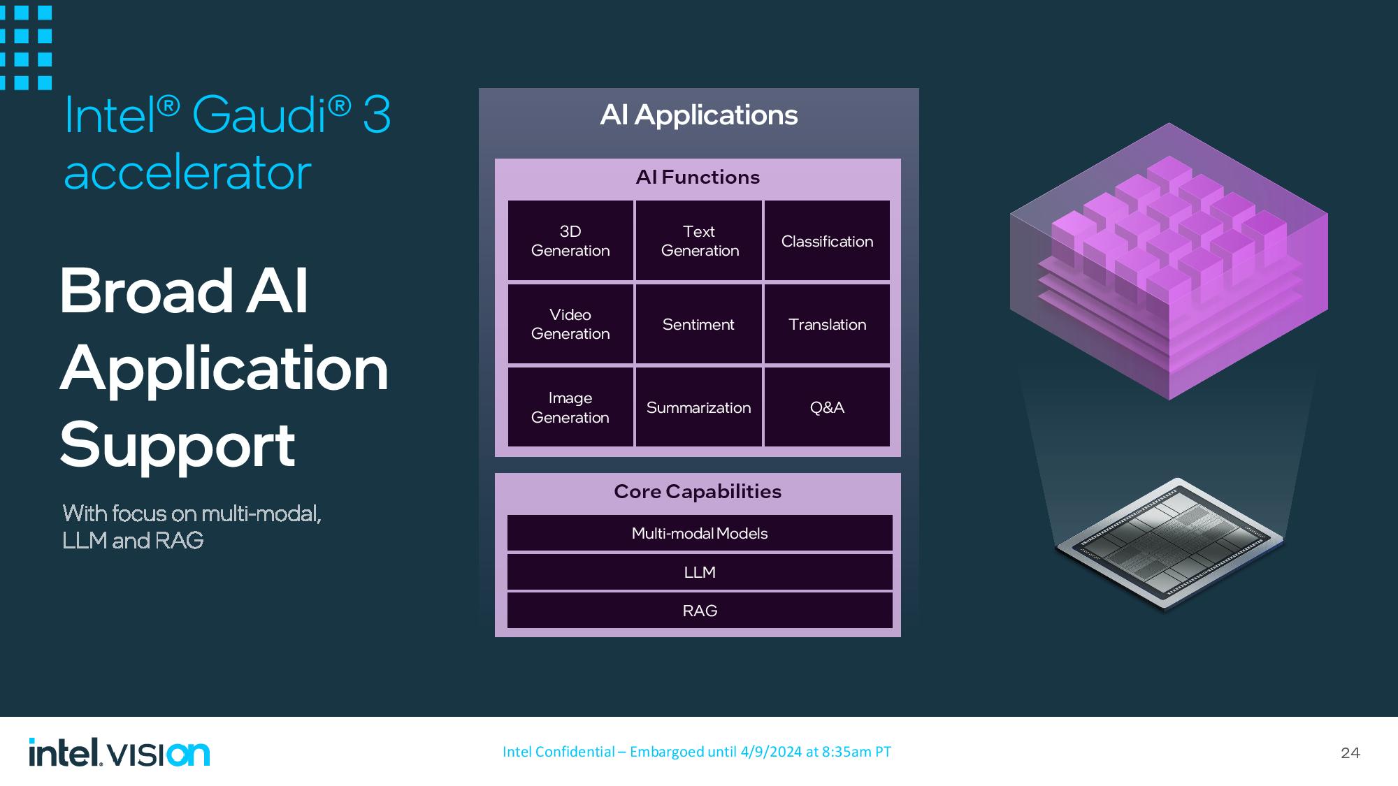
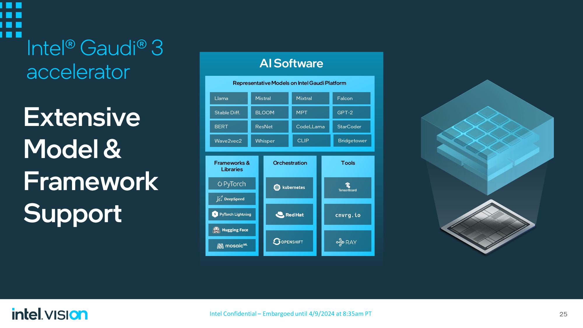
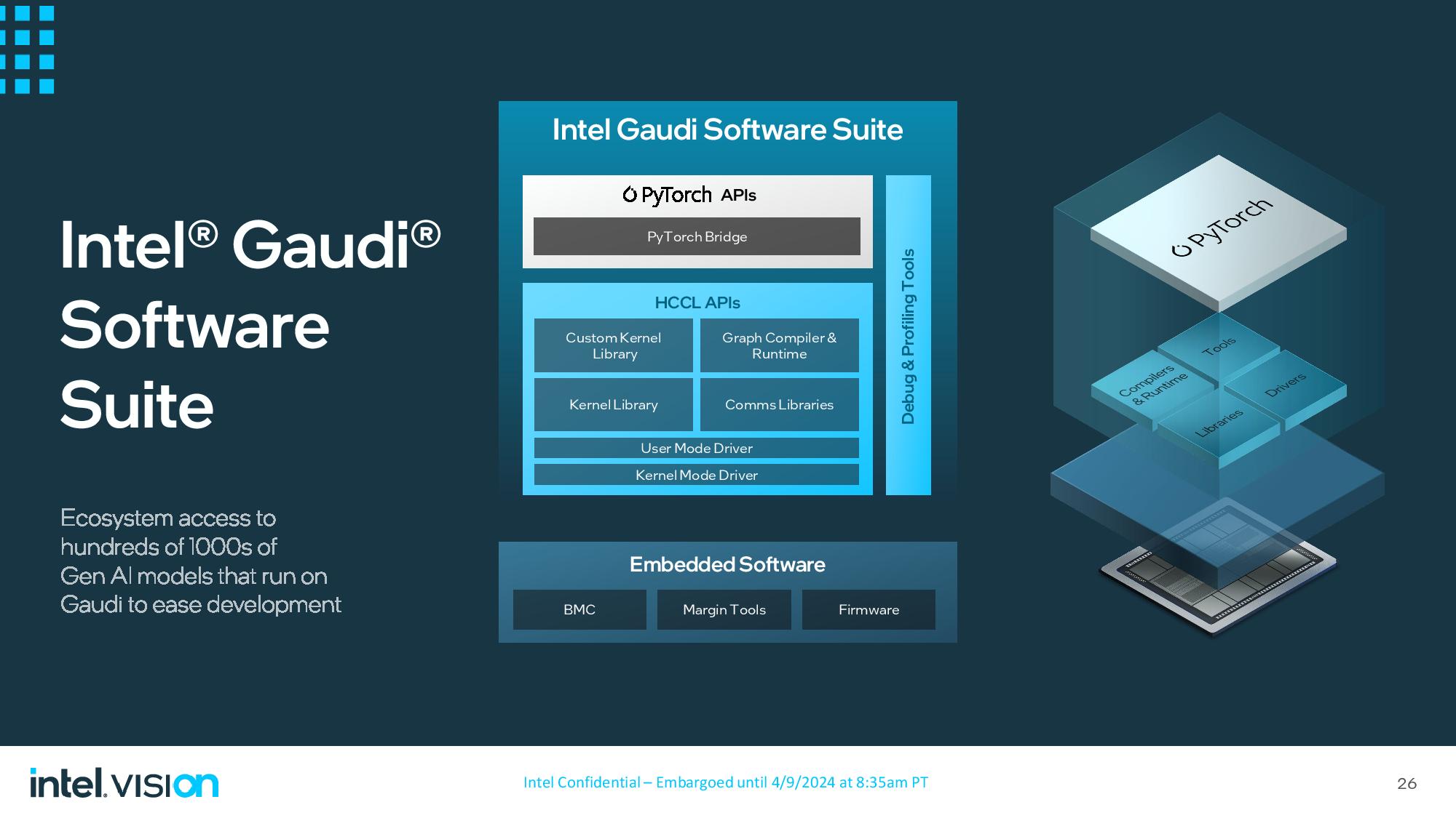
As Nvidia’s dominance with CUDA has illustrated, the software ecosystem is just as critical of a consideration as the hardware. Intel touts its end-to-end software stack and says that “most” of its engineers are currently working on bolstering support. Intel’s current focus is on supporting multi-modal training and inference models and RAG (retrieval augmented generation).
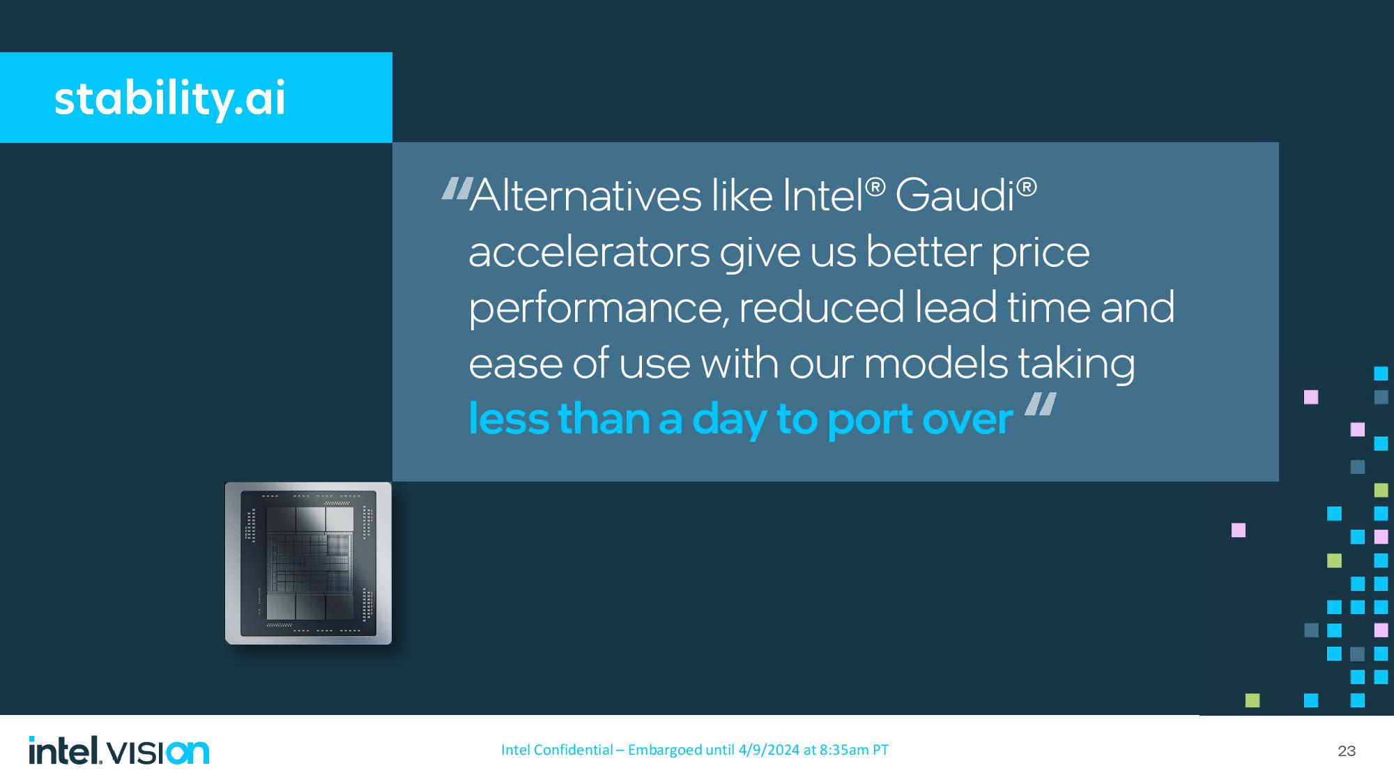
Hugging Face has over 600,000 AI model checkpoints available, and Intel says its work with Hugging Face, PyTorch, DeepSpeed, and Mosaic has eased the software porting process to enable faster turnaround times for deploying Gaudi 3 systems. Intel says most programmers are programming at the framework level or above (i.e., simply using PyTorch and scripting with Python) and that low-level programming with CUDA isn’t as common as perceived.
Intel’s tools are designed to ease the porting process while abstracting away the underlying complexity, with OneAPI serving as the underlying kernel and communication libraries. These libraries adhere to the specifications outlined by the Unified Accelerator Foundation (UXL), and industry consortium that includes Arm, Intel, Qualcomm, and Samsung, among others, that's intended to provide an alternative to CUDA. PyTorch 2.0 is optimized for using OneAPI for inference and training with Intel CPUs and GPUs. Intel says its OpenVino also continues to enjoy rapid adoption, with over one million downloads so far this year.
Thoughts
As we covered above, Intel, Nvidia, and AMD are all taking different paths to providing the enhanced cluster scalability that is key to performance in both AI training and inference workloads. Each approach has its own respective strengths, but Nvidia's proprietary NVLink is the most mature and well-established solution, and its extension to rack-scale architectures is a significant advantage. That said, Intel's approach with Ethernet-based networking brings an open solution that affords plenty of customization options by supporting networking switches from multiple vendors, and its built-in NICs also offer cost advantages over AMD's competing Instinct MI300 series.
However, both Nvidia's Grace-based products and AMD's MI300A offer sophisticated merged CPU+GPU packages that will be hard to beat in some workloads, while Intel continues to rely on separate CPU and accelerator components due to its cancellation of the merged CPU+GPU version of Falcon Shores. There have been reports of Nvidia's new GB200 CPU+GPU servers comprising the bulk of the company's Blackwell orders, highlighting the industry's voracious appetite for these types of tightly-coupled products.
Intel's future Falcon Shores product will arrive as an AI accelerator-only design, so it will still be able to compete with GPU-only Nvidia and AMD clusters. We also see room for a refresh generation of Gaudi 3 that moves from HBM2E to HBM3/E—both AMD and Nvidia employ the faster memory in their AI products. Although it hasn't shared hard data, Intel says it also plans to compete aggressively on pricing, which might be a powerful recipe as Nvidia continues to grapple with shortages due to crushing demand for its GPUs.
Falcon Shores will also be compatible with code optimized for Gaudi, providing forward compatibility. Intel also cites a 3X improvement to its Gaudi 2 platform over the last several quarters as an example of increased adoption of its platform.
Notably, Intel didn't promote its Ponte Vecchio GPUs for the event, which isn't surprising given its cancellation of the next-gen Rialto Bridge GPUs, so we expect the company's AI efforts to coalesce solely on Gaudi 3 as it prepares Falcon Shores for launch next year.
The air-cooled Gaudi 3 models are already sampling to partners, with general availability in Q3. Liquid-cooled models will follow in Q4. We're watching the Intel Vision webcast for further details and will update as neccesary.

Paul Alcorn is the Editor-in-Chief for Tom's Hardware US. He also writes news and reviews on CPUs, storage, and enterprise hardware.
-
thisisaname So energy efficient may if the world used these instead of Nvidia the energy problems with AI would end over night! /sReply -
CmdrShepard They can say it's faster and cheaper than NVIDIA, but in the end TCO depends on power usage / efficiency and also on the amount of money you need to spend writing and maintaining custom software for their card.Reply
That's why people will continue buying NVIDIA. -
gg83 Reply
The software and ecosystem are key to AI Accelerator adoption right?sjkpublic said:Intel using 200GBps network interface vs everyone using PCIe? Another bad decision? I am not seeing any real world stats. And it is unclear how the software platforms in use will drive Intel forward or reverse. Intel has been in reverse for a long time. -
JayNor "Intel also announced that it is developing an AI NIC ASIC for Ultra Ethernet Consortium-compliant networking and an AI NIC chiplet that will be used in its future XPU and Gaudi 3 processors..."Reply
Gaudi 3 processors are already sampling. So are their NIC chiplets UEC-compliant? -
JayNor Reply
Intel also put PCIE5 X16 on each of the 8 Gaudi3 modules. In the Supermicro Gaudi3 server, there are 8 Gaudi3 modules, and the host CPU is reportedly a Granite Rapids-AP, with 136 PCIE5 lanes.sjkpublic said:But Intel has a habit of muddying the waters. They took there CPU and designed cores that have different power properties which IMHO was insane and added unnecessary complexity. So now lets makes fast ethernet connections a 'thing' when in fact we can use the PCIe bus which is MUCH faster.
So, there is PCIE5 if you prefer that.
I think the Gaudi focus is on using their per NIC RoCE v2 DMA controllers, and controlling data transfers in a fully distributed manner. That's a lot of DMA going on without having to rely on a CPU. -
JayNor not clear why you consider pcie5 (32GT/sec) "PCIe bus which is MUCH faster"Reply
The Gaudi 3 ethernet signals are being routed around as
48 x 112Gb/s PAM4 SerDes Links
let's see the math
https://www.intel.com/content/www/us/en/content-details/817486/intel-gaudi-3-ai-accelerator-white-paper.html -
sjkpublic Reply
Thank you for correcting me. My fault. I have deleted my posts as they are misinformation.JayNor said:not clear why you consider pcie5 (32GT/sec) "PCIe bus which is MUCH faster"
The Gaudi 3 ethernet signals are being routed around as
48 x 112Gb/s PAM4 SerDes Links
let's see the math
https://www.intel.com/content/www/us/en/content-details/817486/intel-gaudi-3-ai-accelerator-white-paper.html