









Micron unveils DDR5-9200 memory: 1γ process technology with EUV
Micron finally adopts EUV for DRAM.
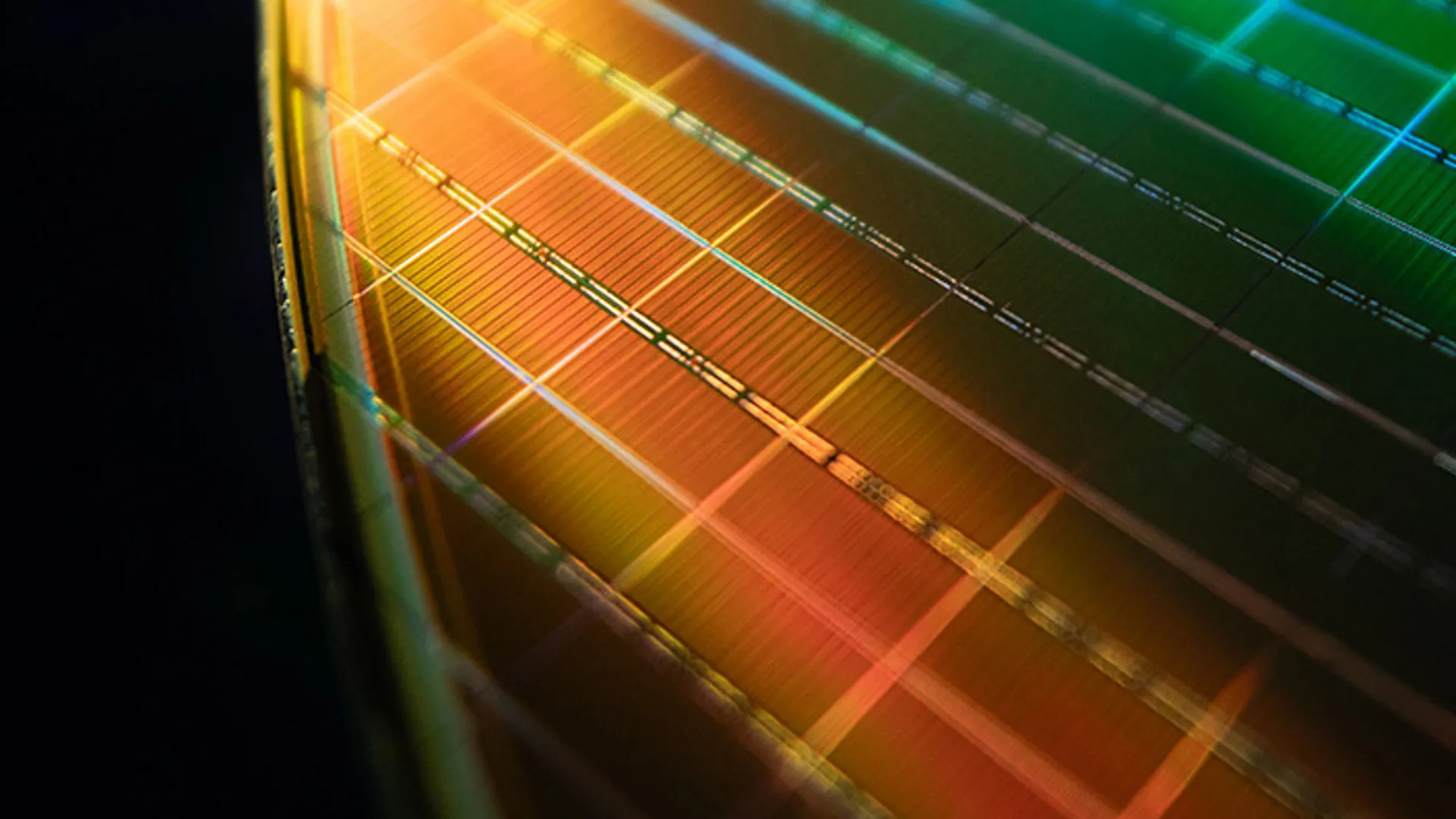
Micron introduced its 16Gb DDR5 devices made on its new 1γ (1-gamma) fabrication process that uses EUV lithography, a first for Micron, today on March 25. The new IC not only delivers higher performance than its predecessor, but it also consumes less power and is poised to be cheaper to make. The company also said that its 1γ manufacturing technology (6th Generation 10nm-class node) will eventually be adopted for other DRAM products.
DDR5 at 9200 MT/s
Micron's lead 1γ product is the company's 16Gb (2GB) DDR5 IC that is rated for a 9200 MT/s data transfer rate at an industry-standard voltage of 1.1V. Compared to its predecessor — a 16Gb DDR5 IC made on 1β fabrication process — the new device consumes 20% less power and features a 30% higher bit density, which may translate into a comparable decrease in production cost once the new chips achieve yields comparable to that of 1β 16Gb DRAM devices.

While Micron rates its latest 16Gb DDR5 ICs at 9200 MT/s, this speed bin is significantly higher than anything in the latest edition of the DDR5 specification. The company stresses that the chip can run at JEDEC-compliant speed grades just fine, and the higher speed bin will enable some future proofing and compatibility with next-generation CPUs. Micron also suggests that CUDIMMs or CXL-based memory modules could leverage higher-than-JEDEC speeds. DIMMs for enthusiasts will also likely adopt the new DRAMs for their post-10,000 MT/s modules.
Micron is currently sampling its 16Gb DDR5 ICs made on 1γ technology and products on their base (i.e., chips and modules) with laptop and server manufacturers and expects their qualifications to be completed in one or two quarters. That means we should see Micron's latest memory devices in retail products starting mid-2025. The company expects all types of memory modules — for desktops, laptops, and servers — to adopt its new memory chips.
Considering the fact that Micron's 1γ-based DRAMs offer a combination of valuable qualities for all market segments — enhanced performance for desktops as well as lower power consumption for notebooks and servers — we indeed expect the firm's latest 16 Gb DDR5 ICs to become quite popular when they hit the market.

Over time, Micron will use its 1γ fabrication technology to make other types of memory products, including GDDR7, LPDDR5X (at up to 9600 MT/s), and data center-grade products, so the node will become a workhorse for the company.
1γ manufacturing technology
Micron's 1γ manufacturing process is the company's first technology to adopt extreme ultraviolet lithography (EUV), something that other leading memory makers adopted years ago. It's been a while in coming and looks to offer significant benefits relative to existing product lines.

Micron did not disclose how many EUV layers the new production node uses, but we can speculate that the company uses EUV for critical layers that would otherwise require the usage of multi-patterning, which lengthens production cycles and can affect yields. Micron does say that 1γ uses EUV in conjunction with multi-patterning DUV techniques. Also, Micron's 1γ DRAM process technology adopts next-generation high-K metal gate technology and an all-new back-end-of-line (BEOL) circuitry.
" In addition to EUV adoption in 1γ, we have introduced our next generation high-K metal gate CMOS and advanced back-end-of-line processes, which together enable the 9200 MT/s [data transfer rate], a 15% performance improvement over 1β DRAM […] while reducing power by about 20% over 1β," said Shigeru Shiratake, senior vice president of DRAM Technology Development at Micron.
For now, Micron produces its 1γ DRAMs at its fabs in Japan, where the company's first EUV tool was installed in 2024. As the company ramps up production of 1γ memory, it will add more EUV systems to its fabs in Japan and Taiwan.
Get Tom's Hardware's best news and in-depth reviews, straight to your inbox.

Anton Shilov is a contributing writer at Tom’s Hardware. Over the past couple of decades, he has covered everything from CPUs and GPUs to supercomputers and from modern process technologies and latest fab tools to high-tech industry trends.
-
Notton I find it interesting they are boasting about the EUV process with slides, rather than the high-k material that made the capacitor size shrink possible.Reply
Is 1γ a 8nm to 10nm node size? -
Jame5 ReplyAaron Priest said:RAM so fast it time traveled! I think you meant today on February 25. ;-)
Exactly that!
Anton Wrote:
Micron, today on March 25. -
DS426 Reply
Article says 1γ is Micron's 6th-gen 10nm class node.Notton said:...
Is 1γ a 8nm to 10nm node size? -
thestryker I wonder if this will mean Micron DDR5 IC will be viable for high performance kits finally. I don't think I'd move back to lower capacity modules, but it would be nice if SK Hynix had some actual competition. In theory that might knock down the prices on the higher performance kits.Reply
Yeah it's in that general area. Due to the trouble with shrinking memory all of the manufacturers have obfuscated their process for years now. I think SK Hynix was the first of the three to use EUV which may explain their dominance in the DDR5 era.Notton said:Is 1γ a 8nm to 10nm node size? -
MegaZeroX First of all, I'm typing this from a cell phone so sorry for any sloppiness.Reply
Typo in the main article: I assume "March 25th" is meant to be "February 25th"
Notton said:I find it interesting they are boasting about the EUV process with slides, rather than the high-k material that made the capacitor size shrink possible.
Is 1γ a 8nm to 10nm node size?
For context, cell sizes are measured with 6F^2. IIRC, the previous feature size (F) for 1-beta was slightly over 13nm (as in, something like 13.1nm) which put it behind Samsung and SK Hynix which were slightly below 13nm (something like 12.9nm). Tokyo Electron's generic roadmap for investors put "12-11nm" as the feature size of 1-c/1-gamma, so it's likely in that range. -
usertests I hate those marketing names.Reply
>30% density sounds like you can go from 24 Gb to 32 Gb, so do that please. -
MegaZeroX I went back to check, and the F for 1b/1β was 12.54nm for Samsung, 12.65nm for SK Hynix, and 13.04nm for Micron. This data is from Tech Insights using a TEM.Reply