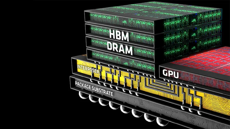
HBM4 memory is expected to drastically increase peak memory bandwidth thanks to its 2048-bit interface, which will be very useful for bandwidth-hungry artificial intelligence (AI) and high-performance computing (HPC) processors. But HBM4 will require a lot of changes to how high-bandwidth memory is made and integrated, which requires an even closer collaboration between logic foundries and memory makers. TSMC and SK Hynix certainly know that, which is why they reportedly formed an alliance to co-produce HBM4.
Maeil Business News Korea reports that TSMC and SK Hynix have formed the so-called AI Semiconductor Alliance that will combine the strengths of both companies in their respective field and align their strategies under the 'one-team strategy' principle. The report says that TSMC will handle 'some of HBM4' processes, which most likely means producing HBM4 base dies using one of its advanced process technologies that SK Hynix does not have. This corroborates with an earlier report claiming that HBM4 will require base dies made on a 12nm-class production node. Another report claims that SK Hynix and Nvidia are working on a technology that would stack HBM memory directly on top of processors without a substrate.
| null | HBM4 | HBM3E | HBM3 | HBM2E |
| Interface Width | 2048-bit | 1024-bit | 1024-bit | 1024-bit |
| Max Capacity Stack (up to) | 36 GB - 64 GB | 36 GB | 24 GB | 16 GB |
| Data Transfer Rate | ? | 9.2 GT/s | 6.4 GT/s | 3.6 GT/s |
| DRAM ICs per Stack | 16 | null | null | 8 |
| Bandwidth per Stack (up to) | 1.5 TB/s - 2+ TB/s | 1.2 TB/s | 819.2 GB/s | 460.8 GB/s |
Bot collaboration over HBM4 base dies is not the only aspect of TSMC's and SK Hynix's joint work. As part of its 3DFabric Memory Alliance, TSMC is working with all three makers of HBM, including Micron, Samsung, and SK Hynix. When it comes to SK Hynix, the companies are collaborating on CoWoS packaging for HBM3 and HBM4, Design Technology Co-Optimization (DTCO) for HBM, and even UCIe for HBM physical interface, according to a TSMC presentation demonstrated last year.
One of the reasons for the collaboration between TSMC and SK Hynix is that they need to work very closely to ensure that HBM3E and HBM4 memory from SK Hynix works with chips made by TSMC. After all, SK Hynix leads the HBM market, whereas TSMC is the world's largest foundry.
Meanwhile, Maeil Business News Korea also notes that the collaboration between TSMC and SK Hynix is meant to 'to establish a united front against Samsung Electronics,' which competes against both companies as it makes logic and memory chips. Reports like this are not uncommon and should be taken with a grain of salt. It is hard to imagine that TSMC would intentionally limit the compatibility of its packaging technologies to SK Hynix's memory, so it is likely that TSMC and SK Hynix are simply working a little deeper together than TSMC does with Samsung.
