SK Hynix and Nvidia reportedly working on a radical GPU redesign that 3D-stacks HBM memory directly on top of the processing cores
SK Hynix is working with Nvidia, other logic designers on HBM4 integration.

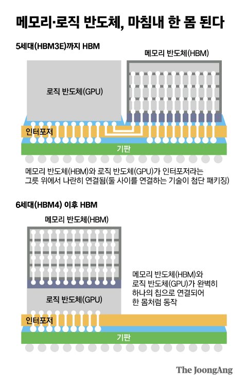
SK Hynix has started recruiting design personnel for logic semiconductors such as CPUs and GPUs, reports Joongang.co.kr. The company is apparently looking to stack HBM4 directly on processors, which will not only change the way logic and memory devices are typically interconnected but will also change the way they are made. In fact, if SK Hynix succeeds, this may transform the foundry industry.
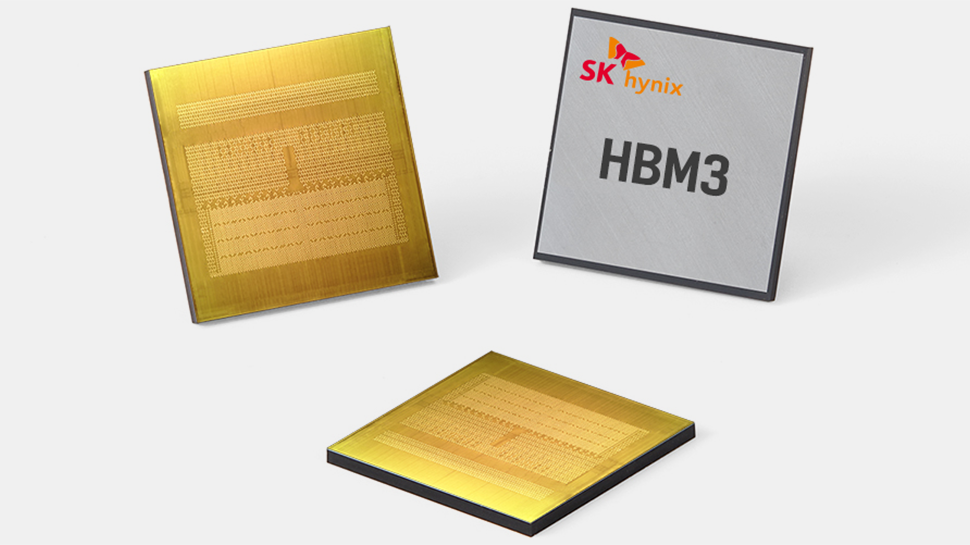
Nowadays HBM stacks integrate 8, 12, or 16 memory devices as well as a logic layer that acts like a hub. HBM stacks are placed on the interposer next to CPUs or GPUs and are connected to their processors using a 1,024-bit interface. SK Hynix aims to put HBM4 stacks directly on processors, eliminating interposers altogether. To some degree, this approach resembles AMD's 3D V-Cache, which is placed directly on CPU dies. But HBM will feature considerably higher capacities and will be cheaper (albeit slower).
SK Hynix is reportedly discussing its HBM4 integration design method with several fabless companies, including Nvidia. It's likely that the two companies will jointly design the chip from the beginning and produce it at TSMC, who will also put SK Hynix's HBM4 device on logic chips using a wafer-bonding technology. A joint design is inevitable in order for memory and logic semiconductors to work as one body on the same die.
The HBM4 memory will use a 2,048-bit interface to connect to host processors, so interposers for HBM4 will be extremely complex and expensive. This makes the direct connection of memory and logic economically feasible. But while placing HBM4 stacks directly on logic chips will somewhat simplify chip designs and cut costs, this presents another challenge: thermals.
Modern logic processors, such as Nvidia's H100, consume hundreds of watts of power and dissipate hundreds of watts of thermal energy. HBM memory is also rather power-hungry. So cooling down a package containing both logic and memory could require very sophisticated methods, including liquid cooling and/or submersion.
"If the heating problem is solved two to three generations later than now, HBM and GPU will be able to operate like one body without an interposer," said Kim Jung-ho, a professor in the Department of Electrical and Electronics at KAIST.
But the integration of memory directly on processors will also change how chips are designed and made. Producing DRAM using the same process technology as logic and on the same fab will guarantee ultimate performance, but will increase memory costs dramatically, so this is not an option that is seriously considered right now. Nonetheless, it looks like memory and logic are poised to get closer, both literally and on the process technology level.
Get Tom's Hardware's best news and in-depth reviews, straight to your inbox.
"Within 10 years, the 'rules of the game' for semiconductors may change, and the distinction between memory and logic semiconductors may become insignificant," an industry insider told Joongang.co.kr.

Anton Shilov is a contributing writer at Tom’s Hardware. Over the past couple of decades, he has covered everything from CPUs and GPUs to supercomputers and from modern process technologies and latest fab tools to high-tech industry trends.
-
hotaru251 tbh anything that pushes advancement (and hopefully drip down to consumer) of submersion cooling is all good in my book :|Reply
its literally the one tech thats been mentioned for decade but hasnt really advanced to market. -
bit_user I see this as the logical follow-on from prior HBM PIM (Proccessing In Memory) efforts.Reply
https://www.tomshardware.com/news/samsung-hbm2-hbm-pim-memory-tflops
SK Hynix announced a version, also. I'm too lazy to look it up.
AMD also seems headed in this direction, as it's in line with their Zettascale roadmap.
"Within 10 years, the 'rules of the game' for semiconductors may change, and the distinction between memory and logic semiconductors may become insignificant," an industry insider told Joongang.co.kr.
I'm not too sure about that. HBM isn't scaling to higher capacities like DIMMs can. I think there will always be a need for some plain, old DRAM that lacks any integrated computation. It could be a slower tier, connected via CXL, that sits in between the HBM tier and the SSD tier. -
alan.campbell99 Hmm. We're already seeing a rise in power draw, enough to bring water-cooled servers into consideration. Perhaps this sort of thing will accelerate that? I'd hope there's some efforts ongoing to deal with this rather than just keep on increasing the power draw of processors. I think it was around the Pentium MMX time that someone I worked with would respond to customers that their PC would use a similar amount of power to an incandescent light bulb.Reply -
bit_user Reply
Yuck. Submersion cooling is messy and expensive. I'm not interested.hotaru251 said:tbh anything that pushes advancement (and hopefully drip down to consumer) of submersion cooling is all good in my book :|
I think it's continuing to make inroads into HPC and some datacenters. That's where it should stay, IMO.hotaru251 said:its literally the one tech thats been mentioned for decade but hasnt really advanced to market. -
bit_user Reply
AMD's Fury was the first GPU to use HBM, but it worked by placing the stacks next to the compute die. This is fusing the HBM atop the compute die. That's the key difference.ingtar33 said:wasn't this what vega was about? -
bit_user Reply
That's not germane to the issues discussed in the article. They're concerned about how to get heat from the die to the exterior of the package (or, I guess the top of the stack, if you're doing direct-die cooling).alan.campbell99 said:Hmm. We're already seeing a rise in power draw, enough to bring water-cooled servers into consideration. Perhaps this sort of thing will accelerate that?
According to this, no Pentium MMX version used more than 17 W.alan.campbell99 said:I think it was around the Pentium MMX time that someone I worked with would respond to customers that their PC would use a similar amount of power to an incandescent light bulb.
https://en.wikipedia.org/wiki/Pentium_(original)#Models_and_variants
I remember seeing the inside of a Compaq desktop, with a Pentium MMX, and the thing still had a passive heatsink! It was big and aluminum, but definitely had no integrated fan.
Nothing else inside that PC should've used very much power. Graphics cards of the day had tiny fans, if any, and HDDs rarely burn more than 10 W. That would put even 60 W (which is pretty low, for a conventional screw-in, incandescent lightbulb) as an overestimate. -
thestryker This seems like something untenable for consumer space due to the clockspeeds desktop silicon typically runs at to make up for smaller chips. No matter what you'd probably need backside power delivery to make this work period as HBM stacks aren't exactly lacking in z-height. It would take an absolute revelation in manufacturing to make memory and logic on the same process so this is extremely unlikely. It makes sense that they're talking about HBM 4 since that's 2026+.Reply -
TechLurker On the cooling front, I'm reminded of a recent news article where a breakthrough was made in integrating some kind of cooling directly into the dies, allowing for transferring the heat out to say, a copper sideplate that a cooler could contact alongside the die itself, allowing for a wider cooling surface even as dies shrink.Reply
I wonder if that will be implemented along side this. -
williamcll They are taking the apple approach where if your memory dies you have to replace the entire processor.Reply
