Return To Castle Intel: 16 Years Of Motherboard History
Get Tom's Hardware's best news and in-depth reviews, straight to your inbox.
You are now subscribed
Your newsletter sign-up was successful
Return To Castle Intel
Last month, we took you deep into the hidden recesses of Intel’s Hawthorn Farm facility, where the company’s enthusiast motherboards are designed and refined. On our way out of the building, we walked down a long hallway that ends with the metal detector gate one passes through when entering the building. This hallway is lined with dozens of mounted, framed motherboards—a veritable walk-through museum documenting Intel’s many years of motherboard innovation.
As tech enthusiasts, we tend to be amnesiacs. There’s just so much good stuff to focus on now, and even better stuff coming soon, that we forget where we’ve been and the massive effort that went into moving through those stages. Walking this hallway, we felt a bit like archeologists or perhaps sudden visitors to the Galapagos Islands, granted a rare glimpse at the sweep of natural evolution. Some fits of creativity grew into the technologies we have today. Others blossomed for a moment and died ingloriously.
At the end of our last visit, we got about half-way down this hallway, then stalled in our tracks. After nearly two decades in the hardware business, it was impossible not to stop at each frame with a “I remember that!” or a “Oh, what was that called again?!” We wanted to stay for hours. So on a return visit with a camera and tripod, we did. Sure, we had to shoot the boards under poor lighting and through the high-glare glass of their frames, but it turned out well in the end.
What follows are our picks for the best dozen of the mobo brood, the ones that stood out as having exceptional historical significance. We had a blast taking this walk down memory lane and rediscovering our roots. Hopefully, you will, too.
I’m Batman
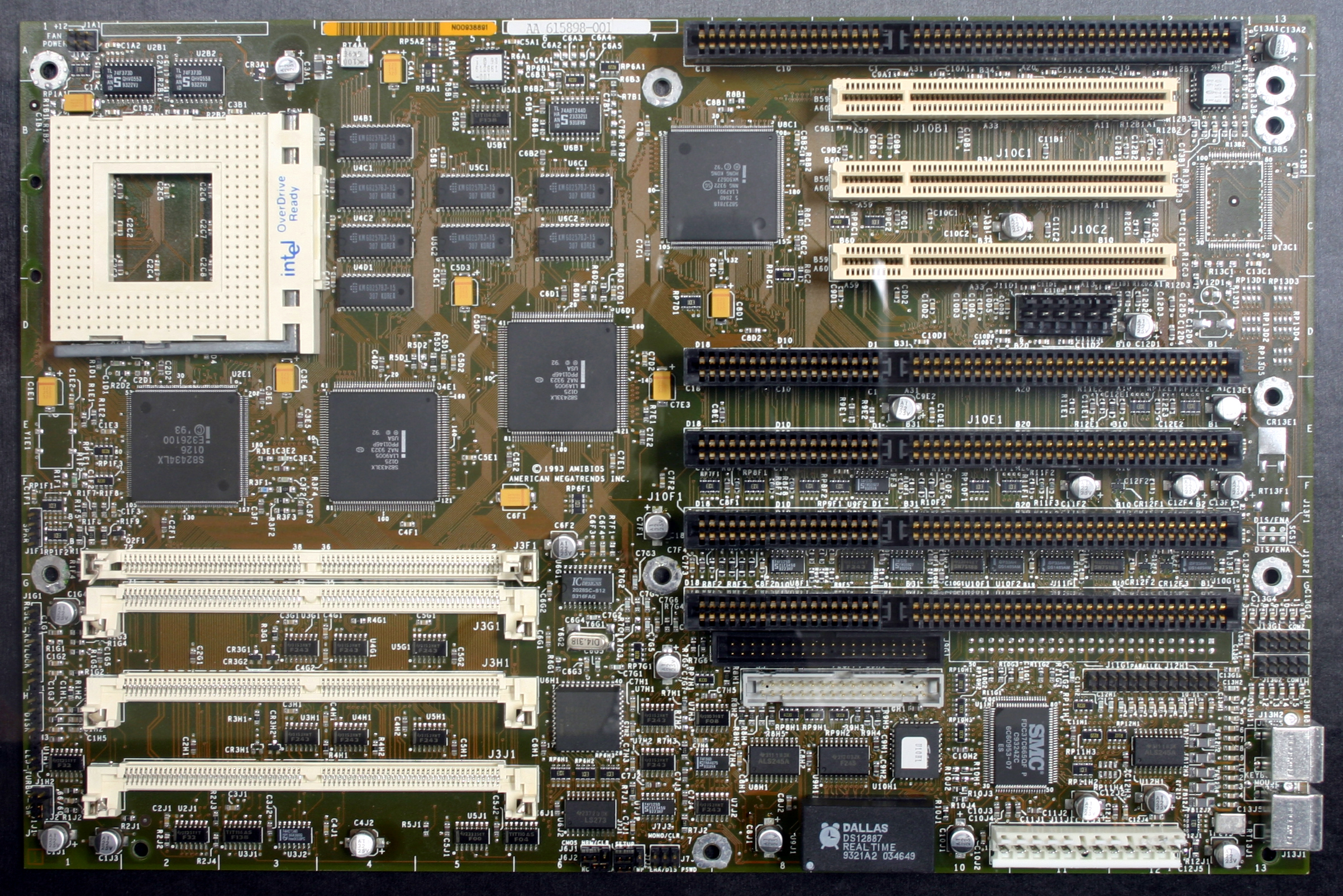
For you trivia buffs, the original Batman TV series debuted in 1966. Twenty-seven years later, Intel delivered the “Batman” motherboard, the first commercial release from the company’s motherboard group. Prior to Batman, Intel had merely produced reference boards for major OEMs and MNCs (multi-national corporations). The trouble was that the CPU group would launch a chip but there were no motherboards on the market to support it. Intel was stuck in a chicken-and-egg conundrum, and the best solution was to release both items together. Marketing-speak for this is “time to market,” or TTM. Batman was Intel’s first TTM board, and it was meant to accelerate the adoption of Pentium.
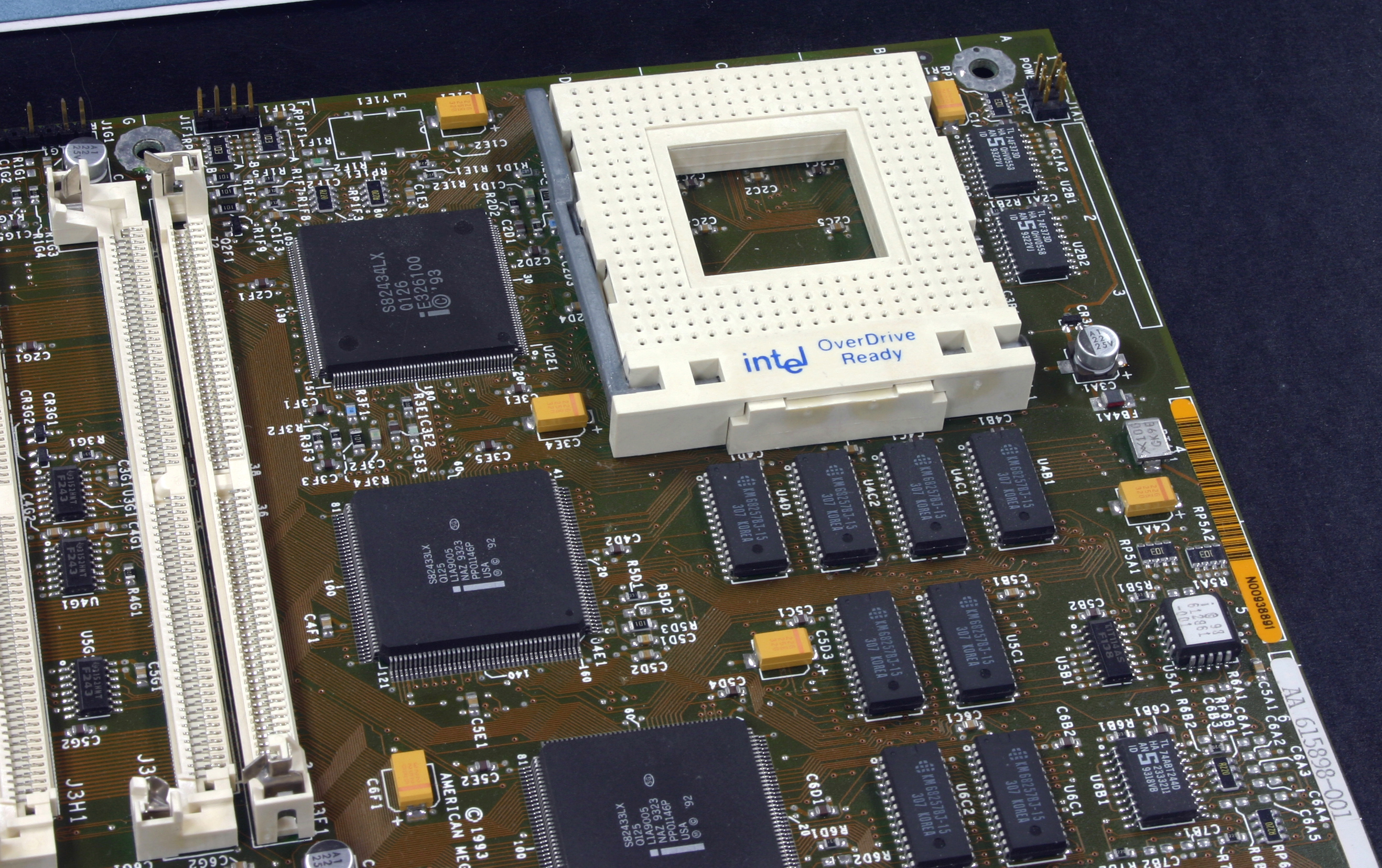
Those rectangular chips near the CPU socket are cache, because L2 had yet to be integrated into the processor. And the big, square chips? No, those aren’t part of the chipset. They’re for I/O.
Less Is...Less
One thing you’ll notice on the really old boards is that some of the SIMM slots closer to the board edge are angled 45 degrees. This was due to chassis height restrictions for items like the hard drive or power supply. The real nugget here is the “OverDrive Ready” stamp on the CPU socket (Socket 4), a feature so ancient that it stumped our first set of Intel engineers. Socket 4 supported a 5V connection and only worked with the Pentium 60 and 66 chips. Socket 5 (3.3V) would later support the Pentium 75 to 133 and used staggered pin rows. The Pentium OverDrive chip used a clock doubler to take the speed to 120 or 133 MHz on Socket 4 systems. The net result was slower than a true 120 or 133 MHz product, but it was the poor man’s answer to a system upgrade. There were also OverDrive chips for Socket 5, Pentium Pro, and, most famously, the 486, which allowed a Pentium core to run on a 486 platform with somewhat hit and miss results.
Get Tom's Hardware's best news and in-depth reviews, straight to your inbox.
Not Much I/O, Is There?
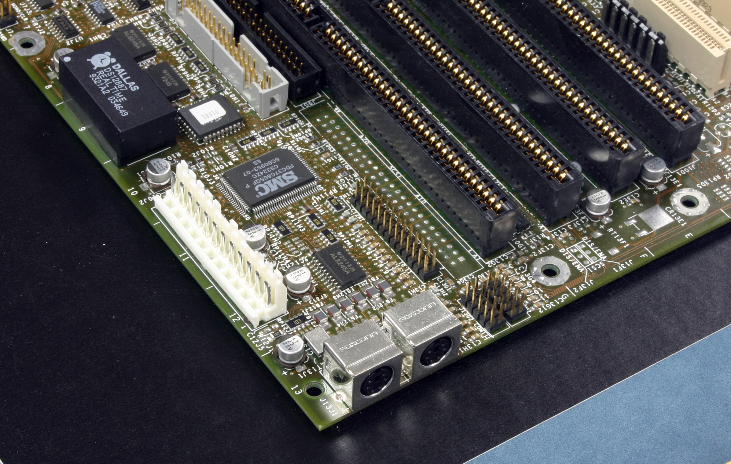
In 1993, Bill Clinton became President, CERN unleashed the World Wide Web, and motherboards integrated practically nothing. That’s right—the only I/O integrated on Batman is a couple of PS/2 ports. If you wanted to add audio, you could use one of those ISA buses for something like a Sound Blaster Pro. That monster-sized Dallas DS1887 real-time clock could select between Motorola and Intel bus timing. (Motorola timing? Chalk that one up to the round file of history.)
Plato Power
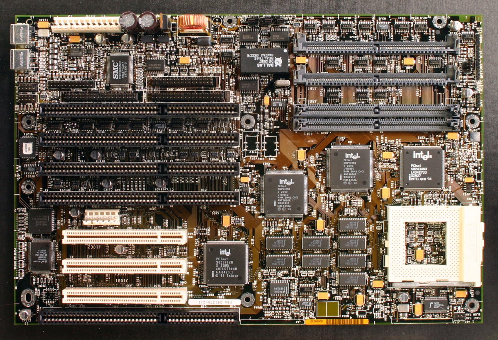
By September of 1994, Intel was ready to bail on the 5V Pentium plan. The Plato motherboard jumped to Socket 5 while preserving many of Batman’s quirks. You still only find PS/2 on the back. There’s 256KB of cache mounted on the PCB—a laughable amount compared to the several megabytes now baked into modern CPUs—and the board could support system memory configurations up to 128 MB across two banks. Plato supported Pentium 75 or 90 chips, and there was a jumper on the motherboard (JP7) you had to set in order to enable the correct processor.
Gateway came out with an OEM version of Plato called Neptune, which just makes you wonder if someone in the company erroneously thought the name was Pluto and wanted to be one planet closer to Earth.
Lotsa Slots
The Plato motherboard was famous within Intel for being the first model to sell over one million units for the company. It was also a sign of the times that boards should be loaded with as many slots as possible—five ISA and three PCI in this case. Maximum expansion capability, summed up by the phrase “slots and watts,” was both a sign of coolness as well as a practical necessity since practically nothing was built into the board. Not how close together the last PCI slot is to the ISA slot on the board’s edge. This was one of the first instances of a shared slot design, in which either slot could make use of one opening in the chassis’s rear.
Other curiosities: Notice how there are no plastic walls around the floppy and hard disk headers on Plato, although there were on Batman? This is an odd step backward since it was all too easy to bend pins during cable attachment and removal. Enough bending and you’d snap a pin or two clean off. And do you see that power connector between the fourth ISA and first PCI slots? Not even the oldest of the Intel old timers helping us could remember what that was for. Bonus kudos to anyone who can solve the mystery in our feedback section.
Thor Strikes
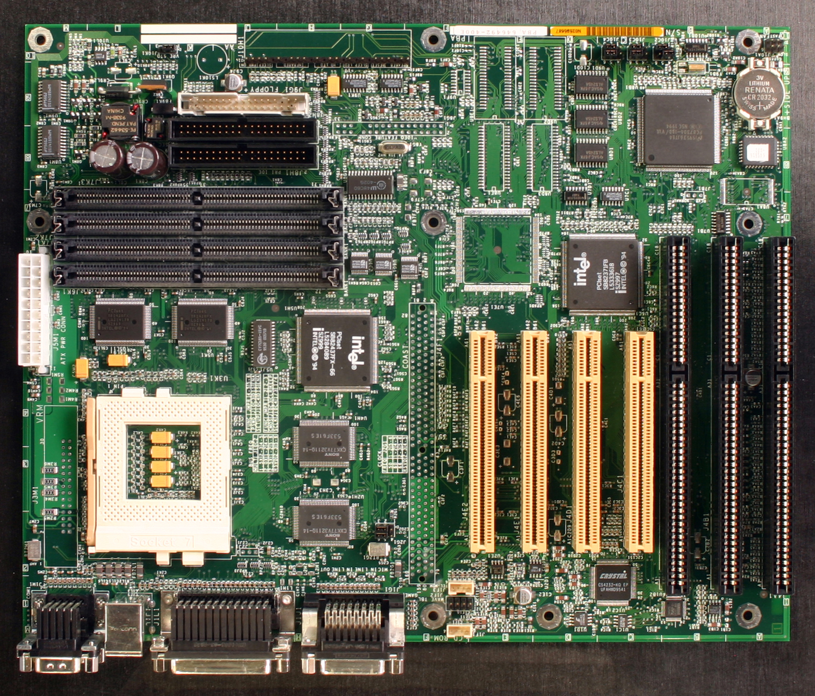
By the beginning of 1996, the industry was in clear need of a return to the simple form factors that made AT and Baby AT desktops so easy to work with, only without AT’s legacy technologies. Intel had released the first specification for ATX in 1995, and Thor was the first Intel board to use the new form factor. While ATX has been updated a few times, the form factor, along with its microATX derivative, still remains the dominant format used in PCs today.
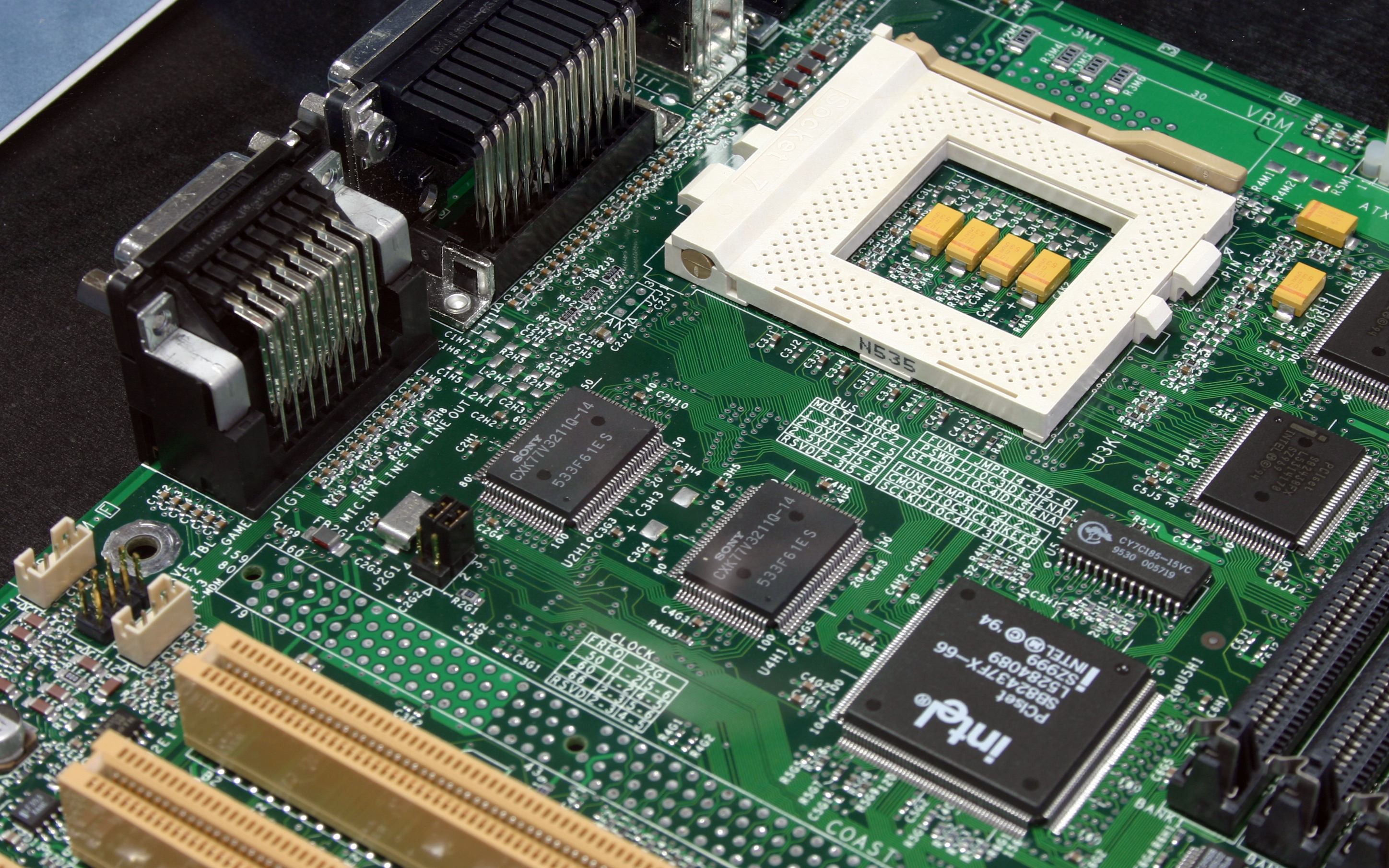
Thor featured a maximum bus speed of 66 MHz for Socket 7 Pentiums and up to 128MB of Extended Data-Out (EDO) SIMM memory. EDO marked a 10% to 15% improvement over the prior Fast Page Memory technology by allowing the memory controller to start a new column address instruction while concurrently reading a different address—multitasking. Of course, this required support in the chipset, and Thor’s Triton (430FX) core logic proved to be immensely popular and really established Intel as a leading chipset company. Triton also supported PCI level 2.0 and pipelined burst cache.
You’ll notice several blank spots on this Thor model. That’s because it was common for Intel, then as now, to produce reference designs that OEMs could then customize to taste. Not everyone needed an extra ISA slot or additional on-board memory.
An Open Intel Platform?
There are a lot of nifty tidbits on this board. The Socket 7 design was novel, not only because it provided split rail voltage—what? over 10 years before AMD made a fuss about Barcelona’s split rail power?—but it was also backward compatible with Socket 5 CPUs. Imagine that, a backward compatible CPU socket. Better yet, Socket 7 worked with processors from AMD, Cyrix, IDT, and others. True, friendly, open craziness. No wonder it didn’t last. And hey, believe it or not, those are Sony 32-bit SRAM chips sitting alongside the CPU socket.
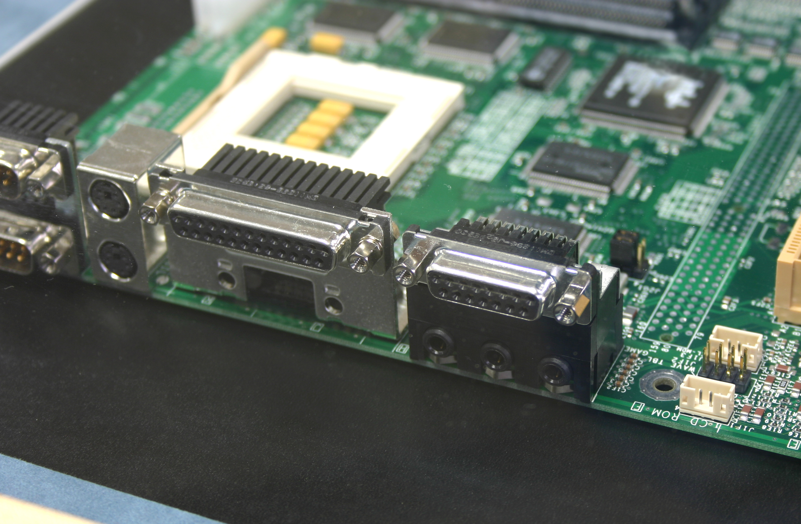
Let The Integration Begin
Looking behind the board, it’s a little miracle--the birth of motherboard integration. Forget those Super I/O cards. Now we have integrated serial, parallel, and game ports. Remember 15-pin game ports for joysticks (support for these disappeared under Windows Vista)? Under the game port, behold—three audio jacks fueled by a Crystal Semiconductor ASIC mounted under the third and fourth PCI slots. In the bottom-right of the image below, you can also see the four-wire audio header for connecting to the CD-ROM so systems could play music discs.
Welcome To Seattle
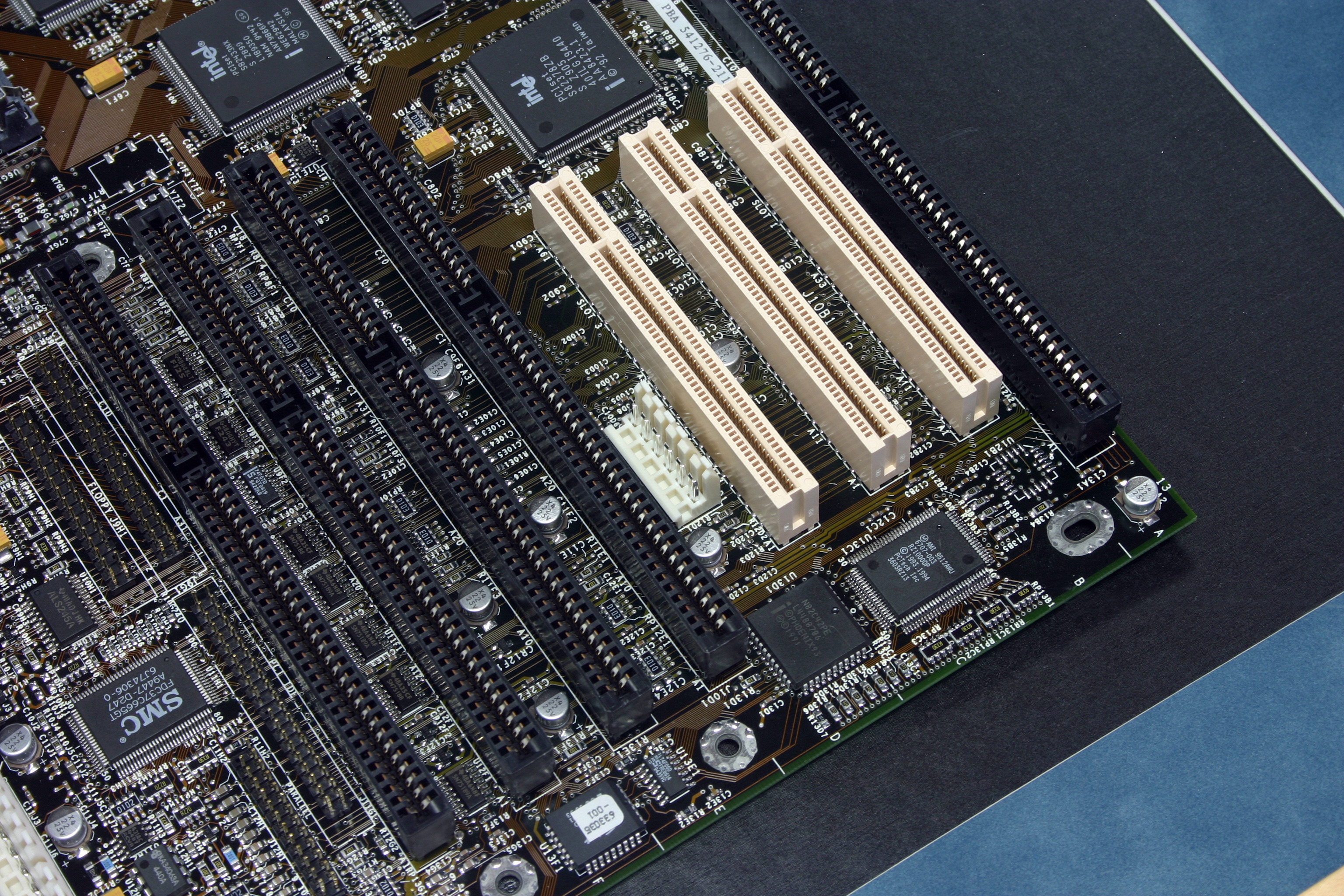
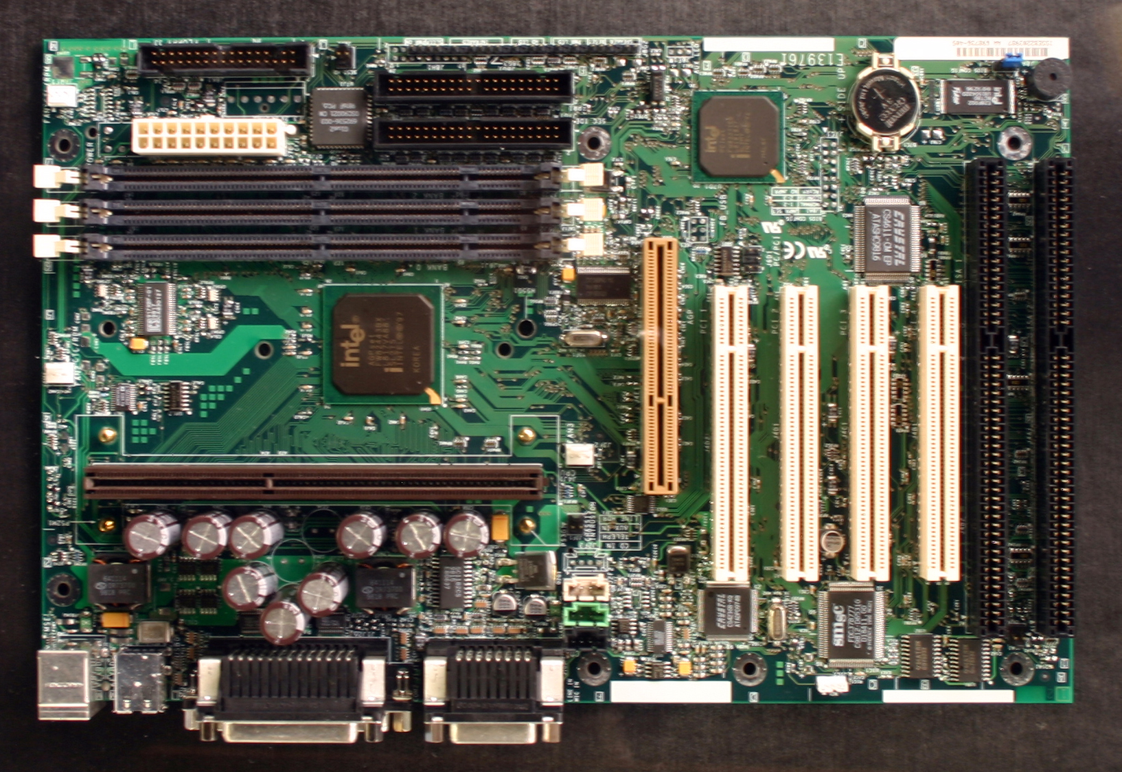
You’d think that our first Intel board code-named for a place might have been Santa Clara, Hillsboro, Portland, or some other major Intel location. But no. The first quarter of 1998 brought us Seattle, Intel’s first board to make it to a 100 MHz front-side bus (FSB). This was also the company’s time-to-market board for supporting the Pentium II launch. Hmmm, where is that CPU socket? Oh, right—there wasn’t one! Instead, we had the Slot 1 design supporting processor cartridge packages often informally known as “candy bars.” Launch speeds of the 100 MHz bus parts were 350 and 400 MHz.
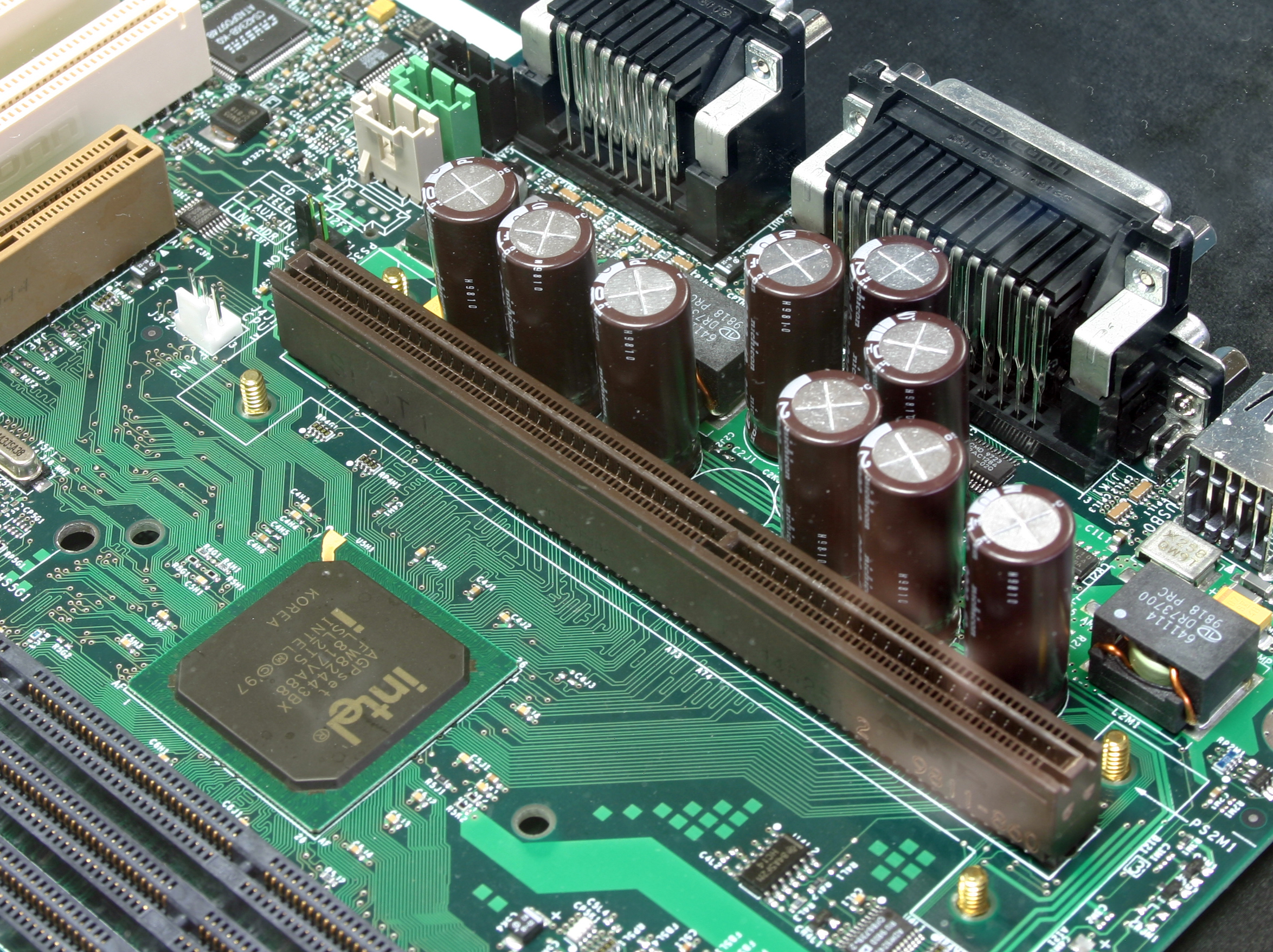
Compared with Thor, you can see that Seattle is a cleaner board. A lot of the extra and oversized chips are vanishing. All of those real estate-sucking memory chips are gone, for instance, although 512KB of L2 cache is still on the motherboard, and large capacitors are starting to crop up like mushrooms around the CPU slot. Note again that we have a shared PCI/ISA slot, this time second in from the far edge.
AGP Redux
Integration takes another hop on Seattle, this time in the form of a pair of USB ports, so new at this time that hardly any devices were available to use them. The USB functionality derived from the PIIX4E southbridge controller. Even more significant was the 440BX northbridge, which was the second from Intel to support Accelerated Graphics Port (AGP). The AGP slot is peeking out to the left of the Slot 1 interface.
-
ravenware Nice article. My only critique would be ending it with the skulltrail platform. It wasn't a breakthrough, both in terms of performance and innovation. AMD produced a similar system a year before Skulltrail in hopes of regaining its performance crown by pulling out the big guns, unfortunately that beast couldn't outperform Intel's quad core chip.Reply
The Skulltrail had similar results, offering very little performance gains over single socket systems while costing and arm and a leg to build and run.
http://www.tomshardware.com/reviews/intel-skulltrail-part-3,1770-25.html
http://www.tomshardware.com/reviews/brute-force-quad-cores,1371-13.html
-
old time jon I am not even finish reading but have fond to many errors that I will stopReply
EX:
-AGP came from the LX chipset not the BX
-PII starting clock where 233Mhz and 266Mhz
-FX chipset had not cache on the board it was on the slot with the CPU
actually the 233Mhz had a really strange cache mem divider that gave it really slow cache access compared to the 266Mhz variant if memory serv well? -
old time jon also could you please give us back the drop down menu for changing back to the right article page?Reply -
swyn01 The unknown power connector you mention on the Plato motherboard is an ATX 6-pin auxiliary power connector. It was used if motherboard drain was to exceed 250 watts. With this many slots it must have been possible to exceed this. I still have ancient power supplies lying (as keep sakes) that have this connector. However, I have never found the need to connect it myself.Reply -
cangelini old time jonI am not even finish reading but have fond to many errors that I will stop EX:-AGP came from the LX chipset not the BX-PII starting clock where 233Mhz and 266Mhz-FX chipset had not cache on the board it was on the slot with the CPUactually the 233Mhz had a really strange cache mem divider that gave it really slow cache access compared to the 266Mhz variant if memory serv well?Reply
Jon,
You're right about the chipset--the LX was, in fact, first with AGP.
I believe the author was referring to 100 MHz bus models--clarified that.
I believe you're incorrect about the 430LX, though--it did support onboard pipelined burst cache memory.
As for the drop-down menu, it appears on all reviews. However, you can navigate through picture stories using the little boxes up top, which also give you a preview of each page before you click.
Thanks, and all the best.
Chris -
swyn01 ReplyI believe you're incorrect about the 430LX, though--it did support onboard pipelined burst cache memory.
You're correct that some slot 1 boards did offer onboard pipelined cache. Often it was an add on option with its own socket but some definitely did have soldered in out of the box. -
Shadow703793 Well done! Next, do a history of OCing. AFAIK OCing has existed as long as these boards.Reply -
old time jon swyn01You're correct that some slot 1 boards did offer onboard pipelined cache. Often it was an add on option with its own socket but some definitely did have soldered in out of the box.Reply
I may yet learn something here? Seing as the L2 cache on slot 1 CPUs was on the sloted card itself did this soldered on cache on the motherboard become L3 or was it just deactivated?
-
old time jon swyn01You're correct that some slot 1 boards did offer onboard pipelined cache. Often it was an add on option with its own socket but some definitely did have soldered in out of the box.Reply
I do remember this option on the socket 5-6-7 motherboards. Some super 7 motherboard went a far as 1mb cache with depending on the CPU would be L2 or L3 cache. -
http://www.tomshardware.com/picturestory/498-29-intel-skulltrail-badaxe.htmlReply
isn't the fan for the chipset and not the processor?

