Return To Castle Intel: 16 Years Of Motherboard History
Get Tom's Hardware's best news and in-depth reviews, straight to your inbox.
You are now subscribed
Your newsletter sign-up was successful
More AGP
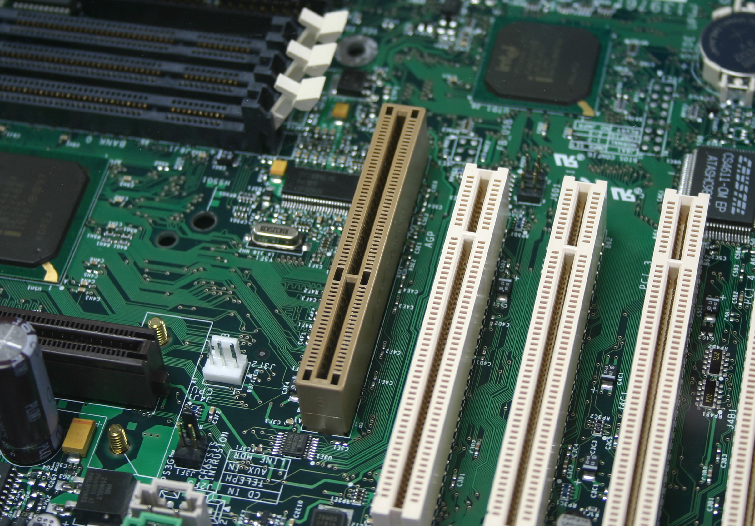
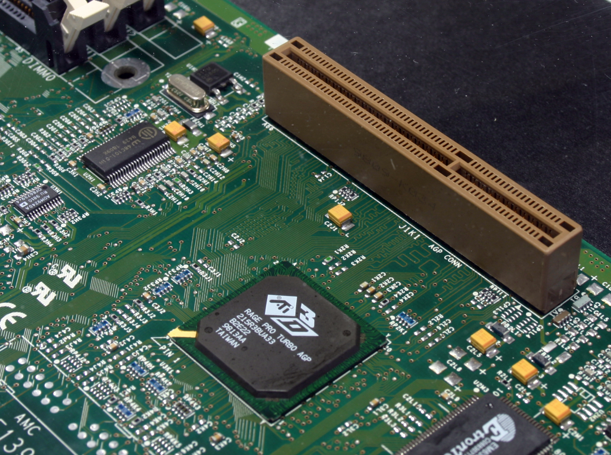
AGP marked a quantum leap beyond graphics utilizing the shared PCI bus. Seattle supported AGP at 66 and 133 MHz speeds. To modern eyes, the idea of debuting a new graphics technology on a business platform seems backwards. Times have changed.
Juneau About NLX?
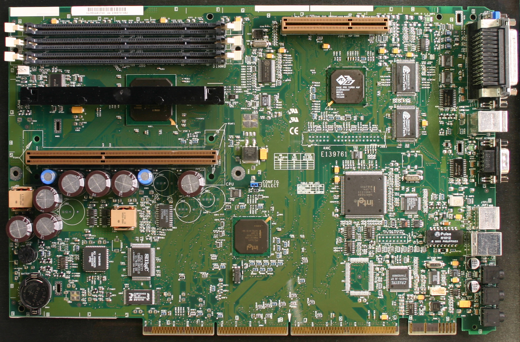
Only one month after Seattle’s arrival, Intel took the 66/100MHz FSB Pentium II in a different direction. The Juneau motherboard is the only product in this roundup to use the NLX form factor. NLX was a bona fide industry standard and perhaps the industry’s first widespread attempt at the small form factor concept. The former LPX design lacked NLX’s component interchangeability. Unlike today’s small form factor standards, though, NLX relied on either a three-slot or four-slot riser card for ISA and PCI slot expansion. The riser plugged into the edge connector along the side of the motherboard, turning the board into an L-shape. This is why you only see two slots on the riser-less Juneau. One was for the Pentium II cartridge (that black bar was a bracket for securing the CPU heatsink), and the other was for AGP 2x cards.
Getting Down To Business
In 1998, slimline systems, the dominant application for small form factor, were primarily a corporate phenomenon. SFF was a long way from taking hold in the consumer world. And because mainstream corporate boxes could be even more price sensitive than consumer desktops, the push for integration was even more paramount. This is why Juneau has integrated 10/100 Ethernet as well as an onboard ATI RAGE Pro Turbo 64-bit AGP chip, a pretty slick feature in those days.
Integration Galore
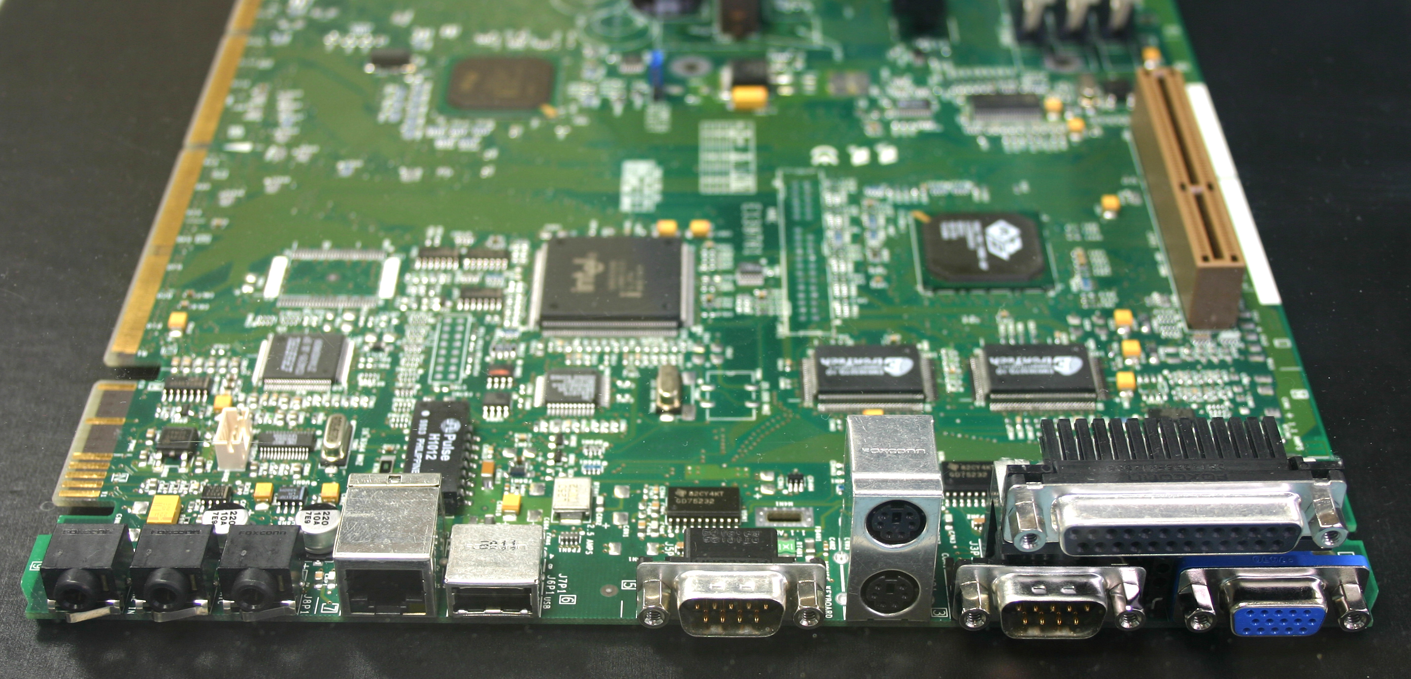
There’s no game port—another business-oriented tell-tale—but VGA, audio (including a front panel audio header), and a single USB port are all splashed across the back edge in seemingly random order.
A Bridge Too Far In Vancouver
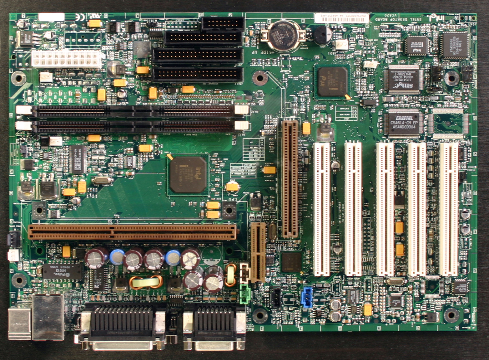
Vancouver is a small city, just outside of Portland, OR, and across the Columbia River in Washington. The commute to Intel’s facilities in Hillsboro from Vancouver was atrocious in 1999 (and hasn’t improved any since). One might even call it overextending. Perhaps this was the psychic backdrop behind the Vancouver motherboard, better known as the VC820, which was Intel’s first board to use Rambus DRAM, or RDRAM. Suffice it to say here that RDRAM may be the single worst black eye Intel ever suffered in its motherboard division.
Intel and Rambus became financially entangled in 1996, and not long thereafter Intel announced that it would standardize on the Rambus memory interface. The move was a bit like announcing in 2009 that all cars need to be electric by 2012, only electric cars cost more, run slower, can’t travel as far, and are way more expensive to repair—oh, and you have to consume as many fossil fuels as with gas cars in order to make the electricity. RDRAM looked spiffy on paper, but the technology underperformed DDR and carried a stiff price premium. It made no sense outside of workstation platforms. AMD couldn’t have asked for a better early Christmas present. The public outcry was intense, and RDRAM died a remarkably premature death.
Get Tom's Hardware's best news and in-depth reviews, straight to your inbox.
Some Good News
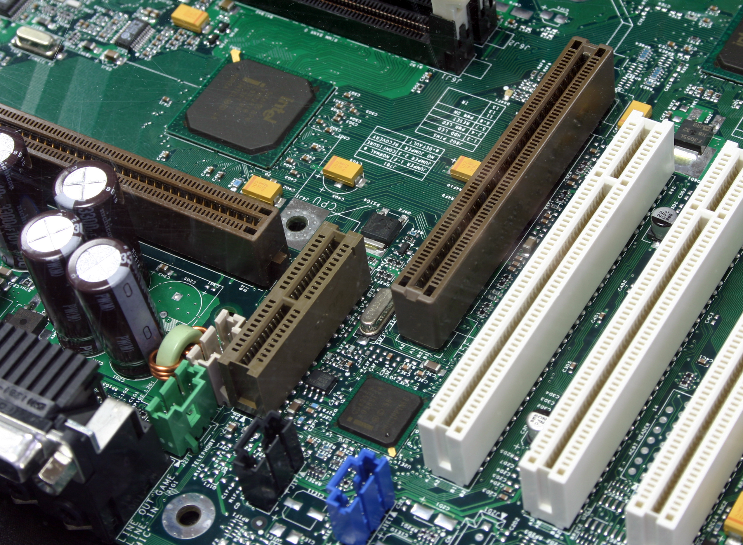
Sorry, we were talking about motherboards. Aside from RDRAM, and the ridiculous need for what were essentially electrical dummy modules called CRIMMs if you only wanted to run a single memory stick, Vancouver wasn’t a bad product. The AGP slot supported up to 4x cards.
More Vancouver
There were four dual-color diagnostic LEDs on the back for diagnostics, a surprising twist that foreshadowed future enthusiast leanings. The motherboard and its 820 chipset could run both Pentium II and Pentium III processors with host bus speeds of 100 or 133 MHz.
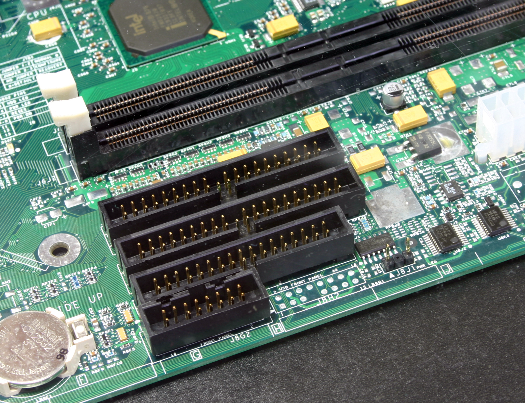
Vancouver also features a new slot called the audio/modem riser, or AMR. This was a slick cost-cutting maneuver by which manufacturers could create one analog card for functions such as modem communication or audio and get that daughter card FCC certified. This way, analog I/O could be updated without the complexity or expense of updating the motherboard and having to run it through the FCC again. The board still features a game port on the back panel. The only bit of design weirdness we see here is in the bracketed front panel I/O header (itself a pretty fresh PC concept) below the floppy and PATA ports. Look closely and you’ll see that the I/O bracket is offset from the disk brackets by a fraction of an inch. This wasn’t a flub. The feature outlines screened on the board show the same thing—an unusual bit of aesthetic oversight for Intel. Another interesting point is the outline screen for the AGP locking tab, which was an option not present on this reference board. The view was that the latch was an additional expense at a time when not everyone cared about securing the graphics card.
Little Willow
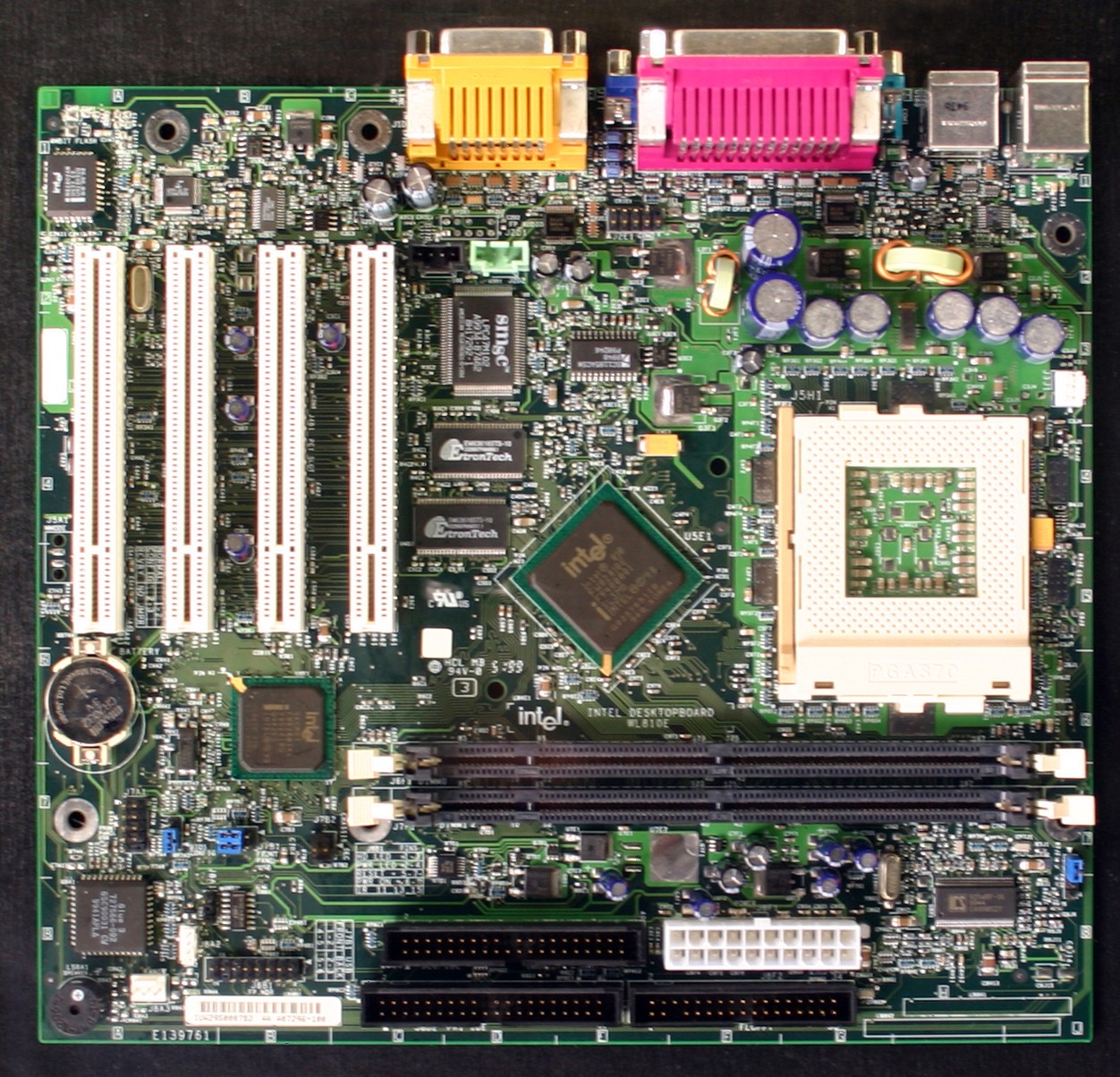
Give Intel credit for fessing up to its mistakes. A year after the RDRAM debacle, we had the Pentium III- and Celeron-based Willow Springs 2, the D810EWS-2, and memory support for up to 512MB of plain ol’ 100 MHz, 168-pin DIMMs. Front-side bus support spanned 100/133 MHz for the P3 and 66 MHz for Celeron. Intel likes to talk about how Willow Springs 2 is significant because it was the company’s first motherboard to be designed in Kulim, Malaysia, at the sister design site to the Hawthorn Farm campus in Oregon. We see it as more significant for its microATX form factor. True, microATX arrived at the end of 1997, well before WS2, but this board was key in popularizing the 9.6" x 9.6" format. It also marked the melting away of the candy bar slot and the return of the socket. Not least of all, Willow Springs 2 marked Intel’s move away from the “superboard” concept. No longer would one board design be adapted for all market segments. Willow Springs 2 was clearly built for the mainstream consumer while Garibaldi (see later) was aimed at the high-end.
One Size Doesn’t Fit All
Apparently, Intel also melted away both ISA and AGP support on this board, leaving only four PCI slots. With no LAN port and a more compact form factor, Willow Springs 2 was making a new play for the consumer market based on integration-driven affordability. One could opt for the inexpensive Celeron, you had on-board Crystal audio, and VGA output from the 810E chipset’s integrated graphics. The newly coined “Graphics Media Controller Hub” featured “vivid 2D and 3D graphics,” “soft DVD MPEG-2 playback,” and “Linux Operating System support.” Woooo. Big stuff back then, even if it did set a multi-year precedent for Intel’s integrated graphics being underwhelming to all but business users.
Check out the introduction of PC 99 color coding on the I/O ports. PC 97, the initial spec of the PC System Design Guide from Microsoft and Intel, mandated that PS/2 mouse ports would be green and PS/2 keyboard ports purple. This was to keep people from plugging the wrong device into the wrong port. PC 99 expanded this with the colors you now see on legacy I/O ports, including blue VGA ports and the multifarious audio jacks.
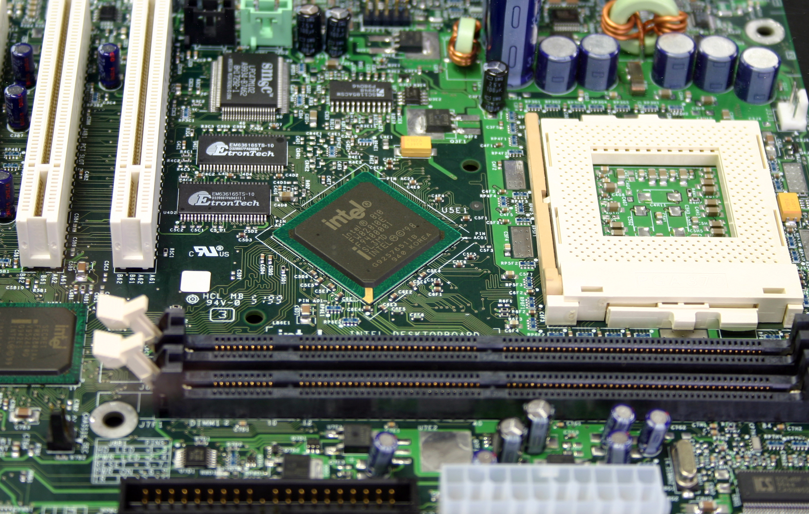
You’re probably wondering about the northbridge being rotated 45 degrees. No, this isn’t some odd harbinger of the defunct BTX form factor—not directly, anyway. There are simply some engineering cases in which the rotation helps simplify and shorten the length of the trace break-outs from the northbridge to the front-side bus, memory, hublink to the southbridge, and expansion slots. Because the mounting holes remain unchanged, there’s no violation of the ATX/microATX form factor.
Enthusiast Roots In Garibaldi
Garibaldi is a tiny town on the Oregon coast most notable for a picturesque grain silo and its proximity to Tillamook, home of the Northwest’s top cheese factory. As far as we can tell, there isn’t the slightest thematic connection with the Garibaldi motherboard (D850GB), Intel’s first recognition of the fledgling gamer market. Maybe one of the engineers has a summer home there.
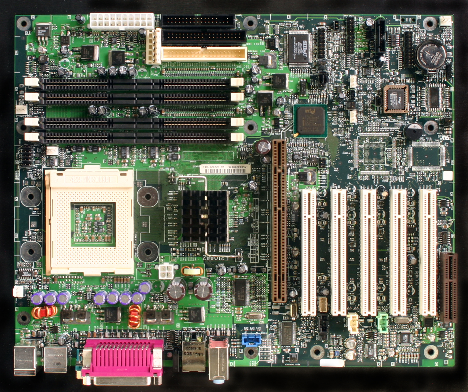
Garibaldi was a full ATX workstation board built for the Pentium 4 with a 400 MHz front-side bus. The high-end slant is evidenced by the presence of a 50W AGP Pro 50 (4x) slot. At the time, Pro 50 cards ran about $1,500 a pop—not so different in concept from stocking your box with 3- or 4-way SLI today. In 2001, this was also one of Intel’s last gasps with RDRAM, and Garibaldi could take up to 2GB of it. You see several signs of mounting power here. Check out the new ATX12V connector by the CPU socket, the auxiliary power connector slammed awkwardly alongside the disk headers, and the northbridge heatsink—the first Intel chipset cooler, near as we can tell.
-
ravenware Nice article. My only critique would be ending it with the skulltrail platform. It wasn't a breakthrough, both in terms of performance and innovation. AMD produced a similar system a year before Skulltrail in hopes of regaining its performance crown by pulling out the big guns, unfortunately that beast couldn't outperform Intel's quad core chip.Reply
The Skulltrail had similar results, offering very little performance gains over single socket systems while costing and arm and a leg to build and run.
http://www.tomshardware.com/reviews/intel-skulltrail-part-3,1770-25.html
http://www.tomshardware.com/reviews/brute-force-quad-cores,1371-13.html
-
old time jon I am not even finish reading but have fond to many errors that I will stopReply
EX:
-AGP came from the LX chipset not the BX
-PII starting clock where 233Mhz and 266Mhz
-FX chipset had not cache on the board it was on the slot with the CPU
actually the 233Mhz had a really strange cache mem divider that gave it really slow cache access compared to the 266Mhz variant if memory serv well? -
old time jon also could you please give us back the drop down menu for changing back to the right article page?Reply -
swyn01 The unknown power connector you mention on the Plato motherboard is an ATX 6-pin auxiliary power connector. It was used if motherboard drain was to exceed 250 watts. With this many slots it must have been possible to exceed this. I still have ancient power supplies lying (as keep sakes) that have this connector. However, I have never found the need to connect it myself.Reply -
cangelini old time jonI am not even finish reading but have fond to many errors that I will stop EX:-AGP came from the LX chipset not the BX-PII starting clock where 233Mhz and 266Mhz-FX chipset had not cache on the board it was on the slot with the CPUactually the 233Mhz had a really strange cache mem divider that gave it really slow cache access compared to the 266Mhz variant if memory serv well?Reply
Jon,
You're right about the chipset--the LX was, in fact, first with AGP.
I believe the author was referring to 100 MHz bus models--clarified that.
I believe you're incorrect about the 430LX, though--it did support onboard pipelined burst cache memory.
As for the drop-down menu, it appears on all reviews. However, you can navigate through picture stories using the little boxes up top, which also give you a preview of each page before you click.
Thanks, and all the best.
Chris -
swyn01 ReplyI believe you're incorrect about the 430LX, though--it did support onboard pipelined burst cache memory.
You're correct that some slot 1 boards did offer onboard pipelined cache. Often it was an add on option with its own socket but some definitely did have soldered in out of the box. -
Shadow703793 Well done! Next, do a history of OCing. AFAIK OCing has existed as long as these boards.Reply -
old time jon swyn01You're correct that some slot 1 boards did offer onboard pipelined cache. Often it was an add on option with its own socket but some definitely did have soldered in out of the box.Reply
I may yet learn something here? Seing as the L2 cache on slot 1 CPUs was on the sloted card itself did this soldered on cache on the motherboard become L3 or was it just deactivated?
-
old time jon swyn01You're correct that some slot 1 boards did offer onboard pipelined cache. Often it was an add on option with its own socket but some definitely did have soldered in out of the box.Reply
I do remember this option on the socket 5-6-7 motherboards. Some super 7 motherboard went a far as 1mb cache with depending on the CPU would be L2 or L3 cache. -
http://www.tomshardware.com/picturestory/498-29-intel-skulltrail-badaxe.htmlReply
isn't the fan for the chipset and not the processor?
