Chipsets Basics
The chipset takes control of all components, which are found on the motherboard. Most sets consist of two chips, which are called North and South Bridge. The North Bridge manages all data transfers between the CPU, main memory and the Accelerated Graphics Port (AGP). Things like I/O-ports (serial, parallel), USB, keyboard controller, AC97 sound, floppy controller and IDE controllers are part of the South Bridge.
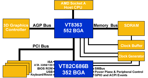
This graphic shows the block diagram of VIA's KT133 chipset for AMD Athlon or Duron processors. Here the North Bridge is called VT8363. VIA's new 686B is pin-compatible with its predecessors, so the one and only difference is the ATA interface.
The North and South Bridge talk to each other via the PCI bus. An exception is Intel's recent chipsets 810, 815, 820 and 840, which come with a different interconnect capable of working at 266 MB/s (twice as fast as the PCI). Also, Intel does not want their chips to be called North and South Bridge anymore, but (G)MCH and ICH (Graphics and Memory Controller Hub, I/O Controller Hub).
