


The X800 Architecture
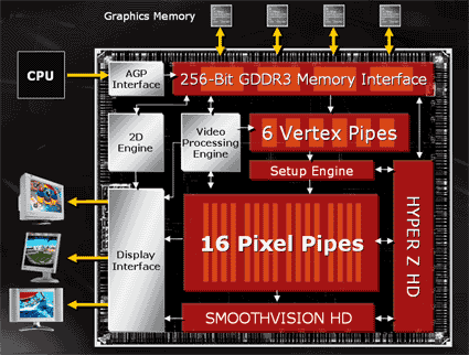
Official R420 block diagram.
The new R420 graphics core shows us how powerful ATi's first DirectX 9 chip R300 really was. While NVIDIA was forced to redesign major aspects of its processor for the changeover from NV30 to NV35/38, and again when switching from NV35/38 to NV40, only a few details of ATi's R300 design have had to be changed since its debut in the Radeon 9700 Pro. Both the Radeon 9800 series and the X800 family presented here are based on this design.
Admittedly, ATi lags behind NVIDIA's 6800 technologically, although it is nearly impossible to tell how great a weakness this will really turn out to be. Until then, the new cards make up for this possible shortcoming by offering excellent performance as well as new goodies such as Temporal FSAA and 3Dc (Normal Map compression).
The X800 Memory Interface
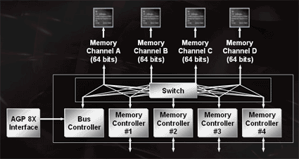
The memory interface of the X800.
The X800's memory interface is 256 Bits wide and subdivided into four channels of 64 Bits. Each channel can simultaneously read and write data to and from memory. A sequencer logic ensures optimal use of the available resources.
Vertex Shader Units
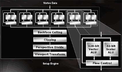
The configuration of the vertex shader units.
ATi has increased the number of vertex shader units from four in the Radeon 9800XT to six in the X800. Together with the higher core clockspeed, this improves the polygon throughput of the new chip quite dramatically. Feature-wise, however, the X800 offers nothing new. Like its predecessors, it too supports VertexShader 2.0