Radeon HD 4850 Vs. GeForce GTS 250: Non-Reference Battle
The Gigabyte GV-N250ZL-1GI: ZL Stands For Zalman
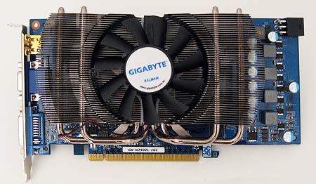
Unlike the somewhat marketing-driven name Matrix, Zalman needs no introduction for most of our readers. For those of you who aren’t in the know, Zalman is a renowned company in the business of making excellent, quiet heatsinks and coolers, among other things. So right out of the gate, just by looking at the massive cooler on the GV-N250ZL-1GI, a person could get the impression that this card is all about cooling. However, there is more here than meets the eye, as Gigabyte has further differentiated this non-reference card by applying its proprietary Ultra Durable VGA feature.
Ultra Durable VGA is the graphics card counterpart to Gigabyte’s Ultra Durable 3 feature set on on some of Gigabyte’s motherboards. We’ve covered the motherboard implementation and performance in this piece.
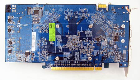
To make a long story short, Ultra Durable VGA is a marketing name for a very similar list of extras: 2 oz. of copper on the PCB, tier-one Samsung or Hynix memory, Japan-made solid capacitors, ferrite core chokes, and low RDS (on) MOSFETs. The tangible benefits that Gigabyte claims Ultra Durable VGA offers is a 5% to 10% lower GPU temperature, a 10% to 30% increase in overclocking ability, and a 10% to 30% reduction in power-switching loss. We’re very interested to see if any of these claims will materialize when we overclock the GV-N250ZL-1GI.
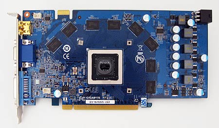
Gigabyte also chose to redesign its PCB instead of just adding the Ultra Durable VGA features to Nvidia’s reference design.
The card is small for a GeForce GTS 250, with the PCB just under 8.5" (about an inch less than the Asus EAH4850 MT). Like its Radeon counterpart, Gigabyte’s GeForce GTS 250 requires a single six-pin PCIe power cable. Gigabyte chose to max out the card’s performance potential with a full gigabyte of RAM, which may impact game performance in titles that rely heavily on the frame buffer. On the downside, Gigabyte chose to only include a single SLI connector on the top of the card, eliminating the possibility of running three GV-N250ZL-1GI cards in 3-way SLI. While this is a theoretical feature loss compared to Nvidia’s reference card, I’m not sure how many folks would realistically want to run three of these cards in tandem, as there are better options out there for that kind of budget.
The default clock speeds for the Gigabyte GV-N250ZL-1GI are 738 MHz on the GPU, 1,836 MHz on the shaders, and 2,200 MHz on the memory. Once again, these are exactly the same as the reference GeForce GTS 250 speeds.
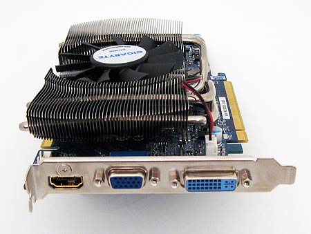
The card has somewhat unique outputs, as Gigabyte has chosen to place an HDMI output, a VGA output, and a single dual-link DVI output on the card. Like the Asus card without two dual-link DVI outputs, the GV-N250ZL-1GI can’t handle two 30” 2650 x 1600 monitors at the same time, but I'm going to go out on a limb and say that a person with two 30" monitors can probably afford a much higher-end card than this. As usual, only two of the three video outputs can be used at any one time.
Get Tom's Hardware's best news and in-depth reviews, straight to your inbox.
Current page: The Gigabyte GV-N250ZL-1GI: ZL Stands For Zalman
Prev Page The Asus EAH4850 MT: Software Next Page The Gigabyte GV-N250ZL-1GI: Software And CoolingDon Woligroski was a former senior hardware editor for Tom's Hardware. He has covered a wide range of PC hardware topics, including CPUs, GPUs, system building, and emerging technologies.
-
tuannguyen rags_20In the second picture of the 4850, the card can be seen bent due to the weight.Reply
Hi rags_20 -
Actually, the appearance of the card in that picture is caused by barrel or pincushion distortion of the lens used to take the photo. The card itself isn't bent.
/ Tuan -
jebusv20 demonhorde665... try not to triple post.Reply
looks bad... and eratic. and makes the forums/coments system
more clutered than need be.
ps. your not running the same bench markes as Toms so your not really comparable.
yes, same game and engine, but for example in crysis, the frame rates are completely different from the start, through to the snowey bit at the end.
pps. are you comparing your card to there card at the same resolution? -
alexcuria Hi,Reply
I've been looking for a comparison like this for several weeks. Thank you although it didn't help me too much in my decision. I also missed some comments regarding the Physix, Cuda, DirectX 10 or 10.1 and Havok discussion.
I would be very happy to read a review for the Gainward HD4850 Golden Sample "Goes Like Hell" with the faster GDDR5 memory. If it then CLEARLY takes the lead over the GTS 250 and gets even closer to the HD4870 then my decision will be easy. Less heat, less consumption and almost same performance than a stock 4870. Enough for me.
btw. Resolutions I'm most interested in: 1440x900 and 1650x1080 for 20" monitor.
Thank you -
spanner_razor Under the test setup section the cpu is listed as core 2 duo q6600, should it not be listed as a quad? Feel free to delete this comment if it is wrong or when you fix the erratum.Reply -
KyleSTL Why a Q6600/750i setup? That is certainly less than ideal. A Q9550/P45 or 920/X58 would have been a better choice in my opinion (and may have exhibited a greater difference between the cards).Reply -
B-Unit zipzoomflyhighand no the Q6600 is classified as a C2D. Its two E6600's crammed on one die.Reply
No, its classified as a C2Q. E6600 is classified as C2D. -
KyleSTL ZZFhigh,Reply
Directly from the article on page 11:
Game Benchmarks: Left 4 Dead
Clearly this is not an ideal setup to eliminate the processor from affecting benchmark results of the two cards. Most games are not multithreaded, so the 2.4Ghz clock of the Q6600 will undoubtedly hold back a lot of games since they will not be able to utilize all 4 cores.
Let’s move on to a game where we can crank up the eye candy, even at 1920x1200. At maximum detail, can we see any advantage to either card?
Nothing to see here, though given the results in our original GeForce GTS 250 review, this is likely a result of our Core 2 Quad processor holding back performance.
To all,
Stop triple posting!
-
weakerthans4 ReplyThe default clock speeds for the Gigabyte GV-N250ZL-1GI are 738 MHz on the GPU, 1,836 MHz on the shaders, and 2,200 MHz on the memory. Once again, these are exactly the same as the reference GeForce GTS 250 speeds.
Later in the article you write,or the sake of argument, let’s say most cards can make it to 800 MHz, which is a 62 MHz overclock. So, for Gigabyte’s claim of a 10% overclocking increase, we’ll say that most GV-N250ZL-1GI cards should be able to get to at least 806.2 MHz on the GPU. Hey, let’s round it up to 807 MHz to keep things clean. Did the GV-N250ZL-1GI beat the spread? It sure did. With absolutely no modifications except to raw clock speeds, our sample GV-N250ZL-1GI made it to 815 MHz rock-solid stable. That’s a 20% increase over an "expected" overclock according to our unscientific calculation.
Your math is wrong. A claim of 20% over clock on the GV-N250ZL-1GI would equal 885.6 MHz. 10% of 738MHz = 73.8 MHz. So a 10% overclock would equal 811.8 MHz. 815 MHz is nowhere near 20%. In fact, according to your numbers, the GV-N250ZL-1GI barely lives up to its 10% minimal capability.


