GeForce GTX 295 Performance: Previewed
GeForce GTX 295, Dissected
Initial speculation was that the GeForce GTX 295 would consist of two GT200s in a configuration that’d emulate a pair of GTX 260s. In all actuality, the card boasts a pair of full-strength GT200s with 240 processing cores each and a more GTX 260-like back-end/memory configuration.
The original GT200 was a 1.4 billion transistor behemoth manufactured using TSMC’s 65 nm node. The version of the chip GeForce GTX 295 employs is die-shrunk to 55 nm. As part of the transition, Nvidia’s Jason Paul claims the company has also made silicon timing changes to improve performance per watt, which should manifest themselves in our discussion of power consumption.
Like the GeForce GTX 280, each GPU on the GTX 295 has, as mentioned, 240 SPs and 80 texture address/filtering units. But, like the GTX 260, the same 295’s GPUs include seven ROP/framebuffer partitions to total 28 ROPs and an aggregate 448-bit path to 896 MB of GDDR3. Vital clocks are also in-line with the GeForce GTX 260. The core clock, including texture/ROPs, runs at 576 MHz. The stream processors run at 1,242 MHz. And the memory runs at 999 MHz (1,998 MHz effective). As you can see, each chip is architecturally right between Nvidia’s fastest and second-fastest ASICs.
| Header Cell - Column 0 | GeForce GTX 295 | GeForce GTX 280 | GeForce GTX 260 | GeForce 9800 GX2 | Radeon HD 4870 X2 |
|---|---|---|---|---|---|
| Manufacturing Process | 55nm TSMC | 65nm TSMC | 65nm TSMC | 65nm TSMC | 55nm TSMC |
| SPs | 480 | 240 | 216 | 256 | 1,600 |
| Core Clock | 576 MHz | 602 MHz | 576 MHz | 600 MHz | 750 MHz |
| Shader Clock | 1,242 MHz | 1,296 MHz | 1,242 MHz | 1,500 MHz | 750 MHz |
| Memory Clock | 1,998 MHz Eff. | 2,214 MHz Eff. | 1,998 MHz Eff. | 2,000 MHz Eff. | 3,600 MHz Eff. |
| Frame Buffer | 1,792 MB Tot. | 1 GB | 896 MB | 1 GB Tot. | 2 GB Tot. |
| Memory Bus Width | 448-bit x 2 | 512-bit | 448-bit | 256-bit x 2 | 256-bit x 2 |
| ROPs | 56 Tot. | 32 | 28 | 32 Tot. | 32 Tot. |
| Price | $499 MSP | ~$380 | ~$230 | N/A | ~$500 |
2 GPUs, 1 Car
d
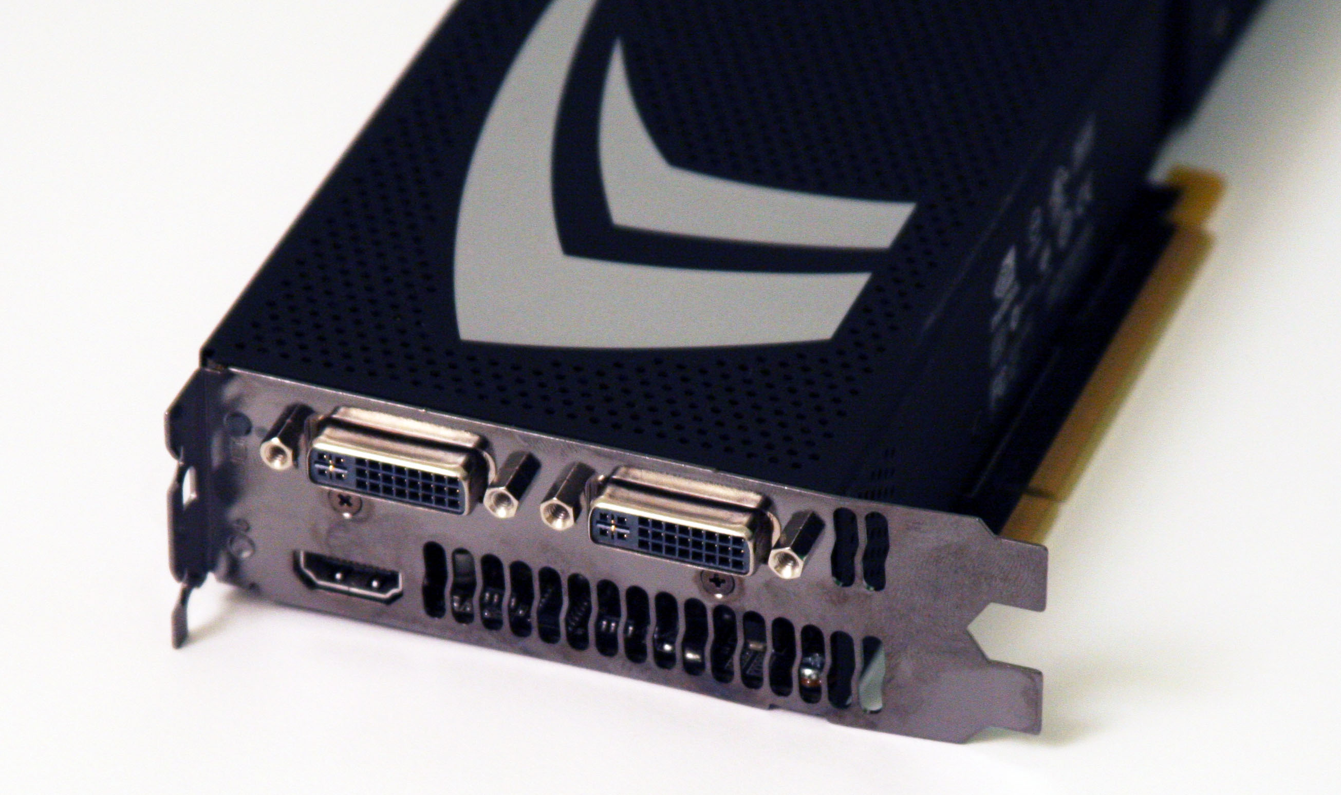
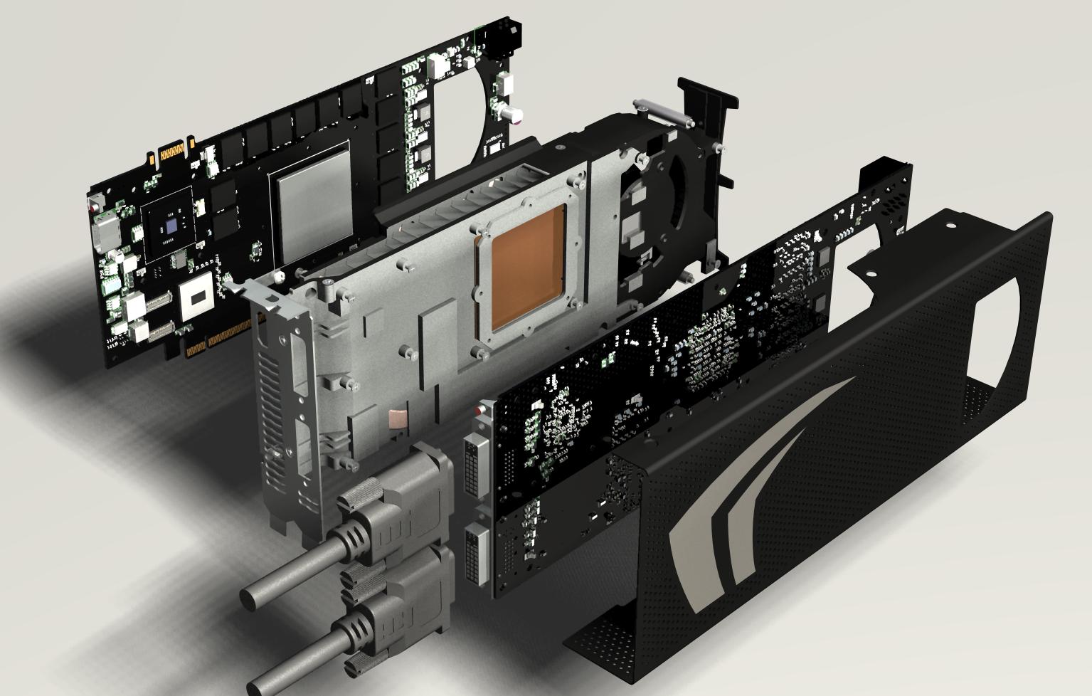
At first glance, the GeForce GTX 295 looks like it could be a 280 or 260. When you flip it onto its stomach and look at the PCB on its back side, it’s clear there is only one GPU there. Like the 9800 GX2 and 7950 GX2 that came before it, this board centers on a dual-PCB design that sandwiches a special heatsink/blower combination between two separate graphics boards linked by an SLI cable and encased in a protective shell.
Naturally, the design of the cooler must be adapted to take the pair of PCBs into account, so you’ll see holes cut in both boards for air to be sucked through. The complete card occupies two expansion slots of space, so it isn’t any wider than Nvidia’s single-chip offerings. In fact, it’s also the same length as the GeForce GTX 280 (and AMD’s Radeon HD 4870 X2).
Let’s Talk Power
Get Tom's Hardware's best news and in-depth reviews, straight to your inbox.
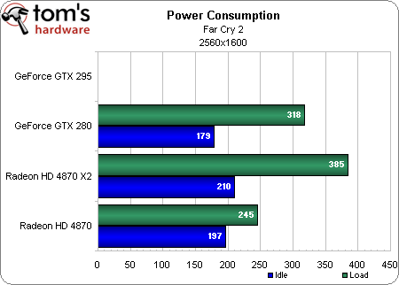
Nvidia isn’t ready to have the GTX 295’s power consumption plotted against AMD’s solution. However, the card as it sits, is less power-hungry at both idle and load than the Radeon HD 4870 X2. The chart below reflects total system consumption from the wall.
On paper, the GeForce GTX 295 uses up to 289 W TDP on its own. The 4870 X2 has a 286 W TDP. And yet, when we measured total system load at the socket, the GTX 295 idled 10 W lower than the AMD board. While looping the Far Cry 2 benchmark at 2560x1600 with AA and AF cranked up, the Nvidia board averaged a full 50 W lower.
Of course, we’ll have to wait until early January for final fan speeds and power figures. But early in the game, the shift to 55 nm is treating the GeForce GTX 295 well, despite the massive size of its GT200 GPU.
Current page: GeForce GTX 295, Dissected
Prev Page Introduction Next Page Test System and Benchmarks-
Tindytim First!?Reply
Why do I get the feeling AMD is already working on something to bust Nvidia again? -
NarwhaleAu Your conclusion was, at best, poor.Reply
Nvidia's "fastest single card" is two 280s on a single PCB, selling at the price point that ATI is selling their 4870x2 at right now?
It is a lot cheaper to produce the 4870 GPU, so I am sure you will see ATI cut their price down by at least $50, and maybe $100. Nvidia will then have the same problem - a monolithic GPU that is expensive to produce and not really any faster than the 4870.
-
xsane I totally agree with him on the Physx and CUDA comment. It would be really nice to have a game like Tiger Woods support Physx.Reply
I have 2 x 4850 in crossfire, it kicks ass. -
trainreks good to see that nvidia whipped back into submission. Their prices were ridiculous when they were on the top for a long time.Reply -
malveaux NarwhaleAU:Reply
You clearly need to re-read this article.
And cutting prices $50? $100? Yea, born yesterday? Not happening.
@Article
Thanks for the preview! I've been looking out for the GTX295 to surface. Two GTX260's should perform right on par with the thing, and I was wondering what the price would turn out to be. You can get GTX260's for $219 from the Egg right now (or $440 for two). If the GTX295 is only a single card at $499 (likely to be 20 less at the Egg), it's right on the same price area as buying two 260's separately. And in that situation, I'd rather have a single card with the same power. As would most folk I wager. So looks like the 295 is gonna be a real winner in the enthusiast market.
Very best, -
JAYDEEJOHN Thanks for being open and honest, and mentioning nVidias mandate. It looks as expected, and is a shame we dont have a larger picture of full performance, since nVidia hamstringed you guys. Good to see some competition at the highendReply -
sparky2010 The problem with ATI is that they release good products but give them incomplete/unoptimized drivers.. to see games where the difference between the 4870 and the X2 is almost nil, but the GTX 295 is doing well in it, well, that's no excuse for ATI.. it's too bad though.. i really hope they could just give us good drivers from the beginning, instead of giving us "performance upgrade packages"..Reply
I hope that their next driver will see more optimization, and then a showdown! CROSSFIRE X vs. QUAD SLI!!!! MUAHAHAHA!
Bets down please?


